Reduced charge recombination in a co-sensitized quantum dot solar cell with two different sizes of CdSe quantum dot
J.
Chen
a,
W.
Lei
*a and
W. Q.
Deng
*b
aSchool of Electronic Science and Engineering, Southeast University, Nanjing, 210096, China. E-mail: lw@seu.edu.cn; Fax: +86-25-83792662; Tel: +86-25-83792650
bState Key Lab of Molecular Reaction Dynamics, Dalian Institute of Chemical Physics, Chinese Academy of Sciences, Dalian, 116023. E-mail: dengwq@dicp.ac.cn; Fax: +86-411 84379571; Tel: +86-411 84379571
First published on 6th December 2010
Abstract
An efficient photoelectrode is fabricated by sequentially assembling 2.5 nm and 3.5 nm CdSe quantum dots (QDs) onto a TiO2 film. As revealed by UV-vis absorption spectroscopy, two sizes of CdSe QD can be effectively adsorbed on the TiO2 film. With a broader light absorption range and better coverage of CdSe QDs on the TiO2 film, a power conversion efficiency of 1.26% has been achieved for the TiO2/CdSe QD (2.5 nm)/CdSe QD (3.5 nm) cell under the illumination of one Sun (AM 1.5G, 100 mW cm−2). Electrochemical impedance spectroscopy shows that the electron lifetime for the device based on TiO2/CdSe QD (2.5 nm)/CdSe QD (3.5 nm) is longer than that for devices based on TiO2/CdSe QD (2.5 nm) and TiO2/CdSe QD (3.5 nm), indicating that the charge recombination at the interface is reduced by sensitizing with two kinds of CdSe QDs.
1. Introduction
Quantum dot sensitized solar cells (QDSSCs) have attracted extensive interest in the past decade as a promising candidate for the third generation of cost-effective photovoltaic solar cell.1 QDs such as CdSe,2 CdS,3 and CdTe4 with their size-dependent band gaps provide new opportunities for harvesting light energy in the visible and infrared regions of solar irradiation.5 QDs are especially appealing for their high extinction coefficients compared to more conventional dyes.6 In addition, through the impact ionization effect, it is possible to utilize hot electrons of QDs to generate multiple electron–hole pairs per photon.7 As a result, the efficiency of this variety of solar cell may exceed the Shockley and Queisser limit (31%).8However, QDSSCs have shown comparatively lower efficiencies than expected. The major challenge of improving the performance of QDSSCs is to inhibit charge recombination at the semiconductor surface. Some strategies have been employed to lower the interface charge recombination. For example, Zhu et al. have fabricated an improved QDSSC with a Zn-doped TiO2 film to reduce the charge recombination.9 The recombination between the TiO2 and electrolyte interface can be significantly reduced by passivation of the photoanode surface with a ZnS coating.10
Herein, we report on the fabrication and characterization of QDSSCs with two different sizes of CdSe QD on a TiO2 film. It was reported that Lee et al. have fabricated a co-sensitized QDSSC by using a solution of two sizes of CdSe QD.11 The improved efficiency was mainly due to the increased photocurrent, which was caused by a co-sensitization effect of the CdSe QDs. In our work, we shall fabricate a co-sensitized QDSSC by loading with the smaller and larger sized CdSe QDs sequentially. The larger sized CdSe QDs coated on the photoanode are used not only as a complementary light absorption layer, but also as a passivation layer to reduce the charge recombination. A power conversion efficiency (PCE) of 1.26% was achieved in this work.
2. Experimental details
Oleic acid (OA)-capped CdSe QDs in toluene solution were synthesized by the one-pot growth method.12 In a three-neck flask, a 70 ml octadecene (ODE) solution containing 5.54 g OA and 0.51 g CdO was firstly heated to 180 °C to form a clear solution under a N2 atmosphere. After that, it was heated up to 230 and 260 °C, respectively, to obtain different sizes of QD. TOP-Se solution (1.3 mmol Se powder and 0.5 g trioctylphosphine dissolved in 10 ml ODE, stirred for more than 1 h) was quickly injected into the flask (within 40 s). The heater was removed 1.5 min later to stop the reaction. Finally, methanol and acetone were added to precipitate the QDs, which were then dissolved in toluene for storage. The OA ligand was exchanged with a mercaptopropionic acid (MPA) ligand for adsorbing the QDs on the TiO2 film. The detailed procedure for the synthesis of MPA-capped CdSe QDs in ethanol solution is described elsewhere.12 MPA-capped CdSe QDs of 2.5 nm and 3.5 nm size are denoted herein as CdSe I and II.TiO2 nanoparticles were fabricated from P25 TiO2 powder (Degussa). 5 g P25 powder was mixed with 180 ml 10 M NaOH and the solution was reacted in an autoclave at 130 °C for 24 h. The product was washed sequentially in 0.1 M HNO3 solution and deionized water, and dried at 110 °C for usage. A TiO2 paste was coated on a fluorine-doped SnO2 (FTO) substrate by the doctor-blading technique. After annealing at 450 °C for 1 h, the TiO2 paste was transformed to a mesoporous film with a thickness of 5 μm and an active area of 0.25 cm2. The bare TiO2 film was directly immersed into the CdSe I and II ethanol solutions sequentially. Meanwhile, the bare TiO2 films were assembled with CdSe I or CdSe II for comparison. The TiO2/CdSe I, TiO2/CdSe II, and TiO2/CdSe I/CdSe II photoelectrodes were assembled with a 20 nm platinum-coated indium tin oxide (ITO) substrate as the counter electrode. The cell gap was maintained by a 60 μm thermal-plastic spacer. The polysulfide electrolyte consisting of 1 M Na2S, 1 M S and 0.1 M NaOH was injected into the cells by the capillary effect. The QDSSCs based on the TiO2/CdSe I, TiO2/CdSe II and TiO2/CdSe I/CdSe II photoelectrodes were denoted cells A, B and C, respectively.
The absorption spectra were recorded using a SHIMADZU MPC-2200 UV-vis spectrometer. The current density–voltage (J–V) characteristics were measured with a Keithley 2440 Sourcemeter and the cell was subjected to the irradiation of a solar simulator (Abet-technologies, USA) operating at 100 mW cm−2 (AM 1.5G). The incident photon to current conversion efficiency (IPCE) was measured with a QE/IPCE Measurement Kit (Oriel, USA) in the wavelength range of 400 to 700 nm. Electrochemical impedance spectra (EIS) were measured under open-circuit voltage with an oscillation voltage amplitude of 10 mV for frequencies from 10−1 to 106 Hz.
3. Results and discussion
Fig. 1 shows the absorption and emission spectra of the ethanol solutions of two sizes of CdSe QD which exhibit characteristic sharp peaks at their band edges. From the excitonic transition wavelengths of 538 and 570 nm, the sizes of the QDs are estimated as 2.5 and 3.5 nm, respectively.13 | ||
| Fig. 1 The UV-vis absorption and emission spectra of CdSe I (bottom) and II (top) in ethanol solution. | ||
Fig. 2 shows the absorption curves of the three photoelectrodes: TiO2/CdSe I, TiO2/CdSe II and TiO2/CdSe I/CdSe II. As light enters the TiO2/CdSe I/CdSe II cell, the smaller sized CdSe QDs (larger band gap) absorb the portion of the light with shorter wavelengths. Light with longer wavelengths, which is transmitted through the initial layer, is absorbed by the subsequent layer. It can be seen that the optical range of TiO2/CdSe I/CdSe II is broader than that of TiO2/CdSe I and TiO2/CdSe II. As a result, the co-sensitization effect of the two sizes of CdSe QD can be observed by the extending of the absorption range. Lee et al. also observed that the light harvesting can be enhanced over the entire visible spectrum by sensitizing with two sizes of CdSe QD.11 The inset of Fig. 2 shows TEM images of CdSe QDs with diameters of about 3 nm and 4 nm uniformly dispersed in the ethanol solutions, which is consistent with the results of the absorption spectra in Fig. 1.
 | ||
| Fig. 2 The UV-vis absorption of photoelectrodes of TiO2/CdSe I (A), TiO2/CdSe II (B), and TiO2/CdSe I/CdSe II (C). The inset shows TEM images of CdSe I (top) and II (bottom). | ||
Fig. 3 shows an energy level schematic diagram for TiO2 and CdSe I and II. The band gap of CdSe I and II can be calculated as 2.30 and 2.18 eV. From Fig. 3, the band alignment allows transportation of both electrons and holes in this composite structure.
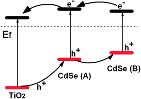
Fig. 4 shows the IPCE spectra of cells A–C at 100 mW cm−2 (AM 1.5G). It can be seen that the IPCE peaks of cells A and B match the first exciton absorption as shown in Fig. 1 exactly. After sensitizing with two sizes of CdSe QD, a slight red shift and broadening of the peak indicates an increase in the electronic coupling between the CdSe QDs, which can facilitate exciton delocalization and motion through the CdSe QD film.14 Meanwhile, the enhanced IPCE observed in cell C compared to cell B can be attributed to the elevation of the conduction band edge of CdSe II via band alignment between CdSe I and II. The increased potential difference between CdSe II and TiO2 would facilitate electron separation and transfer from CdSe II to the TiO2 film and thereby improve the IPCE. This phenomenon was also observed in a CdSe/CdS/TiO2 film as reported previously.15 Therefore, an IPCE of 26% is achieved for cell C. The inset of Fig. 4 shows photographs of the photoelectrodes for cells A, B, and C with the color changing from orange to red in good agreement with the absorption spectra (Fig. 1).
 | ||
| Fig. 4 IPCE spectra of cells A–C measured in polysulfide electrolyte. The inset shows photographs of the TiO2/CdSe I, TiO2/CdSe II, and TiO2/CdSe I/CdSe II photoelectrodes. | ||
Fig. 5 shows the J–V characteristics of cells A–C. The parameters of the performance of the QDSSCs taken from the J–V characteristics are shown in Table 1. From Fig. 4, it can be seen that the PCE increases from 0.53% (cell A) to 1.26% (cell C) mainly due to the short-circuit current density (Jsc) increasing from 2.25 mA cm−2 (cell A) to 3.41 mA cm−2 (cell C), consistent with the IPCE trend in Fig. 4. The higher Jsc most likely results from enhanced light harvesting due to the broader light absorption for the co-sensitized QDSSC. Meanwhile, the fill factor (FF) of cell C is largely improved compared to cells A and B, indicating a good capability of inhibiting the charge recombination at the TiO2/electrolyte interface, as a result of the good QD coverage of the TiO2 film.
 | ||
| Fig. 5 J–V characteristics of cells A–C measured under simulated solar illumination (AM 1.5G) with an intensity of 100 mW cm−2 in polysulfide electrolyte. | ||
Lastly, to reveal the interfacial reactions of photoexcited electrons in the QDSSCs, we measured EIS spectra of as-prepared QDSSCs. Fig. 6(a) shows the Nyquist plots of QDSSCs using cells A–C at an applied bias of Voc and a frequency range from 10−1 Hz to 106 Hz, with an AC amplitude of 10 mV under the illumination of one Sun (AM 1.5G, 100 mW cm−2). Two semicircles are observed in the high-frequency region (>1 kHz) and middle-frequency region (10–100 Hz), respectively. It was reported that the middle-frequency peak reflects the properties of the photoinjected electrons with the oxide semiconductor.16 Under Voc conditions, the electrons injected into the oxide semiconductor should be recombined at the oxide/dye/electrolyte interface because there is no current passing through the external circuit.17 Thus the lifetime of electrons in the oxide film (τr) can be estimated according to the equation: τr = 1/(2πfmax), where fmax is the maximum frequency of the mid-frequency peak.16 As shown in Fig. 6(b), the fmax value for cell C is 10.5 Hz, smaller than the value for cell A (24.3 Hz) and cell B (26.0 Hz). Therefore, the electron lifetimes are calculated to be 6.5, 6.1 and 15.2 ms for cells A, B and C, respectively. The longer electron lifetime for cell C indicates more effective suppression of the back reaction between photoelectrons in the conduction band of TiO2 and the electrolyte.18 It is possibly due to the better coverage of the TiO2/CdSe I/CdSe II photoelectrode, which inhibits the surface recombination of electrons at the electrode/electrolyte interface. As a result, the longer electron lifetime enables cell C to achieve a higher solar cell efficiency.
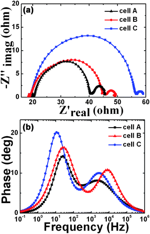 | ||
| Fig. 6 (a) Nyquist plots of QDSSCs of cells A–C. (b) Bode phase plots of cells A–C. | ||
4. Conclusion
We have fabricated a QDSSC based on two sizes of CdSe QD. The improved performance of the TiO2/CdSe QD (2.5 nm)/CdSe QD (3.5 nm) cell is mainly due to the increased Jsc and FF, which is attributed to its broader light absorption range and a longer electron lifetime. As a result, a PCE of 1.26% was achieved for our device using two sizes of CdSe QD.Acknowledgements
The authors are grateful for the financial support of the National Science Foundation of China (No: 50872022, 60801002, 60971017), National Key Basic Research Program 973(2010CB327705), the Chinese 111 project (B07027), the “863” Program of China (2007AA01Z303, 2008AA03A314), NSF Project of Jiangsu province (BK2009264), the Research Fund for International Young Scientists from NSFC (51050110142) the Scientific Research Foundation of the Graduate School of Southeast University (YBJJ1002), and the “Talent-100” program of the Chinese Academy of Science.References
- P. V. Kamat, J. Phys. Chem. C, 2008, 112, 18737 CAS.
- Y. L. Lee and Y. S. Lo, Adv. Funct. Mater., 2009, 19, 604 CrossRef.
- D. H. Cui, J. Xu, T. Zhu, G. Paradee, S. Ashok and M. Gerhold, Appl. Phys. Lett., 2006, 88, 183111 CrossRef.
- X. F. Gao, H. B. Li, W. T. Sun, Q. Chen, F. Q. Tang and L. M. Peng, J. Phys. Chem. C, 2009, 113, 7531 CrossRef CAS.
- R. D. Schaller, V. M. Agranovich and V. I. Klimov, Nat. Phys., 2005, 1, 189 CrossRef CAS.
- C. H. Chang and Y. L. Lee, Appl. Phys. Lett., 2007, 91, 053503 CrossRef.
- A. J. Nozik, Inorg. Chem., 2005, 44, 6893 CrossRef CAS.
- W. Shockley and H. J. Queisser, J. Appl. Phys., 1961, 32, 510 CAS.
- G. A. Zhu, Z. J. Cheng, T. A. Lv, L. K. Pan, Q. F. Zhao and Z. Sun, Nanoscale, 2010, 2, 1229 RSC.
- I. Mora-Sero, S. Gimenez, F. Fabregat-Santiago, R. Gomez, Q. Shen, T. Toyoda and J. Bisquert, Acc. Chem. Res., 2009, 42, 1848 CrossRef CAS.
- W. Lee, S. H. Kang, S. K. Min, Y. E. Sung and S. H. Han, Electrochem. Commun., 2008, 10, 1579 CrossRef CAS.
- J. Chen, D. W. Zhao, J. L. Song, X. W. Sun, W. Q. Deng, X. W. Liu and W. Lei, Electrochem. Commun., 2009, 11, 2265 CrossRef CAS.
- W. W. Yu, L. H. Qu, W. Z. Guo and X. G. Peng, Chem. Mater., 2003, 15, 2854 CrossRef CAS.
- E. Talgorn, R. D. Abellon, P. J. Kooyman, J. Piris, T. J. Savenije, A. Goossens, A. J. Houtepen and L. D. A. Siebbeles, ACS Nano, 2010, 4, 1723 CrossRef CAS.
- G. M. Wang, X. Y. Yang, F. Qian, J. Z. Zhang and Y. Li, Nano Lett., 2010, 10, 1088 CrossRef CAS.
- R. Kern, R. Sastrawan, J. Ferber, R. Stangl and J. Luther, Electrochim. Acta, 2002, 47, 4213 CrossRef CAS.
- J. F. Qian, P. Liu, Y. Xiao, Y. Jiang, Y. L. Cao, X. P. Ai and H. X. Yang, Adv. Mater., 2009, 21, 3663 CrossRef CAS.
- W. Zhang, R. Zhu, X. Z. Liu, B. Liu and S. Ramakrishna, Appl. Phys. Lett., 2009, 95, 043304 CrossRef.
| This journal is © The Royal Society of Chemistry 2011 |