Controlled synthesis of ultra-long AlN nanowires in different densities and in situ investigation of the physical properties of an individual AlN nanowire
Fei
Liu
,
Z. J.
Su
,
F. Y.
Mo
,
Li
Li
,
Z. S.
Chen
,
Q. R.
Liu
,
J.
Chen
,
S. Z.
Deng
and
N. S.
Xu
*
State Key Laboratory of Optoelectronic Materials and Technologies, Guangdong Province Key Laboratory of Display Material and Technology, School of Physics and Engineering, Sun Yat-sen University, Guangzhou, 510275, P. R. China. E-mail: stsxns@mail.sysu.edu.cn
First published on 22nd November 2010
Abstract
The controlled synthesis of different growth densities of ultra-long AlN nanowires has been successfully realized by nitridation of Al powders for the first time. These AlN nanowires have an average diameter of about 100 nm and their mean length is over 50 μm. All the synthesized ultra-long nanowires are pure single crystalline h-AlN structures with a growth orientation of [0001]. We preferred the self-catalyzing vapor–liquid–solid (VLS) mechanism to illustrate their growth process. Although the sample with the middle growth density (3.2 × 10⁷ per cm2) of AlN nanowire performs the best field emission (FE) properties, the emission uniformity is not good enough for field emission display applications, which may be attributed to their low intrinsic conductivity. Moreover, the electrical transport and FE properties of an individual ultra-long AlN nanowire are further investigated in situ to find the decisive factor responsible for their FE behaviors. An individual AlN nanowire is observed to have a mean 1 nA field of 440 V μm−1 and 1 μA field of 480 V μm−1 as well as an average electrical conductivity of about 2.7 × 10⁻⁴ Ω−1 cm−1, which is lower than that of some cathode materials with excellent FE properties. Therefore we come to the conclusion that the electrical conductivity of the AlN nanowire must be improved to a higher level by some effective ways in order to realize their practical FE device applications.
Introduction
There has been a growth of interest in the potential application of various kinds of nanostructures in nanoelectronics. Among the nanomaterial candidates, AlN nanostructures have aroused significant interest in the past few years because of their excellent properties, such as high thermal conductivity (K ∼ 320 W m−1 K−1), low electron affinity (∼0.6 eV) and high melting point (over 2300 °C).1–4 Their potential applications in nanoelectronic devices have not been well explored though their field emission characteristics have been investigated for the application of vacuum nanoelectronic devices.5–9 One expects that AlN nanostructures with low electron affinity should have a rather low turn-on field, but the field emission results of AlN nanostructure films typically show a turn-on field of 4–6 V μm−1, which is higher than that of MoO2 and W18O49 (their turn-on fields are typically 2.2 and 2.0 V μm−1, respectively).10,11 What leads to their poor performance in field emission (FE) is not yet clear, which makes it hard for researchers to enhance the FE properties of AlN nanostructures and has limited their rapid development in practical applications to a great extent. One possibility is their low conductivity, which has not yet been investigated in experiment. Moreover, the electrical conductivity is also a basic consideration for other potential nanoelectronic applications and can be only measured by studying individual AlN nanostructures. The second possibility is that the aspect ratio of the AlN nanostructures is too low. Much effort has been devoted to preparing different morphologies of AlN nanostructures (nanocones, nanorods and nanowires), but there are few reports on the controlled growth of the AlN nanostructures with higher aspect ratios (< 100). Until now, the reported AlN nanostructures usually possess a lower field enhancement factor, i.e., weaker ability to magnify an applied field.5–9 The third possibility is the field screening effect due to high density of the AlN nanostructures, as found in other nanostructures,12,13 which will do harm for field electron emission.In comparison with other synthesis methods, thermal nitridation of Al powders is more simple and cheap, making it easy to fabricate mass production of AlN nanostructures on the substrate. Moreover, the whole reaction process does not produce any harmful gas or byproducts, which is beneficial for protecting the environment. Therefore here it is used to prepare ultra-long AlN nanowires. We report on the controlled growth of ultra-long AlN nanowires in different densities for the first time by the thermal nitridation of Al powders. They are investigated by SEM and TEM techniques in order to analyze their morphological and structural characters and their growth mechanism is discussed. In addition, the field emission properties of different densities of ultra-long AlN nanowires are compared together to explore the possible FE mechanism, which results in their different FE properties. In situ electrical conductivity and FE property measurements are performed on individual AlN nanowires to find the possible factors which affect their FE behaviors.
Experimental
Different densities of ultra-long AlN nanowires were successfully synthesized by adjusting the reaction time and the mixed ratio of Al powders to Fe2O3 powders. The chemical evaporation deposition system has been described in our recent reports.14–16 Firstly, hydrogen gas was used as carrier gas at the flow rate of 200 sccm when the temperature of the central reaction region arrived at 700 °C. This step lasted for 30 min, which is very important for the formation of Al nanoparticle film. Secondly, when the temperature was further raised to 1000–1200 °C, the mixed gas consisting of N2 and NH3 with a flow rate ratio of 200 sccm to 20 sccm was introduced into the vacuum chamber. The growth pressure was 50 Torr and the rising rate was 10 °C min−1 in this step. Finally, the reaction chamber was cooled to room temperature in N2 gas after a growth time of 2–8 h. The rapid rate of raising the temperature, high growth pressure and large total mass of source materials in our experiment can be helpful for the formation of ultra-long AlN nanowires, which can provide enough AlN vapors in the evaporation process. Hence, ultra-long AlN nanowires can be obtained on the substrate.A field-emission type scanning electron microscope (XL-SFEG SEM, FEI Corp.) was used to investigate the morphological characters of ultra-long AlN nanowires. Transmission electron microscopy (Tecnai-20 TEM, PHILIPS) techniques and X-ray diffraction (XRD) (Rigaku RINT 2400) techniques were employed to confirm their crystalline structures. Measurements on the field emission properties of AlN nanostructures in different growth density were performed on the field emission analysis system. In situ measurement on individual ultra-long AlN nanowire is performed in the modified SEM system (JEOL-6380).
Results and discussion
By varying the experimental conditions, we prepared different growth densities of ultra-long nanowires. For simplification, we denoted the sample with the lowest density as Sample I, the sample with a slightly higher density as Sample II and the sample with the highest density as Sample III, respectively.The SEM images of the three samples with different growth density are shown in Fig. 1, and their growth conditions can refer to Table I. It is seen in Fig. 1A that the synthesized ultra-long AlN nanowires are randomly distributed over the substrate and their growth density is very low (2.5 × 10⁶ per cm2) for Sample I. From the inset, the nanowires are seen to have a mean diameter of 100 nm and an average length of 20 μm. These nanowires stand on the substrate with an angle of about 60° and their diameter gradually decreases along their growth direction, as seen in Fig. 1B. The top-view and side-view images of Sample II are provided respectively in Fig. 1C and 1D. In comparison with Sample I, Sample II possesses a higher growth density (3.2 × 10⁷ per cm2). Although the nanowires in Sample II are longer than Sample I, they possess a diameter and shape very similar to Sample I. The ultra-long nanowires in Sample II nearly stand vertically on the substrate, as shown in Fig. 1D. The top-view and cross-section SEM images of Sample III are given in Fig. 1E and 1F. It is clearly seen that Sample III has the highest growth density (7.1 × 10⁷ per cm2) of AlN nanowires among these samples, as seen from Table I. Moreover, the nanowires in Sample III have the largest diameter of about 200 nm on the top, as shown in the inset. To better understand the growth mechanism, the growth time of AlN nanowire is altered to be 20 min. The white cross and circle in Fig. 1G are the respective measurement regions of the EDX spectra (Fig. 1H and 1K). It is obviously seen in Fig. 1Gthat the bottom of the AlN nanowires are located on a layer of thin film, which proposes that a thin film on the substrate may play a key role in the formation of these nanowires. In order to further analyze their compositions, we compared the microscale EDX spectrum of the AlN nanowire with that of the thin film in Fig. 1H and K. It is found that only elements Al and Si can be detected for the thin film, which is different from the spectrum of the nanowire (elements Al and N). Element Si may come from the silicon substrate, so it is concluded that the thin film on the substrate should be an Al film. From these SEM images, it is calculated that the aspect ratio of the synthesized ultra-long AlN nanowires reaches 250–500. It suggests that they should be more suitable for applications in the FE area.
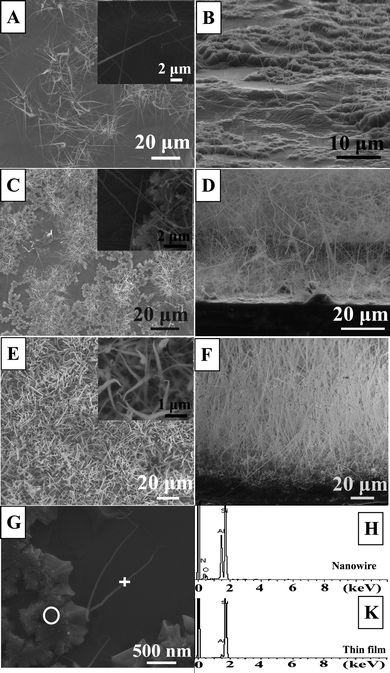 | ||
| Fig. 1 (A) Top-view and (B) side-view SEM images of the ultra-long AlN nanowires with the lowest density (Sample I). The inset in Fig. 1A is the high magnification image of Sample I. (C, D) Top-view and side-view SEM images of the ultra-long AlN nanowires (Sample II) with lower density, respectively. The inset in Fig. 1C is the high magnification image of Sample II. (E, F) Top-view and side-view SEM images of the ultra-long AlN nanowires (Sample III) with the highest density, respectively. The high magnification image of Sample III is in the inset in Fig. 1E. (G) The SEM images of ultra-long AlN nanowire at initial growth stage of 20 min. (H, K) The EDX spectrum corresponding to the marks in image (G). | ||
To confirm the chemical compositions of the products, an XRD technique was first applied to these three samples; Fig. 2 gives the typical XRD patterns. It is seen that these samples are well-crystallized and exhibit three characteristic peaks of the AlN phase with a wurtzite structure, which correspond to the data of the Joint Committee for Powder Diffraction Standards (JCPDS) card No. 25-1133. Moreover, it is observed that the intensity of the (001) diffraction peak of Sample III is stronger than other two samples, which suggests the alignment of ultra-long AlN nanowires in Sample III is the best in three samples. In addition, only the diffraction peaks of the AlN phase can be found and no Si characteristic exists in the pattern for Sample III, which shows that Sample III possesses the highest growth density of ultra-long AlN nanowires among the three samples. It is also seen that the Al peaks can be found in the XRD pattern of Sample I, which indicates that some remaining Al film exists on the surface of the substrate. The Al film may result from the remained Al nanoparticle film after the reaction and the detailed reason will be discussed in the section relating to their growth mechanism. Because the reaction times (4 h and 8 h) are longer for Sample II and III, the Al film formed on the surface of Si substrate at initial stage should have been already consumed in the growth process. Therefore there are no Al signals in their XRD patterns, which is different from Sample I.
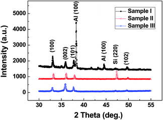 | ||
| Fig. 2 Typical XRD patterns of the three kinds of ultra-long AlN nanowires. | ||
In order to research the crystalline structure of ultra-long AlN nanowires, TEM and EDX techniques were performed on these three samples. Through detailed investigations, it is found that the synthesized AlN nanowires have nearly the same crystalline structures no matter what their density is, so we only provide a typical TEM image of ultra-long AlN nanowires, as shown in Fig. 3A. It is seen in Fig. 3A that the ultra-long AlN nanowire has a coarse shape and exhibits a multi-layer structure. The top diameter of the nanowire is about 100 nm, which is consistent with our SEM results. From the HRTEM image of the nanowire (shown by the white circle in Fig. 3A) in Fig. 3B, the AlN nanowire is observed to have a mean lattice spacing of 0.26 nm between two adjacent crystalline planes. The growth direction of the nanowire is [001] based on the JCPDS card No. 25-1133. The corresponding selected area electron diffraction (SAED) pattern is in the inset, in which one can see that the diffraction spots are clear and sharp. Moreover, the HRTEM image is atom-resolved and no defects can be found, which suggests that the as-prepared ultra-long AlN nanowires are single crystals with a wurtzite structure. We further carried out the electron energy loss spectroscopy (EELS) technique to reveal their elemental compositions. From Fig. 3C and D, only the Al L1, L2 and L3-edge peaks and N k-edge peak appear in the spectrum. Gatan EELS analysis also indicates that the total content of element Al and N is over 96%, thus it proves that these samples are pure AlN single crystals. To further confirm the compositions of a single AlN nanowire, EDX technique is performed on the bottom and the middle of the nanowire, as shown in Fig. 3E. By comparison of the EDX spectrum (Fig. 3F), it is found that there is some Si in the spectrum of the bottom and the middle of the nanowire, which suggests that Si has been doped into the nanowire. Moreover, through the quantitative EDX analysis, the content of Si in the nanowire is ranging from 2% to 4%, which proposes that Si is the main dopant in the nanowire. Fig. 3G and H provide the TEM and HRTEM images of the tip of the AlN nanowire to further investigate their crystalline structure. The atom-resolved images can be clearly observed in Fig. 3H and there are no obvious defects in their high resolution images. Therefore we come to the conclusion that the tip of the nanowire has almost the same single crystalline structure as the middle of the nanowire, which implies that they have good crystallinity.
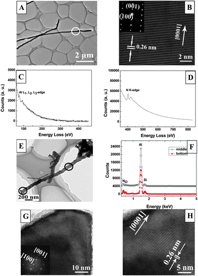 | ||
| Fig. 3 (A) Typical TEM image of ultra-long AlN nanowire. (B) The atom-resolved enlarged image of the sample, which comes from the section of the ultra-long nanowire referred to the white circle in Fig. 3A. The inset is the corresponding SAED pattern. (C, D) The corresponding EELS spectrum of the nanowire, which respectively exhibits the characteristic absorption peaks of element Al and N. (E, F) The EDX spectrum from the middile and the bottom of an individual AlN nanowire, respectively. (G, H) The TEM and HRTEM image of the tip of the ultra-long AlN nanowire, respectively. The inset is the SAED pattern of the tip. | ||
To better understand the effect of the experimental conditions on the growth density of the ultra-long AlN nanowires, we summarized their morphological characters in Table 1. By analyzing this table, we found that the ratio of source materials is essential for the fabrication of ultra-long AlN nanowires. It is not difficult to understand because the smaller the ratio of Fe2O3, the fewer Al atoms evaporate at high temperature, which must induce a lower density of Al nanowires forming on the substrate in the following reaction process. It is also seen that if the total mass of the source materials is adjusted to be smaller, their growth density can become lower. At the same time, the growth time has some effects on the morphology of AlN nanowire. As shown in Fig. 1, the length of the AlN nanowire will gradually become longer with the increase of the growth time to 4 h. When the growth time is over 4 h, almost no change is found for the length of nanowires and only their diameter is found to grow continuously. However, when the ratio of Al powders to Fe2O3 powders is altered to be higher than 8 : 1, ultra-long AlN nanowires are hard to synthesize even if the growth time is adjusted to be 20 h or longer, which proves that the source material ratio is the determining factor in the formation of the nanowires.
According to a series of experiments and analysis, we prefer the self-catalyzing Vapor–Liquid–Solid (VLS) mechanism17,18 to explain the growth of ultra-long AlN nanowires because no catalysts were used in this experiment. The schematic diagram of the growth process is depicted in Fig. 4. Firstly, the Al powders turn to be in liquid phase due to their low melting point of about 650 °C. They can react with Fe2O3 powders in this situation, and should obey the following equation:19–21
| 6Al(l) + Fe2O3(s) → 3Al2O(g) + 2Fe(s) | (1) |
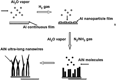
In this step, the existence of Fe2O3 powders can effectively lower the synthesis temperature of Al2O vapor and promote the formation mass of the Al source vapors to some extent according to the reports in ref. 20. Secondly, the Al2O vapor is transferred to the surface of substrate and reacts with hydrogen gas to form an Al thin film based on eqn (2):
| Al2O(g) + H2(g) → 2Al(s) + H2O(g) | (2) |
It can be also proven by the existence of element Al in the XRD pattern of Sample I (Fig. 2) and the EDX spectra of the initial growth stage of AlN nanowire (Fig. 1H and K). Subsequently, with the function of H2 gas, the continuous film gradually separates into Al nanoparticle film, which is similar to the process proposed in ref. 22 and 23. Thirdly, when the temperature is increased to 1000 °C, NH3 gas is introduced into the vacuum chamber and the following reactions are described in eqn (1), (3) and (4):
| Al2O(g) + 2NH3(g) → 2AlN(s) + H2O(g) + 2H2(g) | (3) |
| 2Al(l) + 2NH3(g) → 2AlN(s) + 3H2(g) | (4) |
At a high temperature of 1000 °C, Al nanoparticle precursors exist in the liquid phase on the substrate and can be the nucleus for the absorbing foreign atoms because of their high surface energy. So the foreign N atoms react with the Al liquid droplets to form the AlN precursors while the Al2O vapor reacts with NH3 to synthesize AlN molecules, i.e., these three reactions occur at the same time. These AlN solids obtained from the above reactions continuously resolve into the Al droplets as the reactions proceed. When the solubility of AlN precursors in Al droplets reaches oversaturation, AlN solids begin to separate from oversaturated solutions and form the seeds for the growth of the nanowire. Fourthly, the supplement vapor from the reaction region gradually absorbs on these seeds and grows along the [0001] preferred orientation at a rapid growth rate. Of course, the size or the surface properties of the original seeds also takes some effect on the morphology of the nanowire as illustrated in ref. 24, which can be determined by the flow rate of H2 and the growth pressure in our experiment. Finally, high density of ultra-long AlN nanowires are synthesized on the substrate. In this growth process, Si may play a role in inducing the formation of the alloy catalyst droplets based on one group’s report.19,21 However, by investigation of the TEM image and the EDX spectrum (Fig. 4), it cannot be directly confirmed because element Si exists in the whole nanowire, so a further detailed investigation into their growth mechanism is undergoing.
The field emission measurements on three samples were carried out in the field emission analysis system and the base pressure in the vacuum chamber was lower than 3 × 10⁻⁷ Pa. To measure the FE properties of these three samples, the transparent anode method was used in the measurements. These three samples were used as the cathode and the indium-tin-oxide (ITO) glass was used as the anode. The area of the samples was around 3 × 2 cm2 and the vacuum gap distance between anode and cathode was about 400 μm. The emission current density versus electric field (J–E) curves and Fowler–Nordheim (FN) plots of three samples are given in Fig. 5A and 5B, respectively. To compare their FE behaviors, the detailed FE property data of three samples are summarized in Table 2. As seen in Table 2, Sample II with lower density of ultra-long AlN nanowires has the lowest turn-on field of 4.5 V μm−1 (J = 10 μA cm−2) and the lowest threshold field of 10.4 V μm−1 (J = 1 mA cm−2) among three samples. The FE properties of the ultra-long AlN nanowires seems to be worse than those of the Si-doped AlN nanowires in other groups.25 The possible reasons are summarized as the following. The FE behavior measured in the cathode microprobe method is usually much higher than the obtained results in the transparent anode method because the FE measurement only focuses on a small emission area under the microprobe for the cathode microprobe method; this is the main reason for the discrepancy. However, the transparent anode method is dedicated to measure the FE behaviors of the whole film rather than a small emission area, which is more suitable for valuing the FE performance of nanostructured film in FE applications. So here we applied this measurement method to investigate our samples. Also, the existence of higher content of Si dopants and the smaller top diameter of the nanowire in recent reports than our synthesized nanowire should have some effect on the difference of their FE behaviors.
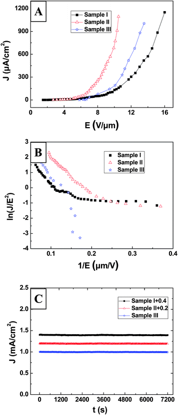 | ||
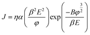
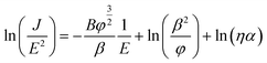
| Fig. 5 (A) The J–E curves of ultra-long AlN nanowires of three densities. (B) Their corresponding FN plots. (C) Their emission stability curves. | ||
| Sample | FE properties | |||
|---|---|---|---|---|
| Turn on field at 10 μA cm−2/V μm−1 | Threshold field at 1 mA cm−2/V μm−1 | β (enhancement factor) | η (geometrical efficiency of FE emission) | |
| Sample I | 4.8 | 15.5 | 1138 | 0.66% |
| Sample II | 4.5 | 10.4 | 1997 | 7.79% |
| Sample III | 6.5 | 13.3 | 1391 | 2.54% |
It is also found in Fig. 5B that their FN plots are all deviated from linearity. Based on the classical Fowler–Nordheim (FN) theory,26 the relationship between current density J and applied field E should be described as follows:
 | (5) |
It is clear that the three samples with different nanowire densities exhibit different FE behaviors, as seen in Fig. 5 and Table 2. To explore the field emission mechanism that arouses the discrepancy is very crucial because it can provide a guidance to find the most suitable growth conditions of AlN nanowire for practical FE device applications. It is clearly seen that the growth density of Sample I is the lowest (2.5 × 10⁶ per cm2), that of Sample II is lower (3.2 × 10⁷ per cm2) and that of Sample III is the highest (2.1 × 10⁸ per cm2) among three samples. Sample II and Sample III should have better FE performances than Sample I because there are more emitters existed on a given unit area of the sample. The aspect ratio of Sample III is observed to be slightly larger than that of Sample I, but the growth density of Sample III is almost 102 times larger than that of Sample I. Then the FE properties of Sample III is better than Sample I as seen in Table 1, which suggests that the growth density of the emitters should be dominant for these two samples in comparison with the aspect ratio. However, as observed in Table 2, Sample II with lower growth density has better FE properties than Sample III with the highest density, and thus the field screening effect must be considered10,11 in this situation. According to this theory, the surface of the nanostructured film of high density is very much like a plane surface. When the field is applied between the anode and the cathode, it will prevent the macroscopic electric field from penetrating into the nanostructure film,10 which thus lowers the local field amplification existing among the nanostructures and makes electron emission hard to occur. It is obvious that the higher the density of nanowire, the greater the role that the field screening effect plays in the actual field emission process. Therefore it is concluded that the field screening effect of Sample III is the most distinguished among these three samples because of the highest nanowire density. Therefore, it is reasonable that Sample III should have worse FE behaviors than Sample II, which is in good agreement with our observed results given in Fig. 5. Combined the field screening effect in emission process with the nonlinearity of their FN plots, the Filip model should be more appropriate for illustrating the mechanism of these samples.28
In addition, the geometrical efficiency of electron emission η needs to be obtained because of the requirement of qualitatively investigating of the field screening effect. To calculate the value of η, eqn (6) may be derived as follows:
 | (6) |
Based on eqn (6), the corresponding η value can be obtained for three samples, as indicated in Table II. It is obviously seen in Table II, Sample II has the highest η value (7.79%) in the equal applied field, which suggests that Sample II has the largest number of effective emitters existing under the same applied field in comparison with other two samples. Therefore, Sample II should have the best FE behaviors among three samples, which conforms to our observed results in Fig. 5. Moreover, it is observed that the emission efficiency for three samples is not very high, which implies that not all AlN nanowires are involved in field emission process because some non-uniformity of the nanowires exists in the samples.
The emission stability of the samples are also explored, which is essential for valuing the feasibility of the ultra-long AlN nanowires in FE applications. Their emission stability curves are shown in Fig. 5C. The whole measurement lasted 2 h, and the initial emission current density was kept at 1 mA cm−2 for these three samples. It is seen that the current fluctuation of all the samples is lower than 6% throughout the measurement, which is good enough for practical FE applications. It is also found that these three samples have similar field emission stabilities and they can endure a high current density for a long period.
However, from the obtained results given in Table 2, all three samples with different densities fail to exhibit excellent FE performances, such as their high turn-on field, high threshold field and some emission uniformity, which are not good enough to meet the application requirements of FE devices. One of the factors leading to their FE behaviors is probably the low electrical conductivity of the AlN nanostructure. In order to confirm this, measurement of the individual AlN nanowire is very essential because many pieces of physical information of AlN nanowire are concealed by the continuous film due to some effects. Few reports so far are concerned with the characterization of individual single AlN nanowires because the AlN nanowires are often prepared in high density, which is hard to carry out for in situ measurement on individual nanowires. Since we have mastered the controlled growth technique of the AlN nanowire with different densities, measurement of the physical properties of an individual nanowire becomes feasible. The measurement was carried out in a modified SEM system, which has been depicted in detail in our previous papers.16,29,30Fig. 6A and 6B provide the SEM images of the W probe and a single AlN nanowire during electrical conductivity measurement and field emission measurement, respectively. It is seen from Fig. 6A that the W probe tightly contacts to individual ultra-long AlN nanowire on its end. Individual nanowire has a length of about 50 μm and a diameter of about 100 nm, which is consistent with the observed images in Fig. 1. One can see in Fig. 6B that the distance between the W probe and individual nanowire was kept at about 2 μm through field emission measurement. In order to eliminate possible influence from other nanowires and ensure the accuracy of the measurement, a series of treatments have been done before the measurement on the individual nanowire. Firstly, the sample with low-density nanowires was chosen to easily confirm the accurate site of the nanowire on the substrate and make fewer nanowires exist around the measurement nanowire. Secondly, some nanowires near to the measurement nanowire have all been removed by the substrate through using the W probe to ensure the isolation of the nanowire. This step is easy to do because the movement of the W probe is facile to be controlled by the stepped-motor and the number of the nanowires near the measurement nanowire is very small. Thirdly, the tungsten probe is moved to contact an individual nanowire, which is adopted to ensure the alignment in FE measurement as well as the Ohmic contact between the probe and the nanowire during the measurements.
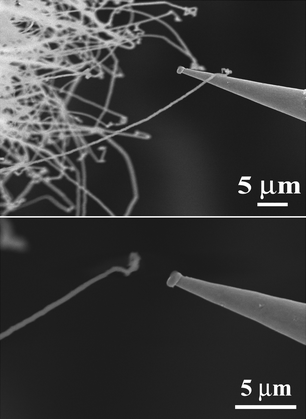 | ||
| Fig. 6 (A, B) The SEM images of individual AlN nanowire and the tungsten probe (A) during the conductivity measurement, and (B) during the field emission measurement. | ||
Representative curve of the electrical transportation property of individual AlN nanowire is shown in Fig. 7A. Here only a typical I–V curve of a single nanowire is given because their electrical conductivities are very close. It is found that they have the same order of electrical conductivity (in the range from 2 × 10⁻⁴–7 × 10⁻⁴ Ω−1cm−1) in many experiments. From the shape of the I–V curve in Fig. 7A, it can be concluded that the electric contact in conductivity measurement should be the Schottky barrier rather than the ohmic contact because it is nonlinear and asymmetrical. We use the following descriptions to explain this phenomena. The total resistance RTotal consists of the contact resistance RContact and the intrinsic resistance RAlN of AlN nanowire. The contact resistance in measurements can be divided into two types, i.e., the contact resistance R1 between the nanowire and the substrate and the contact resistance R2 between the nanowire and the W probe. It means that the expression of the total contact resistance can be written as RTotal = RAlN + RContact = RAlN + R1 + R2. The work functions of W, AlN and n-doped Si are usually 4.5 eV, 3.8 eV and 4.2 eV, respectively. At high growth-temperature over 1100 °C, the AlN clusters and n-doped Si will be alloyed together, which suggests that their contact resistance R1 is very low close to ohmic contact after the growth. However, for R2, high contact resistance will occur because their large discrepancy of the work function between W probe and individual AlN nanowire, which results in the formation of Schottky barrier. In this situation, R2 determines the contact resistance RContact. Based on the thermionic emission theory,31,32 the reverse current of an ideal Schottky barrier should be at a very low level because the barrier is often elevated to a very high value at reverse voltage, and the reverse current can be negligible in contrast to their positive current at this situation. The positive current will exponentially increase with the positive voltage applied on the Schottky diode, followed by the equation:32
 | (7) |
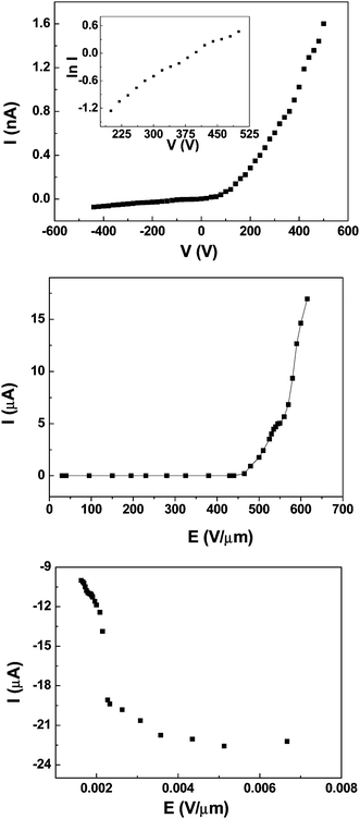 | ||
| Fig. 7 (A) Representative electrical transportation curve of a single AlN nanowire. The ln I versus V curve is in the inset. (B) The field emission I–E curves of a single nanowire. (C) The corresponding FN plots. | ||
Fig. 7B gives typical field emission current versus applied field (I–E) curve of a single AlN nanowire, and its corresponding Fowler–Nordheim (FN) plots are indicated in the inset. From Fig. 7B, individual AlN nanowire is observed to have a mean 1 nA field (defined as the electric field when the emission current is 1 nA) of 440 V μm−1 and 1 μA field (defined as the electric field when the emission current is 1 μA) of 480 V μm−1. The FE performance of the as-synthesized AlN nanowire is better than that of AlN nanocones (500 nA at 1000 V μm−1) from another group,34 which should originate from high conductivity of the individual nanowire in our synthesis process due to the doping of element Si. It is also found that the field emission current exhibits a increase tendency with the applied field and does not reach saturation until the applied field arrives at 800 V μm−1, which suggests that an AlN nanowire has a high endurance ability to large emission current because of its high thermal conductivity. The FN plots of individual AlN nanowire are seen to be nonlinear in the inset. We attributed the nonlinear behavior of the FN plots to be thedecreasee of the contact resistance R2 with the increase of the temperature followed by high applied field, because of which induces higher effective field appearing between cathode and anode. Even though it is found in Fig. 7B that the FE property of individual AlN nanowire is not very excellent in comparison with boron nanotubes,29 W18O4935etc., as we reported earlier, but this finding is consistent with the findings reported above for the FE performance of AlN nanowire films. The FE performance of a single AlN nanowire is strongly related to its low intrinsic electrical conductivity, as may be interpreted in the following. It is obvious that the intrinsic conductivity of individual AlN nanowire in our experiment is lower than that of some nanomaterials with excellent FE properties, such as CNTs (1–2 × 10³ Ω−1cm−1),36 W18O49 nanowire (10−1–10−2 Ω−1cm−1),35 ZnO nanowire (2–4 × 10⁻² Ω−1cm−1)37 and boron nanotube (10–20 Ω−1cm−1).29 So when an equal voltage is applied, more voltage drops on the nanowire's intrinsic resistance rather than falls across the vacuum gap between nanowire and anode probe, which leads to a lower effective field at the tip of the nanowire. Thus, higher applied electric field is needed for the AlN nanowire in order to realize the tunnel effects, which results in their high turn-on and threshold field. The FE properties of individual nanowire must naturally be translated to the emission performance of their corresponding film. It is known that the proper element-doping can effectively improve the electrical conductivity of individual nanostructures by forming impurity energy levels in their energy gap, which can provide enough electrons for tunnel current at lower applied field. Once the electric conductivity of individual ultra-long AlN nanowire can be enhanced to a high level (>10−2 Ω−1cm−1), they should have a more promising future in FE devices due to their low electron affinity.
Conclusions
Different densities of ultra-long AlN nanowires are controllably fabricated on the substrate by thermal nidtridation of aluminium powders. The self-catalyzing VLS mechanism is proposed to explain the growth mechanism of ultra-long AlN nanowires. The synthesized AlN nanowires are all single crystalline wurtzite structures with a length of about tens of micrometres. AlN nanowire film with a moderate density of 3.2 × 107 cm−2 exhibits the best FE performance compared to other samples, which has a turn-on field of 4.5 V μm−1 (J = 10 μA cm−2) and threshold field of 10.4 V μm−1. Moreover, taking a measurement on the individual nanowire shows that individual AlN nanowire has a lower electric conductivity (2.7 × 10⁻⁴ Ω−1cm−1) and its FE performance (1 nA field of 440 V μm−1 and 1 μA field of 480 V μm−1) is not good enough for FE applications. The former is proven to be responsible for their FE performance through our experiment. It suggests that if they want to be practically applied in high-power FE devices, the source of an electron gun or surface acoustic wave devices, the electrical conductivity of individual AlN nanowires should be further improved to a higher level by some effective ways, such as element doping.Acknowledgements
This work is supported by the National Basic Research Program of China (973 Program, Grant No. 2007CB935500; 863 Program, Grant No. 2007AA03Z305; Science Foundation, Grant No. 50802117, 51072237), the National Joint Science Fund with Guangdong Province (Grant No. U0634002, U0734003), the Foundation of Education Ministry of China (Grant No. 20070558063, 09lgpy28), the Science and Technology Department of Guangdong Province, the Education Department of Guangdong Province, and the Science and Technology Department of Guangzhou City.References
- R. F. Davis, Proc. IEEE, 1991, 79, 702 CrossRef CAS.
- V. V. Zhirnov, G. J. Wojak, W. B. Choi, J. J. Cuomo and J. J. Hren, J. Vac. Sci. Technol., A, 1997, 15, 1733 CrossRef CAS.
- D. Kang, V. V. Zhirnov, R. C. Sanwald, J. J. Hren and J. J. Cuomo, J. Vac. Sci. Technol., B, 2001, 19, 50 CrossRef CAS.
- I. V. Nicolaescu, G. Tardos and R. E. Riman, J. Am. Ceram. Soc., 1994, 77, 2265 CrossRef CAS.
- Q. Zhao, J. Xu, X. Y. Xu and D. P. Yu, Appl. Phys. Lett., 2004, 85, 5331 CrossRef CAS.
- C. Liu, Z. Hu, Q. Wu, X. Z. Wang, Y. Chen, H. Sang, J. M. Zhu, S. Z. Deng and N. S. Xu, J. Am. Chem. Soc., 2005, 127, 1318 CrossRef CAS.
- Y. B. Tang, H. T. Cong, Z. G. Chen and H. M. Cheng, Appl. Phys. Lett., 2005, 86, 233104 CrossRef.
- S. C. Shi, C. F. Chen, S. Chattopadhyay, Z. H. Lan, K. H. Chen and L. C. Chen, Adv. Funct. Mater., 2005, 15, 781 CrossRef CAS.
- S. C. Shi, S. Chattopadhyay, C. F. Chen, K. H. Chen and L. C. Chen, Chem. Phys. Lett., 2006, 418, 152 CrossRef CAS.
- J. Zhou, L. Gong, S. Z. Deng, J. Chen, J. C. She, N. S. Xu, R. S. Yang and Z. L. Wang, Appl. Phys. Lett., 2005, 87, 223108 CrossRef.
- J. Zhou, N. S. Xu, S. Z. Deng, J. Chen, J. C. She and Z. L. Wang, Adv. Mater., 2003, 15, 1835 CrossRef CAS.
- J. M. Bonard, N. Weiss, H. Kind, T. Stöckli, L. Forró, K. Kern and A. Châtelain, Adv. Mater., 2001, 13, 184 CrossRef CAS.
- B. P. Wang and L. S. Tong, Appl. Surf. Sci., 1996, 94–95, 101 CrossRef.
- F. Liu, Z. J. Su, W. J. Liang, F. Y. Mo, L. Li, S. Z. Deng, J. Chen and N. S. Xu, Chin. Phys. B, 2009, 5, 2016 Search PubMed.
- P. J. Cao, Y. S. Gu, H. W. Liu, F. Shen, Y. G. Wang, Q. F. Zhang, J. L. Wu and H. J. Gao, J. Mater. Res., 2003, 18, 1686 CrossRef CAS.
- F. Liu, J. F. Tian, L. H. Bao, T. Z. Yang, C. M. Shen, X. Y. Lai, Z. M. Xiao, W. G. Xie, S. Z. Deng, J. Chen, J. C. She, N. S. Xu and H. J. Gao, Adv. Mater., 2008, 20, 2609 CrossRef CAS.
- Z. L. Wang, X. Y. Wang and J. M. Zuo, Phys. Rev. Lett., 2003, 91, 185502 CrossRef CAS.
- F. Liu, P. J. Cao, H. R. Zhang, J. Q. Li and H. J. Gao, Nanotechnology, 2004, 15, 949 CrossRef CAS.
- Z. G. Chen, J. Zou, G. Liu, H. F. Lu, F. Li, G. Q. Lu and H. M. Chen, Nanotechnology, 2008, 19, 055710 CrossRef.
- Y. B. Tang, H. T. Cong, Z. M. Wang and H. M. Chen, Chem. Phys. Lett., 2005, 416, 171 CrossRef CAS.
- Z. G. Chen, L. N. Cheng, J. Zou, X. D. Yao, G. Q. Lu and H. M. Chen, Nanotechnology, 2010, 21, 065701 CrossRef.
- R. H. Yao, J. C. She, N. S. Xu, S. Z. Deng and J. Chen, J. Nanosci. Nanotechnol., 2008, 8, 3487 CrossRef CAS.
- M. Jung, K. Y. Eun, J. K. Lee, Y. J. Baik, K. R. Lee and J. W. Park, Diamond Relat. Mater., 2001, 10, 1235 CrossRef CAS.
- G. C. Xi, Y. T. He and C. Wang, Chem.–Eur. J., 2010, 16, 5184 CrossRef CAS.
- Y. B. Tang, H. T. Cong, Z. M. Wang and H. M. Cheng, Appl. Phys. Lett., 2006, 89, 253112 CrossRef.
- R. H. Fowler and L. W. Nordheim, Proc. R. Soc. London, Ser. A, 1928, 119, 173 CrossRef.
- Y. B. Li, Y. Bando and D. Golberg, Appl. Phys. Lett., 2004, 84, 3603 CrossRef CAS.
- V. Filip, D. Nicolaescu, M. Tanemura and F. Okuyama, Ultramicroscopy, 2001, 89, 39 CrossRef CAS.
- F. Liu, C. M. Shen, Z. J. Su, X. L. Ding, S. Z. Deng, J. Chen, N. S. Xu and H. J. Gao, J. Mater. Chem., 2010, 20, 2197 RSC.
- J. C. She, S. An, S. Z. Deng, J. Chen, Z. M. Xiao, J. Zhou and N. S. Xu, Appl. Phys. Lett., 2007, 90, 073103 CrossRef.
- Y. W. Heo, L. C. Tien, D. P. Norton and S. J. Pearton, Appl. Phys. Lett., 2004, 85, 3107 CrossRef CAS.
- S. M. Sze, D. J. Coleman and A. Loya, Solid-State Electron., 1971, 14, 1209 CrossRef CAS.
- J. Zheng, Y. Yang, B. Yu, X. B. Song and X. G. Li, ACS Nano, 2008, 2, 134 CrossRef CAS.
- Y. L. Li, C. Y. Shi, J. J. Li and C. Z. Gu, Appl. Surf. Sci., 2008, 254, 4840 CrossRef CAS.
- Z. L. Li, F. Liu, N. S. Xu, J. Chen and S. Z. Deng, J. Vac. Sci. Technol., B, 2009, 27, 2420 CrossRef CAS.
- H. Dai, E. W. Wong and C. M. Lieber, Science, 1996, 272, 523 CrossRef CAS.
- J. C. She, Z. M. Xiao, Y. H. Yang, S. Z. Deng, J. Chen, G. W. Yang and N. S. Xu, ACS Nano, 2008, 2, 2015 CrossRef CAS.
| This journal is © The Royal Society of Chemistry 2011 |