Miniaturized ionization gas sensors from single metal oxide nanowires†
Francisco
Hernandez-Ramirez‡
*ab,
Juan Daniel
Prades‡
*b,
Angelika
Hackner‡
c,
Thomas
Fischer
d,
Gerhard
Mueller
c,
Sanjay
Mathur
d and
Joan Ramon
Morante
ab
aInstitut de Recerca en Energia de Catalunya (IREC), E-08019, Barcelona, Spain. E-mail: fhernandez@irec.cat
bDepartament d'Electrònica, Universitat de Barcelona, E-08028, Barcelona, Spain. E-mail: dprades@el.ub.es
cEADS Innovation Works, D-81663, München, Germany
dDivision of Inorganic and Materials Chemistry, University of Cologne, D-50939, Cologne, Germany
First published on 16th November 2010
Abstract
Gas detection experiments were performed with individual tin dioxide (SnO2) nanowires specifically configured to observe surface ion (SI) emission response towards representative analyte species. These devices were found to work at much lower temperatures (T ≈ 280 °C) and bias voltages (V ≈ 2 V) than their micro-counterparts, thereby demonstrating the inherent potential of individual nanostructures in building functional nanodevices. High selectivity of our miniaturized sensors emerges from the dissimilar sensing mechanisms of those typical of standard resistive-type sensors (RES). Therefore, by employing this detection principle (SI) together with RES measurements, better selectivity than that observed in standard metal oxide sensors could be demonstrated. Simplicity and specificity of the gas detection as well as low-power consumption make these single nanowire devices promising technological alternatives to overcome the major drawbacks of solid-state sensor technologies.
Introduction
Since Seiyama et al. discovered that the electrical conductivity of metal oxides is dramatically changed by the presence of reactive gases in air; these materials have been intensively used as gas sensors due to their low cost and high compatibility with microelectronic processing schemes.1–3 Commonly, the detection mechanism of these devices is based on resistive measurements (RES) that are explained in terms of surface combustion processes, in which ionosorbed oxygen is removed from the metal oxide surface and in which electrons, initially trapped on surface oxygen ions, are re-emitted into the conduction band thus generating a sensor signal.4 As the criterion of combustibility is shared by a wide variety of potential analyte gases, this detection method provides poor selectivity, which is a serious drawback of current RES gas sensors and gas sensor arrays.5On the other hand, surface ionization (SI) is an alternative method of gas detection which also builds on analyte molecules adsorbed on hot solid surfaces. In this latter case, however, ionosorbed analyte ion species are extracted into free space by a counter electrode positioned at a short distance above the hot emitter surface.6 The foundations of this technology were studied in the past by Zandberg, Rasulev, Fujii and Morrison.7–11 Whereas these early works concentrated on noble and refractory metals as emitter materials, recent works demonstrated that their principles could be applied to SnO2 thin-films (emitter surface),12 which is the most widely employed material in the fabrication of RES metal oxide gas sensors;3 and ZnO nanowire arrays used as the field ionization anode.13 These first results clearly showed that metal oxides based SI gas sensors are feasible and that the SI response follows selectivity criteria which are dissimilar to those of the RES response.14,15 Building on this fact, mixed RES/SI detectors were investigated and it was demonstrated that such detectors are able to detect small concentrations of odorous and toxic amines in front of large concentrations of simple hydrocarbons.12,16,17 These latter devices employed thin film metal oxide materials deposited on standard ceramic heater substrates and were arranged in a parallel plate capacitor geometry to enable SI read out. Nevertheless, they had a serious technical drawback that made extremely complicated their integration in portable and energy efficient systems; high temperature operation (T ≈ 500–800 °C) and the need of large electrostatic potentials (Vc ≈ 103 V) to activate them.12,14,16,17
Working into the direction of portable, low power consumption gas sensor systems,18–20 we report here on the fabrication and electrical characterization of surface ionization gas sensors based on individual SnO2 nanowires (Fig. 1). In the following, we firstly show that these prototypes work at much lower bias voltages Vc and temperatures T than their micro-counterparts, providing a direct evidence of the intrinsic advantages of using one-dimensional nanomaterials as building blocks of SI systems. Secondly, we demonstrate that RES and SI measurements can be simultaneously obtained from single nanowires to improve the selectivity of standard metal oxide nanosensors.18,21 On the whole, our results suggest that single-nanowire based gas detection devices can significantly advance the state of the art in solid state gas sensing devices.
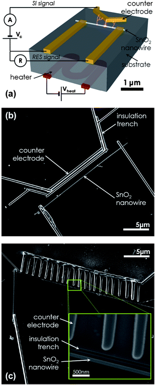 | ||
| Fig. 1 (a) Schematics of a surface ionization gas sensor. An individual SnO2 nanowire is electrically contacted directly opposite to a counter electrode. Resistive measurements (RES) are performed between the two electrodes making contact with the nanowire, whereas surface ion (SI) experiments are carried out between the nanowire and the counter electrode. The working temperature of the device was controlled by means of an external heater. (b) A scanning electron microscopy (SEM) image of a surface ionization gas sensor fabricated with FIB lithography. (c) A comb-shaped counter electrode was also made to maximize the electrical field E between it and the SnO2 nanowire. Inset: magnified SEM view of the sub-micrometre counter electrode–nanowire gap. A trench was milled in between to avoid uncontrolled leakage current contributions. | ||
SnO2 nanowires synthesized by catalyst supported chemical vapor deposition22,23 of a molecular precursor [Sn(OtBu)4] were transferred onto Si chips with pre-patterned Au/Ti/Ni microelectrodes.24,25 To avoid leakage currents through the substrate, the silicon was covered with a uniform 50 nm thick thermally grown SiO2 layer. Electrical contacts were made on SnO2 nanowires with Focused Ion Beam (FIB) lithography using an FEI Dual-Beam Strata 235 instrument combined with a trimethylmethylcyclopentadienylplatinum [(CH3)3CH3C5H4Pt] injector to deposit platinum.24,26 SI and RES measurements were made with a commercial electrometer (Keithley 6517A) and a standard Source Measure Unit (Keithley 2400), respectively. Accurate gaseous environments were maintained inside a customized test chamber with mass flow controllers mixing synthetic air (SA) and lab-class analyte gases.27,28 The effective temperature of the devices was controlled using a ceramic heater attached to the Si chip that was carrying the single-nanowire device.
As shown in Fig. 1, individual SnO2 nanowires were electrically contacted to two microelectrodes to observe their conventional RES response. Additionally, a Pt counter electrode was formed by FIB lithography directly opposite to the nanowire to observe its SI response. Several of such devices were fabricated with gap distances between nanowire and counter electrode ranging between 400 nm and 2 µm. In all cases, a trench was milled between the nanowire and the counter electrode to avoid uncontrolled leakage currents through the substrate due to the surrounding FIB's platinum halo deposited onto the chip.26,29 This last step is explained in detail in the ESI†. The final devices exhibited robust characteristics and reproducible electrical responses in different experiments repeated along several days. Provided that SI emission is enhanced with a high local electrical field E,12 the design of some prototypes was slightly modified, and comb-shaped counter electrodes were fabricated in front of the nanowires (Fig. 1c). We routinely found that these devices exhibited somewhat higher SI responses than the ones fitted with straight counter electrodes (Fig. 1b).
Fig. 2 shows the typical variation of the positive SI emission current measured between a SnO2 nanowire and the counter electrode when a hydrocarbon gas is introduced into the test chamber (1% of ethene diluted in SA). At the typical working temperatures of conventional SI devices (T ≈ 400 °C),7,12 fast and completely reversible responses were monitored with extraction voltages Vc of only a few volts. This finding entails a significant improvement compared to the macroscopic parallel-plate capacitor arrangements which had previously been used.12 In terms of extraction voltage Vc the reduction amounts to almost a factor of 1000 (∼1000 V → ∼1 V). The fact that Vc necessary to observe SI effect shifts to lower values is explained because the same local electrical field E between the nanowire and the electrode can be reached with decreasing bias voltage V if the nanowire–electrode distance d is significantly reduced (from millimetres to microns). Actually, both magnitudes E and V are related,
| E = V/d | (1) |
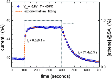 | ||
| Fig. 2 Positive surface ion (SI) emission response of the device shown in Fig. 1b towards 1% of ethene diluted in synthetic air (SA) at 400 °C. The bias voltage between the counter electrode and the nanowire was kept constant at Vc = 0.6 V. A completely reversible variation of the output current is observed after removing the target gas. The characteristic time constants of the pulse were strongly influenced by the filling/emptying dynamics of the test chamber and therefore did not represent intrinsic dynamic properties of the nanowire device. | ||
Hence, the threshold Vc value to activate SI signal, which is linked to an experimentally estimated electrical field in the nanowire–electrode gap of around E = 5 × 10⁵ V m−1, takes more reasonable values for real device design and fabrication, and provides a direct evidence of the inherent advantage of working with one dimensional nanomaterials.
Fig. 2 further shows that the gas induced signal change is roughly a few nA. Interestingly, this is the same order of magnitude of ion current responses that were observed in our previous experiments on macroscopic thin films of SnO2 (area ∼ ≈ 13 mm2) read out using a parallel plate capacitor arrangement (d = 1 mm, Vc = 103 V).17 Dividing the extracted ion currents through the geometrical cross-section of the emitting area, the current density enhancement in the nanowire devices is no less than a factor of 107 to 108. We tentatively attribute this huge enhancement to two effects:
- The huge electrical field enhancement at the nanowire surface.
- The small air gaps in the nanowire devices which approach the mean free path in the ambient air (λ ≈ 0.2 µm).30
However, the accurate analysis of the high yield of these sensors is an area where significant progress remains to be made in the future and goes beyond the preliminary description of this letter. Therefore, we will come back to a quantitative analysis of these factors in a forthcoming publication.
To rule out the possibility that the SI signal and the reference current I0 in synthetic air (SA) came from uncontrolled leakage current through the substrate, some experimental studies were performed (see ESI†). Calibration prototypes made up of two FIB-deposited Pt stripes positioned directly opposite to each other at a distance below one micron exhibited resistance values at room temperature (T = 25 °C) higher than 0.5 T Ω. Actually, current values lower than 10 pA were always monitored with an applied bias voltage of 5 V, demonstrating that leakage currents through the substrate were a second order contribution in our devices. Secondly, experiments performed with real devices at vacuum conditions demonstrated that the reference current I0 in SA, which reached values of even tens of nA in normal working conditions, tends to zero in the absence of air molecules in the counter electrode–nanowire gap. Hence, the origin of I0 was mainly put down to conduction phenomena in the gas phase, which will be studied elsewhere at a later date.
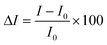
Fig. 3 shows the positive SI emission response of a SnO2 nanowire towards 0.5% and 1% of ethene diluted in SA at different working conditions. Here, SI response (ΔI) was defined as,
 | (2) |
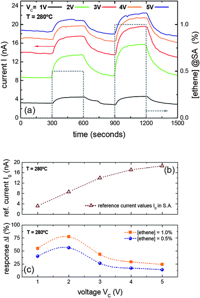 | ||
| Fig. 3 For the device shown in Fig. 1c, (a) positive surface ion (SI) emission response towards two different concentrations of ethene (0.5% and 1%) diluted in synthetic air (SA) at an operation temperature of 280 °C was observed at different Vc. (b) Reference current I0 as a function of Vc. I0 scales with Vc, reaching saturation above Vc = 3 V. (c) Response ΔI to ethene as a function of Vc. A maximum is found at Vc = 2 V. | ||
The response of some of these devices under different bias conditions Vc was also studied (Fig. 3a). The reference background current I0 was found to scale proportionally with Vc (I0 ≈ Vc) up to about Vc ≈ 3 V showing weak signs of saturation at larger potentials (Fig. 3b). The gas response ΔI displayed a complex dependence with the extraction potential Vc. Actually, Fig. 3c shows that there was an optimum Vc value for a given temperature T that maximizes ΔI. This result is crucial for the future engineering of SI nanodevices, since both T and Vc can be fixed with high precision to work at the best sensing conditions for each analyte gas.
Here, it should be pointed out that all these results were obtained at temperatures (T ≈ 280 °C) significantly lower than the ones used in macroscopic SI devices (T ≈ 800 °C),12,17 and quite close to those typical for conventional RES devices. In terms of surface temperature requirements, the temperature lowering amounts to more than ΔT ≈ 500 °C (800 °C → 280 °C). Hence, this allows integrating SI nanodevices and commercial heating solutions developed for RES-based technologies or using the self-heating effect in nanowires,19,20,31,32 paving the way to develop single nanowires based devices with a combined RES/SI readout.19,33,34
Although such mixed devices in which simultaneous RES and SI sensing can be carried out have not yet been fabricated and tested, their potential performance nevertheless has been assessed with simpler prototypes and sequential experiments. Fig. 4 shows the typical SI and RES responses of the same SnO2 nanowire towards oxidizing (NO2) and reducing (CO) pollutants. As far as RES responses are concerned, the devices behaved exactly as expected; the resistance increased in the presence of NO2 and decreased with CO. Both kinds of response are usually explained in terms of well-known gas–metal oxide interaction mechanisms.4,32,35 On the other hand, SI signal increased with NO2 and remained unchanged with CO. Positive SI currents upon exposure to oxidizing gases (NO2) cannot be explained using the theoretical models that describe RES responses of n-type metal oxides. Actually, the presence of oxidizing pollutants usually turns into an increase of the metal oxide resistance, contrary to the experimental evidence. Moreover, the lack of response of the devices towards CO is not foreseen by RES sensing principles either. In contrast, the very different SI responses towards NO2 and CO are easily explained from the SI perspective12 in terms of the vastly different ionization energies of the two molecules: 9.8 eV in the case of NO2 and 14.0 eV in the case of CO.30 Therefore, these results confirm that SI signal was monitored and vividly demonstrate that significant gains in selectivity, the real Achilles' heel of metal oxides sensors, are likely to be obtained when single-nanowire devices are configured to support simultaneous RES and SI readout modes.
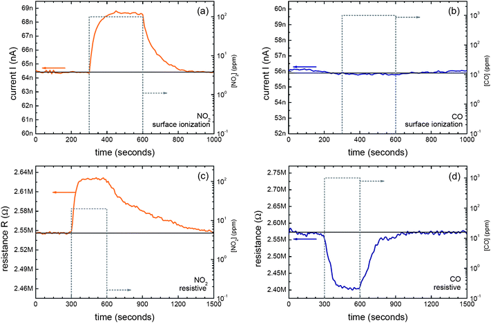 | ||
| Fig. 4 (a and b) Surface ion (SI) emission response towards NO2 and CO, respectively. Experimental conditions were fixed at Vc = 0.5 V and T = 280 °C. (c and d) Resistive response towards NO2 and CO, respectively. Experimental conditions were fixed at T = 280 °C. | ||
In summary, gas detection experiments were performed with individual SnO2 nanowires specifically configured to observe surface ion (SI) emission response towards representative analyte species. These devices significantly outperform their macroscopic counterparts, working at much lower temperatures and bias voltages and producing orders of magnitude larger ionization currents per unit emitting surface. Our gas sensing tests indicate that future single-nanowire devices with a combined RES/SI readout will enable significant gains in selectivity with regard to conventional single-response RES gas sensors.
Acknowledgements
The research leading to these results has received funding from the European Community's 7th Framework Programme under grant agreement no. 247768 (S3 Project). J. D. Prades acknowledges the support of the ‘Research stay and study visits for university academics and scientists’ program of DAAD (grant no. 314-A/10/02028).References
- T. Seiyama, A. Kato, K. Fujiishi and M. Nagatani, Anal. Chem., 1962, 34, 1502–1503 CrossRef CAS.
- E. Comini, C. Baratto, G. Faglia, M. Ferroni, A. Vomiero and G. Sberveglieri, Prog. Mater. Sci., 2009, 54, 1–67 CrossRef CAS.
- G. Korotcenkov, Mater. Sci. Eng., B, 2007, 139, 1–23 CrossRef CAS.
- N. Barsan, D. Koziej and U. Weimar, Sens. Actuators, B, 2007, 121, 18–35 CrossRef.
- G. Korotcenkov, Mater. Sci. Eng., R, 2008, 61, 1–39 CrossRef.
- S. Ahlers, T. Becker, W. Hellmich, C. B.-v. Braunmühl and G. Müller, in Advanced Gas Sensing: the Electro-Adsorptive Effect and Related Techniques, ed. T. Doll, Kluwer, Boston, MA, 2003 Search PubMed.
- U. K. Rasulev and E. Y. Zandberg, Prog. Surf. Sci., 1988, 28, 181–412 CrossRef CAS.
- U. K. Rasulev, E. G. Nazarov and G. B. Khudaeva, J. Chromatogr., A, 1995, 704, 473–482 CrossRef.
- U. K. Rasulev, U. Khasanov and V. V. Palitcin, J. Chromatogr., A, 2000, 896, 3–18 CrossRef CAS.
- W. M. Sears, V. A. Moen, B. K. Miremadi, R. F. Frindt and S. R. Morrison, Sens. Actuators, 1987, 11, 209–220 CrossRef CAS.
- T. Fujii and T. Katai, Int. J. Mass Spectrom. Ion Processes, 1986, 71, 129–140 CrossRef CAS.
- A. Hackner, A. Habauzit, G. Müller, E. Comini, G. Faglia and G. Sberveglieri, IEEE Sens. J., 2009, 9, 1727–1733 CrossRef CAS.
- L. Liao, H. B. Lu, M. Shuai, J. C. Li, Y. L. Liu, C. Liu, Z. X. Shen and T. Yu, Nanotechnology, 2008, 19, 175501 CrossRef.
- A. Modi, N. Koratkar, E. Lass, B. Wei and P. M. Ajayan, Nature, 2003, 424, 171–174 CrossRef CAS.
- R. Banan-Sadeghian and M. S. Islam, Enhanced Field Ionization/Desorption on Branched Silicon Nanowires: Applications in Gas Ionization Detection, SPIE, Orlando, Florida, USA, 2010 Search PubMed.
- C. Oberhüttinger, A. Hackner, T. Ziemann and G. Müller, Selective Detection of Toxic Amines by Combined Resistive/Surface Ionization Gas Detectors, VDE Verlag, Gmbh, Berlin, Offenbach, 2010 Search PubMed.
- A. Hackner, A. Habauzit and G. Müller, Sens. Actuators, B, 2010, 146, 433–439 CrossRef.
- P. Yang, R. Yan and M. Fardy, Nano Lett., 2010, 10, 1529–1536 CrossRef CAS.
- J. D. Prades, R. Jimenez-Diaz, F. Hernandez-Ramirez, A. Cirera, A. Romano-Rodriguez and J. R. Morante, Sens. Actuators, B, 2010, 144, 1–5 CrossRef.
- J. D. Prades, R. Jimenez-Diaz, F. Hernandez-Ramirez, S. Barth, A. Cirera, A. Romano-Rodriguez, S. Mathur and J. R. Morante, Appl. Phys. Lett., 2008, 93, 123110 CrossRef.
- F. Hernandez-Ramirez, J. D. Prades, R. Jimenez-Diaz, T. Fischer, A. Romano-Rodriguez, S. Mathur and J. R. Morante, Phys. Chem. Chem. Phys., 2009, 11, 7105–7110 RSC.
- S. Mathur, S. Barth, H. Shen, J.-C. Pyun and U. Werner, Small, 2005, 1, 713–717 CrossRef CAS.
- S. Mathur and S. Barth, Small, 2007, 3, 2070–2075 CrossRef CAS.
- F. Hernandez-Ramirez, A. Tarancon, O. Casals, J. Rodriguez, A. Romano-Rodriguez, J. R. Morante, S. Barth, S. Mathur, T. Y. Choi, D. Poulikakos, V. Callegari and P. M. Nellen, Nanotechnology, 2006, 17, 5577–5583 CrossRef CAS.
- F. Hernandez-Ramirez, A. Tarancon, O. Casals, E. Pellicer, J. Rodriguez, A. Romano-Rodriguez, J. R. Morante, S. Barth and S. Mathur, Phys. Rev. B: Condens. Matter Mater. Phys., 2007, 76, 085429 CrossRef.
- A. Vila, F. Hernandez-Ramirez, J. Rodriguez, O. Casals, A. Romano-Rodriguez, J. R. Morante and M. Abid, Fabrication of Metallic Contacts to Nanometre-Sized Materials using a Focused Ion Beam (FIB), Elsevier Science BV, 2005 Search PubMed.
- F. Hernandez-Ramirez, S. Barth, A. Tarancon, O. Casals, E. Pellicer, J. Rodriguez, A. Romano-Rodriguez, J. R. Morante and S. Mathur, Water Vapor Detection with Individual Tin Oxide Nanowires, Nanotechnology 18, IOP Publishing Ltd, 2007, 424016 Search PubMed.
- F. Hernandez-Ramirez, J. D. Prades, A. Tarancon, S. Barth, O. Casals, R. Jimenez-Diaz, E. Pellicer, J. Rodriguez, J. R. Morante, M. A. Juli, S. Mathur and A. Romano-Rodriguez, Adv. Funct. Mater., 2008, 18, 2990–2994 CrossRef CAS.
- J. Melngailis, J. Vac. Sci. Technol., B: Microelectron. Process. Phenom., 1987, 5, 469–495 CrossRef CAS.
- NIST Reference Database, Tables of Chemistry, No. 69, 2008 Search PubMed.
- E. Strelcov, S. Dmitriev, B. Button, J. Cothren, V. Sysoev and A. Kolmakov, Evidence of the Self-Heating Effect on Surface Reactivity and Gas Sensing of Metal Oxide Nanowire Chemiresistors, 2008 Search PubMed.
- J. D. Prades, R. Jimenez-Diaz, F. Hernandez-Ramirez, J. Pan, A. Romano-Rodriguez, S. Mathur and J. R. Morante, Appl. Phys. Lett., 2009, 95, 053101 CrossRef.
- I. Elmi, S. Zampolli, E. Cozzani, F. Mancarella and G. C. Cardinali, Sens. Actuators, B, 2008, 135, 342–351 CrossRef.
- S. Zampolli, I. Elmi, F. Mancarella, P. Betti, E. Dalcanale, G. C. Cardinali and M. Severi, Sens. Actuators, B, 2009, 141, 322–328 CrossRef.
- M. Epifani, J. D. Prades, E. Comini, E. Pellicer, M. Avella, P. Siciliano, G. Faglia, A. Cirera, R. Scotti, F. Morazzoni and J. R. Morante, J. Phys. Chem. C, 2008, 112, 19540–19546 CrossRef CAS.
Footnotes |
| † Electronic supplementary information (ESI) available: Some experimental studies are shown to rule out the possibility that surface ionization signal and the reference current in synthetic air (SA) come from uncontrolled leakage current through the substrate. See DOI: 10.1039/c0nr00528b |
| ‡ Equal contributors. |
| This journal is © The Royal Society of Chemistry 2011 |