Building one-dimensional oxide nanostructure arrays on conductive metal substrates for lithium-ion battery anodes
Jian
Jiang
a,
Yuanyuan
Li
b,
Jinping
Liu
*a and
Xintang
Huang
a
aInstitute of Nanoscience and Nanotechnology, Department of Physics, Huazhong Normal University, Wuhan, 430079, P. R. China. E-mail: liujp@phy.ccnu.edu.cn; Fax: +86-027-67861185
bDepartment of Electronic Science and Technology, Huazhong University of Science and Technology, Wuhan, 430074, P. R. China
First published on 26th October 2010
Abstract
Lithium ion battery (LIB) is potentially one of the most attractive energy storage devices. To meet the demands of future high-power and high-energy density requirements in both thin-film microbatteries and conventional batteries, it is challenging to explore novel nanostructured anode materials instead of conventional graphite. Compared to traditional electrodes based on nanostructure powder paste, directly grown ordered nanostructure array electrodes not only simplify the electrode processing, but also offer remarkable advantages such as fast electron transport/collection and ion diffusion, sufficient electrochemical reaction of individual nanostructures, enhanced material–electrolyte contact area and facile accommodation of the strains caused by lithium intercalation and de-intercalation. This article provides a brief overview of the present status in the area of LIB anodes based on one-dimensional nanostructure arrays growing directly on conductive inert metal substrates, with particular attention to metal oxides synthesized by an anodized alumina membrane (AAM)-free solution-based or hydrothermal methods. Both the scientific developments and the techniques and challenges are critically analyzed.
 Jian Jiang | Jian Jiang is currently a PhD Candidate at the Institute of Nanoscience and Nanotechnology, Department of Physics, Huazhong Normal University, China. His current scientific interests are focused on (I) the development of facile solution-based methods to fabricate one/two-dimensional functional metal oxide/hydroxide nanostructure arrays on various inert conductive substrates and (II) the investigations of their potential applications on electrochemical batteries, supercapacitors, biosensors, etc. |
 Yuanyuan Li | Yuanyuan Li received her MSc and PhD degrees at Huazhong Normal University. She is currently a faculty member at the Department of Electronic Science and Technology. Her research interests include synthesis of ternary metal oxide nanostructures, related films/arrays and their applications in electrochemical energy storage and solar water splitting, etc. She has authored and co-authored more than 30 refereed publications. |
 Jinping Liu | Jinping Liu received his PhD degree at Huazhong Normal University, China in 2009. From June to December, 2008 he worked as a Research Assistant at Nanyang Technological University, Singapore. He is currently an Assistant Professor at the Institute of Nanoscience and Nanotechnology, Huazhong Normal University. His current research focuses on metal oxide nanostructure arrays/films for energy conversion and storage, biosensing and photoelectronics. He has authored and co-authored 50 refereed publications with 600 total citations. |
 Xintang Huang | Xintang Huang was born in Hubei, China, in 1957. He received his PhD degree at Huazhong University of Science and Technology, China in 1999. Since 2000, he has been a Professor at the Department of Physics, Huazhong Normal University and is currently the Deputy Head of the Physics Department. His research interests are fabrication, characterization, property and application of nanomaterials. He has published more than 65 papers and holds 4 patents. |
1. Introduction
As energy crisis emerges in the world, building better batteries1 becomes more and more essential. Owing to their high energy density and long lifespan,2 rechargeable lithium-ion batteries (LIBs)3 have long been considered an attractive power source for popular mobile devices such as cellular phones, laptop computers and MP3 players, etc.4 Currently, the majority of commercial state-of-the-art anode materials for LIBs are based on graphite due to their outstanding cyclic performance, relatively low expenditure and stable electrochemical properties. However, the limited specific capacity (also “specific charge” in IUPAC recommendations) of graphite (372 mAh g−1) is obviously far from perfect in accordance to the ever-growing need for high energy and high power applications5 in future plug-in hybrid vehicles. On the other hand, today's solid state lithium-ion thin-film microbatteries can not fulfil the requirements of future microelectronics (e.g. various microelectromechanical systems, implantable medical devices and memory chips) that constantly demand more power from a small footprint area. Therefore, a substantial requirement for next-generation LIBs is to develop advanced anode materials with exceptional capacity multiple times of graphite as well as excellent cycling lifetime and rate capability.6Over the past decades, many sorts of materials have received great attention as potential alternatives for the commercial graphite anode, those mainly include Li-alloying materials (Si,7Sn,8Ge,9 metal/Si alloy,10SnO2,11ZnO, etc.) and transition metal oxides (CuO,12NiO,13FeOx,14CoOx,15etc.). Bulk alloy negative materials, dramatically highlighted by their substantial specific capacity of ∼2000 mAh g−1 on average, are widely concentrated all along as anodes for high-capacity LIBs,16 but tragically huge volume expansion–contraction caused by the alloying/dealloying process hinders their further application; such severe volume variation results in gradual pulverization during a repeated charge/discharge process and thus a loss of electrical contact which greatly limits the lifecycle of electrodes. Since the conversion mechanism of lithium storage was first demonstrated in 2000,12 transition metal oxides have become a hotspot in terms of their unique electrochemical process and high initial reversible capacity.17 They have been shown to involve, depending on the oxidation state of the 3d metal, one (Cu2O), two (CoO), three (Fe2O3), or four (RuO2) electrons per 3d metal, thus offering the possibility of achieving anode electrodes with high capacities, while using low-cost elements, such as manganese or iron.5 Nevertheless, they still suffer from poor kinetics because of the relatively low electrical conductivity and ion diffusion18 and unfavorable factors from unstable and thick solid electrolyte interphase (SEI) film.19 Accordingly, how to effectively relieve the loss of electrical contact, enhance conductivity and ensure that the electrodes maintain their integrity over many discharge-charge cycles becomes a crucial and urgent issue that needs to be addressed for the development of advanced energy storage devices.20 With the goal of solving this fatal problem, downsizing anode materials into a nanoscale level21 is generally believed as one of reasonable approaches to restrict volume change,22 increase more active reaction sites, accelerate charge transport and ion diffusion, and thus strengthen the comprehensive electrochemical behavior of batteries to some extent.23
A traditional electrode of LIBs is typically derived from pasting a homogeneous slurry of nanosized active material, conductive acetylene black and a polymeric binder onto the current collector, while thereafter suffering from a solid press treatment.24 However, it is noteworthy that this kind of electrode design has obvious drawbacks including poor electron transport, the negligence of the advantages of nanoscale size, and low specific capacity caused by the extra weight of additives.25 Besides, the post-treatment with a high pressure (5∼20 MPa) towards the electrode may definitely enhance the electrical contact and decrease the electrical resistance between active material and current collector, but in turn cause a dense structure, which is unfavorable for the electrochemical accessibility of electrolyte to active material and fast diffusion rate of ions in the whole electrode matrix.26 Hence, from the perspective of optimizing electrochemical reaction kinetics ultimately, making desirable anode electrodes of LIBs should call for advanced architecture design.
Generally, one-dimensional (1D) nanostructures exhibit quantum confinement that leads to unique electronic properties, making them attractive as the active components for various applications.27 To date, vertically well-aligned arrays of 1D nanostructures (nanowire,28nanorod,29nanotube,30 and nanobelt31) have been reported as a novel and promising architecture for a wide spectrum of practical implementations because of their superior geometric and morphologic characteristics32 in comparison to bulk materials and powder mixture.33 When it comes to the LIBs application, featured advantages of building 1D nanostructure array on conductive metal substrates are envisioned as follows: (I) 1D structure allows for the accommodation of the strain of lithium insertion/removal along a specific orientation, in the absence of irregular expansion; meanwhile, the interval space formed between neighboring nanostructures can act as a protective structural buffer against agglomeration of active materials and make easy diffusion of electrolyte into the inner region of the electrode, ultimately prolonging the lifespan of batteries.26 (II) The establishment of arrayed and integrated 1D architectures with a robust adhesion to substrate provides numerous fast electron-transport access to the current collector.34 Beneficial from the directional electron pathway as well as robust electric contact between working material and substrate, conductive electrons can be quickly transferred from the active redox sites to the electrode collector along a superhighway rather than randomly walk in the disordered nanocrystalline network by moving through interparticle contact areas.35 This feature is of great significance to enhance the rate capability of anode materials. Besides, a much larger surface-to-volume ratio of 1D nanostructure arrays with respect to the bulk counterparts is able to provide more active sites and obviously shorten the pathway of ion transport. (III) This design realizes an additive-free electrochemistry.36 Using 1D arrays directly grown on metallic substrates as anode electrodes saves not only the complex technological process of mixing active material with ancillary materials such as carbon black and polymer, but also the high-pressure press post-treatment. In addition, the additive-free electrode makes it possible that every individual nanostructure participates in electrochemical reactions, ultimately improving the specific capacity. (IV) The bendable ability of metallic foils without degradation of the active materials grown on them enables the as-made energy storage device to be potentially applied in the field of flexible electronics.
Various techniques for synthesizing 1D arrays of metal oxide materials have been reported in recent years, including the vapor–liquid–solid (VLS) method,37 template-directed growth,38 electrochemical anodization,39 ion-generating techniques40 and thermal oxidation.41,42 Although these synthetic methods have been developed successfully and accordingly have given rise to great progress in various application fields such as optical, electronic and optoelectronic devices, the obtained oxide arrays are typically fabricated on semiconducting/insulating supports or area-limited noble metal substrates. A lack of both cost-effective and scalable growth of high-quality and uniformly aligned nanostructure arrays on flexible conductive substrates has long limited their potential application in LIBs. In contrast, low-temperature solution-based and hydrothermal approaches could be a facile and economic policy for synthesizing 1D arrayed nanostructures on a large scale whilst maintaining relatively high crystal quality.43–45 Considerable publications emerged in recent years on the fabrication of LIB anode nanomaterials by these low energy-consuming techniques. As we notice, there have been comprehensive reviews on the advanced nanomaterial powder-based electrodes for LIBs.3,16,21 In the present review, we will therefore focus on the latest results and findings in terms of building 1D metal oxide nanostructure arrays on a variety of conductive metal substrates by low-temperature hydrothermal/solution methods and the application of these arrays as anode electrodes for LIBs. The key issues and challenges involved as well as the potential solutions will be discussed but a brief overview of some general concepts in this field will be first delivered. In particular, some interesting and general synthetic protocols will be highlighted as the reference to fabricate other potential nanostructure array electrodes for various electrochemical devices.
In the following sections, all batteries were assembled using Li circular foil as the counter and reference electrodes, and 1 M solution of LiPF6 in ethylene carbonate (EC) and diethyl carbonate (DEC) (1![[thin space (1/6-em)]](https://www.rsc.org/images/entities/char_2009.gif) :1 by volume) as the electrolyte. For nanostructure arrays, the samples were cut into circular foils and directly used as working electrodes. No conductive additives were needed. While for nanostructure powders, to fabricate the working electrode, a slurry containing 75–80 wt% active materials, 10–15 wt% carbon black and 10 wt% polyvinylidene fluoride (PVDF) was obtained first and then pasted onto current collector foils. Batteries were tested at room temperature.
:1 by volume) as the electrolyte. For nanostructure arrays, the samples were cut into circular foils and directly used as working electrodes. No conductive additives were needed. While for nanostructure powders, to fabricate the working electrode, a slurry containing 75–80 wt% active materials, 10–15 wt% carbon black and 10 wt% polyvinylidene fluoride (PVDF) was obtained first and then pasted onto current collector foils. Batteries were tested at room temperature.
2. Nanostructure array anodes based on porous membrane and high temperature
In the early years, template-based synthesis46–48 was widely used to prepare free-standing oriented nanowire or nanotube arrays on substrates. Since it has resistance to high temperatures and compatibility with processing conditions, anodized alumina membrane (AAM) with uniform and parallel pores is a sort of commercially available template commonly used for the growth of a wide range of 1D nanostructures, including well-patterned metallic nanorods, conductive polymers and other semiconductors.49–51 The aim of building 1D nanostructured materials on conductive foils is to potentially make use of the advantages of their oriented architectures and explore the performance improvements in electrochemical devices. For example, Tarascon and co-workers once reported that electrochemically deposited nanostructured Fe3O4 on Cu nanorods attained via the template growth on current collectors (Fig. 1a,b) realized a six-fold improvement in power density over planar electrode while maintaining the same time of discharging process.34 The capacity at 8C rate (current density values are available in ref. 34, Table 1) was 80% of the total capacity (Fig. 1c) and eventually sustained over 100 cycles. However, the major problem with AAM is the complete removal of the template after nanoarray growth; extra additions like aqueous alkali or strong acid need to be introduced when etching the template, which generally leads to the collapse of the as-made nanoarrays even in the presence of rigid supports. Another issue for the electrochemical template method is the poor crystalline quality of generated nanostructures.37 In most cases, 1D nanostructures are not epitaxially grown and therefore exhibit either amorphous or polycrystalline structures with an abundance of defects. In addition, the growth area of aligned nanoarray completely relies on the area of AAM template;52 this leads to a bottleneck for scalable on-demand applications owing to poor production capability and complicated technology of controlling the pore or channel size of the template, as well as the requirements of uniform pore distribution and morphology design.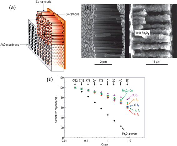 | ||
| Fig. 1 (a) Diagram of the nanostructured current collector expected to be obtained at the end of the electrolysis, before and after removal of the AAO membrane. (b) Cross-sectional views of Cu-nanostructured current collector before (left) and after (right) Fe3O4 deposits. (c) Rate capability plots for Fe3O4 deposits on Cu nanostructured electrodes. Adapted by permission from Macmillan Publishers Ltd: Nat. Mater., ref. 34 © 2006. | ||
Growth of 1D nanostructures on substrates via “high-temperature” process such as vapor–liquid–solid (VLS)/vapor–solid (VS) method and chemical vapor deposition (CVD) is another choice for preparing high-quality nanoarrays.53–55 For VLS growth, for example, small metal clusters consisting of noble metals (Au, Pt, etc.),56 are initially deposited on the surface of metal or semiconductor wafers. Placed in a reaction chamber or quartz tube, substrates are allowed to be heated in the temperature range of 300–1100 °C until metal clusters turn into liquid droplets.57 Then, a gas containing the precursor material is controlled and transported throughout the reaction tube. As the surface of the liquid droplet has a much larger sticking coefficient than the solid substrate, the precursor atoms prefer to deposit on the surface of the liquid and form an alloy; as a result, crystal growth occurs at the solid–liquid interface by precipitation, initiating the growth commences with 1D nanoarrays. In most cases, the size of liquid droplets eventually determines the diameter of 1D nanostructures. Typical examples are the fabrication of Si,58Ge or composite alloy nanorod/nanowire arrays for high-capacity LIBs. Generally, these materials that can alloy/dealloy with Li have long attracted a great deal of interest for negative electrodes of LIBs because of their dramatic capacities originating from multi-step electrochemical processes. Cui and his group reported for the first time that Ge nanowire array fabricated by using VLS growth on stainless steel substrate had good cycle performance when directly used as anode for LIBs.26Fig. 2a shows a single Ge nanowire with a diameter of ∼30 nm, revealing the typical characteristics of nanowire prepared by VLS mechanism; as obviously observed on the top of Ge nanowire, the nanosized Au particle acts as the catalyst, the size of which is quite comparable to that of Ge nanowire. The electrochemical cycling of Ge nanowire array remains stable after 20 cycles within a voltage window of 0.005∼2.5 V at the C/20 rate, and the specific capacity is maintained around 1000 mAh g−1 (Fig.2c).
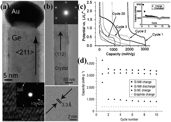 | ||
| Fig. 2 (a) TEM image and SAED pattern of Ge nanowire. HRTEM shows the 1/3(422) lattice fringes. Reprinted with permission from ref. 26. Copyright 2008 American Chemical Society. (b) TEM image and SAED spots of a single-crystalline, pristine Si nanowire. HRTEM lattice fringes (bottom) are from the Si 1/3(224) planes. (c) Constant current voltage profile at the C/20 rate for Ge nanowire arrays with the cycle life in the inset. (d) Capacity versus cycle number for the Si NWs from 2.0 to 0.01 V at the C/20 rate (20 h per half cycle) showing the charge (squares) and discharge capacity (circles). Adapted by permission from Macmillan Publishers Ltd: Nature Nanotechnology, ref. 61 © 2008. | ||
Up to date, silicon has been proposed as the most ideal candidate to replace conventional graphite electrode because of the large theoretical capacity up to 4200 mAh g−1 (Li21Si5).59 Nevertheless, the high capacity simultaneously brings about huge volume changes (∼300%) upon alloying with Li ions, leading to severe cracking and pulverization of electrode and furthermore capacity loss. Since oriented nanostructuring can lead to improvements in electrochemical reaction kinetics of electrode materials and thus the cycle and power performance of the batteries because of shortened ion diffusion distances and enhanced electron transport,60 some efforts have been made to realize various oriented forms of Si nanostructures. For the first time, Chan and Cui et al. successfully prepared an oriented single-crystalline Si nanowire array on a stainless steel substrate by using VLS method (gold serving as catalysts) (Fig. 2b).61 During the initial lithium insertion, Si nanowire array can be capable of charging up to the theoretical capacity in the absence of any obvious pulverization, as demonstrated in the work. After 10 cycles, Fig. 2d shows that 75% of the theoretical capacity can be maintained, without obvious capacity fade. Based on the concept that designing nanoscale hierarchical structures is a novel approach to address the issues associated with the large volume changes, Cui's group recently introduced a core-shell design of silicon nanowire arrays for high-power and long-life LIB electrodes62 The outstanding innovation is the sole employment of the shell of amorphous Si for Li storage while preserving the crystalline Si core as mechanical support and efficient electron transport pathway, realizing a high charge storage capacity (∼1000 mAh g−1, 3 times of carbon) with ∼90% capacity retention over 100 cycles. Also, excellent electrochemical performance at high rate charging and discharging (6.8 A g−1, ∼20 times of carbon at 1 h rate) was demonstrated. Series of proof-of-concept study revealed that building arrayed Si nanowires on current collectors could be promising for the development of advanced LIBs.
As reviewed, “high-temperature” method has provided a way of making some promising electrode nanomaterials through a high temperature chemical reaction process. As a result, requirements of technique itself endow the as-prepared materials with high qualities such as perfect crystalline structure, few defects and good conductivity. However, from the practical viewpoint, direct growth of electrode materials at high temperatures is not beneficial to the battery commercialization. There is a huge need to develop scalable and cost-effective (catalyst-free, low-temperature) techniques for the preparation of nanowire/nanorod/nanotube electrodes. On the other hand, the selection of other promising materials as anodes of LIBs such as metal oxides may to a large extent simplify the fabrication process.
Since solution growth methods can lower the required conditions for nanostructure synthesis, the ability to systematically manipulate the growth of various inorganic nanostructure arrays on substrates in the solution phase is an important goal in materials chemistry today.63–65 The main advantage of such solution-based methods could be the possibility to create arrays of nanostructures, especially the aforementioned metal oxide nanostructures on a large scale at low temperature (even at room temperature66) with low cost, and on various flexible substrates. The growth is governed by classical heterogeneous nucleation and subsequent crystal growth. In recent years, there have been an increasing number of reports on the solution growth of 1D oxide nanostructure arrays onto nonreactive conductive substrates and their straightforward application in LIBs, which will be intensively reviewed as the main content in the following sections.
3. Various 1D oxide nanostructure array electrodes
3.1 SnO2 nanorod/wire arrays
As an important n-type semiconductor, SnO2 has been regarded as a potential graphite substitute primarily owing to its high theoretical specific capacity (∼781 mAh g−1) and safety.67–70 More importantly, relatively low average working potential (<1.0 V) renders its superior practical value to other oxide anode materials. Thus, making 1D oriented nanostructure array of SnO2 on metal substrate over a large area and further applying it as anode of battery are not only significant to fundamental study but also highly desirable for the exploration of novel electrode materials. Wan et al. have once investigated the synthesis of massive SnO2 nanowires by the thermal evaporation method on button-type electrode for Li-ion batteries;71 whereas in the literature, it is worth mentioning that only a few reports have discussed the mass synthesis of well-oriented SnO2 nanorod/wire arrays,72–74 and almost all the reported SnO2 arrays were grown on glass and silicon wafers or within AAO templates, limiting their robust electrochemical applications. In addition, the dominant approach for growing well-ordered SnO2 nanoarrays on substrates relied on a technique based on the VLS mechanism. In this regard, precursor materials were heated up to a boiling point while non-stop transported and protected by inert gas flow at a relatively high temperature in a sealed atmosphere (quartz glass tube). Recently, Kim and his co-workers reported a direct growth of 1D SnO2 nanowires on the current collector (Si (100) or stainless steel foil) via a VLS method at 600 °C.75Fig. 3a,b show the low and magnified cross-sectional FESEM images of the SnO2 nanowires grown on the stainless steel foil, respectively, which reveal the straight and considerably long morphological features of the SnO2 nanowires as well as the sign of VLS mechanism: the presence of Au catalyst (Fig. 3c). Fig. 4a presents the collection of specific capacity versus cycle number plots for three different Sn-based electrodes. Each cell was cycled over the voltage window of 0.0∼1.2 V versusLi/Li+. In contrast to the SnO2 nanowire array electrode, the electrochemical performances of both the SnO2 and Sn nanopowder electrodes were drastically degraded, showing a rapid decrease in discharge/charge capacities with the increase of the cycle number. This remarkable difference in cycle stability is a clear evidence of the beneficial effects of the 1D nanostructures on the enhancement of cycling characteristics in Sn-based materials system. As emphasized in this work, an electrode of SnO2 nanowire array by a high-temperature growth process can deliver reversible discharge capacities of 600 mAh g−1 at 3C (2346 mA g−1), 530 mAh g−1 at 5C (3910 mA g−1), and 440 mAh g−1 at 10C (7820 mA g−1), meanwhile maintaining high coulombic efficiency of over 95% on average (Fig. 4b).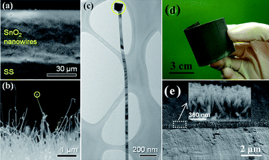 | ||
| Fig. 3 Typical (a) tilted and (b) magnified, cross-sectional FESEM images of the SnO2 nanowires. (c) TEM image of an individual SnO2 nanowire. Dashed circles in (b) and (c) indicate the nanowire tip, ref. 75. Copyright 2009 IOP. (d) Optical image and (e) Cross-sectional SEM images of the SnO2 nanorod array attained by hydrothermal method. Reprinted with permission from ref. 76. Copyright 2009 Royal Society of Chemistry. | ||
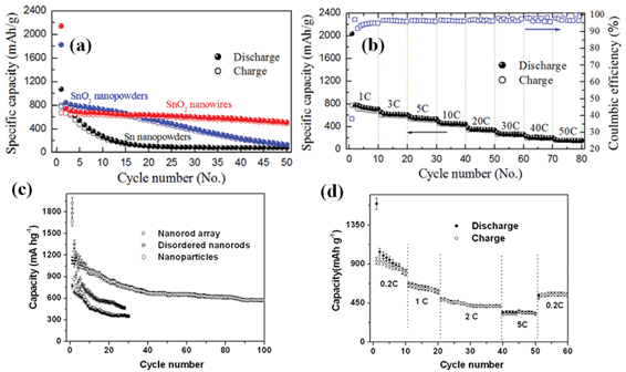 | ||
| Fig. 4 SnO2 nanoarray by VLS growth: (a) Specific capacity versus cycle number plots for three different Sn-based electrodes: SnO2 nanowires, SnO2 nanopowders, and Sn nanopowders. (b) Specific capacity versus cycle number of the SnO2 nanowire electrode cycled ten times at every C-rate (1 C, 3 C, 5 C, 10 C, 20 C, 30 C, 40 C, and 50 C) over 0.0–1.2 V and its corresponding Coulombic efficiency, ref. 75. Copyright 2009 IOP. Hydrothermally grown SnO2 nanoarray: (c) Cycling performance at the 0.1 C rate for the nanorod array, disordered nanorods, and nanoparticles(void: discharge; solid: charge). (d) Cycling performance at various C rates for nanorod array. Reprinted with permission from ref. 76. Copyright 2009 Royal Society of Chemistry. | ||
Generally, this method produced high aspect ratio SnO2 nanowires but has low productivity and high expenditure; that is, only a small quantity of product can be harvested, while usually coupled with the cost of noble metal (Au, Pt, etc.) as the catalyst and high temperature for the 1D growth. This is not encouraging to meet the demands when applied in practical use. As an alternative, low-temperature synthesis is more popular for the nanostructure array growth because of its facile manipulation on the morphology and the potential for large-scale and low-cost production.
In 2009, Liu et al. reported for the first time the synthesis of scalable well-oriented SnO2 nanorod/wire arrays on bulk alloy foil by employing a facile alkaline hydrothermal method, without any templates or catalysts.76 The key to synthesizing a self-ordered nanorod array of SnO2 on alloy was effectively slowing down the release of hydroxyl ions and water from Sn(OH)62−. Herein, it needs to be emphasized that alloy substrate is available for metallic current collector because it does not alloy with lithium while maintaining stable electrochemical properties even at a high voltage. Fig. 3d illustrates a typical photograph of SnO2 film uniformly grown on a ∼40 cm2 alloy substrate. In principle, considering the feasibility and generality of the hydrothermal method, it is reasonable that the growing area can be easily scaled up for practical applications by simply choosing a purpose-built apparatus. As is obvious from the optical image, the SnO2-covered substrate can be severely rolled without visible signs of degradation, indicating the flexibility and mechanical robustness of the as-prepared film; this feature implies possible application of the product in flexible electronics. Eventually, hydrothermally synthesized SnO2 nanoarray (Fig.3e) can exhibit good reliability, high capacity, long life-cycle and fast rate capability when tested as anode for LIBs in the range from 2.5 to 0.005 V. The discharge and charge capacity versus cycle number plots up to 100 cycles at 0.1C (78.1 mA g−1) for the array electrode is displayed in Fig. 4c and d. As seen, the capacity of ∼580 mAh g−1 can be retained after 100 cycles, 74.3% of the theoretical capacity of SnO2 and 1.56 times that of graphite. More importantly, the coulombic efficiency after the 10th cycle is always as high as 99%. Besides, the cell reveals good cyclability at 2 C (1562 mA g−1), or even at a rate as high as 5 C (3905 mA g−1). Upon decreasing the rate from 5C to 0.2C, ∼70% of the initial capacity at 0.2 C (156.2 mA g−1) can be recovered.
By controlling the concentration and molar ratio of the precursors (tin salt and NaOH), Liu et al. further demonstrated that the diameter, length, aspect ratio and growth density of SnO2 nanorods can be readily adjusted. The easy control of the array parameters is beneficial to studying the structure–property relationship and thus makes it possible to fine-tune the electrochemical performance. Their comparative studies revealed that, in general, to obtain a good electrochemical property, the as-grown nanorods should have a small diameter and relatively low growth density, which would allow only a limited volume change and reduced lithium diffusion length, as well as fast electrolyte diffusion and good strain accommodation.
3.2 ZnO-based nanowire arrays
ZnO, as a versatile functional material, is a well-known Li insertion compound but was investigated only during the early years of Li battery research.77 Normally, ZnO itself has been demonstrated to be not a good electrode material when used as anode for LIBs, although its discharge capacity is up to ∼987 mAh g−1 in theory. Bulk ZnO generally suffers from poor kinetics and severe capacity fading upon cycling, even at low rates.78 This is because Zn nanograins generated from the replacement reaction between ZnO and Li migrate through the Li2O matrices faster than other metal nanoparticles such as Sn upon the volume variation and therefore aggregate much faster. For 1D/2D well-aligned nanoarrays of ZnO and various ZnO nanostructure powders, even though the reduced size could somewhat limit the volume change and the Zn aggregation, the loss of electrical contact arising from the volume expansion-contraction during the charge-discharge process is still a serious problem. As an alternative concept, in situ incorporation of homogeneous ZnAl2O4 buffer (inactive material) into ordered ZnO nanosheets (active materials) at nanoscale (<10 nm) via the calcination of layered double hydroxide precursor has been reported and highlighted as a functional way to improve the reversible capacity and upgrade the lifetime, but relatively poor electronic conductivity of ZnO/ZnAl2O4 still limits the rate capability.79 In principle, how to achieve better rate performance and longer lifespan of ZnO-based LIBs while maintaining high capacity has become a great challenge that needs to be addressed.Creating nanostructures that comprise Li alloying phase such as Sn uniformly dispersed in carbon phase or that was homogeneously coated by carbon shell is an attractive approach to mitigate the mechanical strain/stress and enhance the electronic conductivity, thereby improving the cycle life and rate capability.8 Enlightened by this, coating highly crystalline ZnO nanostructure array with conductive carbon would be an effective means of improving the electrochemical property at high current rates. However, it is not easy to extend this good concept to metal oxides, especially to arrays of metal oxide nanostructures. The penetration of carbon-containing precursor into the arrays is not as easy as that for powders; in addition, the preparation of conductive carbon (at least partially graphitized) normally needs a high temperature treatment, which makes the fabrication of oxides/carbon nanocomposite structure troublesome because of the possible unavoidable redox reaction between oxides and carbon and even the presence of Kirkendall effect.80 Recently, Ding and her co-workers synthesized a carbon-based micro-tubular structure from a carbonaceous species-coated ZnO nanorod on the basis of the nanoscale Kirkendall effect and in situZn evaporation at 900 °C, clearly demonstrating the inaccessibility of forming a complete carbon/oxide composite phase at high temperature.81 When the annealing temperature is low, the composite structure can be maintained but such amorphous carbonaceous species would severely affect the capability of electron transport and in turn deteriorate battery performance. Thus, finding a reasonable annealing temperature becomes crucial to determine the electrochemical properties of carbon/metal oxide electrode materials. Very recently, Liu et al. successfully fabricated carbon/ZnO nanowire arrays on nickel substrate over a large area by the simple carbonization of preadsorbed glucose on ZnO arrays at 500 °C in argon gas,82a the morphology of which is displayed in Fig. 5a. The carbon content is ∼3.0 wt %. Inset in Fig. 5a is an optical image of 14 mm sized carbon/ZnO array electrode (black). Fig. 5b depicts the Raman spectrum of the array (excitation wavelength: 532 nm), which shows two obvious peaks located at 1340 (D-band) and 1588 cm−1(G-band), confirming the presence and partial graphitization of carbon. The decoration of carbon on the surface of single-crystalline ZnO nanowire is evidenced by the high-resolution TEM (HRTEM). As shown in Fig. 5c, a uniform coating of average 6 nm carbon shell on ZnO nanowire surface is demonstrated. Substantially improved cycling performance has been observed, as in Fig. 6a. The inset is the SEM image of carbon/ZnO array after cycling at 0.75 C (740.85 mA g−1) for 50 times. Particularly, the most important is revealed that carbon/ZnO electrode can preserve the array configuration and conductivity; the presence of carbon shell on the nanowire surface would effectively alleviate the strains caused by the volume variation of ZnO nanowire cores and prevent the disintegration. Meanwhile, carbon itself is a good electronic conductor. With the full and uniform coating of carbon, electrons can easily reach all the positions where Li+ ion intercalation takes place.
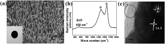 | ||
| Fig. 5 (a) SEM image of carbon/ZnO nanorod arrays. Inset is an optical image of the electrode. (b) Raman spectrum of the arrays. Excitation laser wavelength: 532 nm. (c) HRTEM image and SAED pattern of an individual carbon/ZnO nanorod. The circle indicates the presence of carbon shell. Reprinted with permission from ref. 82a. Copyright 2009 American Chemical Society. | ||
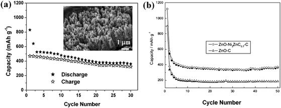 | ||
| Fig. 6 (a) Cycling stability of carbon/ZnO array at 0.75 C. Inset shows the SEM image of carbon/ZnO array after cycled at 0.75 C for 50 times. Reprinted with permission from ref. 82a. Copyright 2009 American Chemical Society. (b) Cycling stability of ZnO–Ni3ZnC0.7–C and ZnO–C electrodes at a current density of 0.2 mA cm−2 (solid symbols: charge; hollow symbols: discharge) ref. 84. Copyright 2010, The Electrochemical Society. | ||
This is the first example of coating metal oxide nanostructure array electrode with carbon nanomaterials, with the combination of the good electroactivity of carbon and electrochemical advantages of ordered array architecture. It should be further pointed out that the ZnO nanowire arrays became porous after many times cycling due to repeated Li+ insertion/extraction and the volume expansion in this process, as shown in the inset of Fig. 6a. This common process, when controlled carefully, was recently utilized by Cui et al.82b to generate purpose-designed and well-defined porous nanowire arrays, which may hold great promise in future photoelectronic devices.
Since the catalytic function of metallic nickel was found to facilitate the decomposition of Li2O (Li2O + Ni → NiO + 2Li+ + 2e−) during the charge process and improve the reversible capability of ZnO,83 making a Ni-based composite structure becomes interesting for developing better batteries. Lately, Pan and his co-workers have successfully prepared a core-shell ZnO–Ni3ZnC0.7–C composite84 (in which carbon content is 24.1 wt %) by the pyrolysis of Zn/Ni-based organic precursors and confirmed that lithium storage capacity of this composite anode was significantly enhanced by Ni3ZnC0.7 incorporation, much better than that of C/ZnO powder, as obviously demonstrated in Fig. 6b. Ni3ZnC0.7 phase was believed to act as catalyst for the Li2O decomposition as well as good electronic conductor. This novel mechanism may somehow shed new light on the development of advanced LIBs. However, the concept of using C/Ni-based composite as anode was studied with the focus on the mixed powders of nanoparticles rather than aligned nanoarray structure. To further improve battery performance, systematic investigation of coating both carbon and catalytic metal on well-designed nanostructure arrays is highly necessary in a future study, as this will further integrate the merits of ordered arrays into the electrode materials system.
3.3 CoOx nanowire arrays
Since the discovery of reversible conversion mechanism of lithium storage by Tarascon et al. in 2000,12cobalt-based oxides (CoOx), including cobalt oxide (Co3O4) and cobalt monoxide (CoO), have stimulated a great enthusiasm in the field of energy storage. By possessing a superior specific capacity (896 mAh g−1 in theory) and good capacity retention ability,85,86Co3O4 has been reported to be a promising alternative anode material for the next generation of LIBs. Therefore, to give a full scope to the electrochemical capability of this material, the realization of 1D nanostructure array of Co3O4 is highly expected by engineers and scientists. At the early stage, traditional template synthesis was studied to prepare 1D nanostructures of Co3O4 by employing porous membranes (AAM), surfactants (soft template) or even virus.87 In view of the drawbacks of using these templates as reviewed in Section 2, fabricating 1D nanostructures of high-purity Co3O4 without any assisted templates remained challenging in the early years. Later, although some methods for the direct synthesis of Co3O4 nanostructures was developed by the decomposition of cobalt-based carbonate precursor,88 the lack of general synthesis of Co3O4 with well-arrayed architecture on conductive substrate still needed to be addressed.In 2008, Wu and co-workers reported for the first time the successful growth of self-supported mesoporous Co3O4 nanowire array (NWs) on various substrates, such as Si wafer, glass slide, Cu or Ti foil, and even conductive plastic substrates.36,89 In addition, Co3O4 NWs are almost single-crystalline and mesoporous resulting from the topotactic transformation from Co(OH)2 during the later growth process. The synthesis was based on an ammonia-evaporation-induced process, in which the nanowires were derived from the hydrolysis of cobalt-ammonia complex ions. Fig. 7a–c show typical cross-sectional view and top-view SEM images of mesoporous Co3O4 NWs. With a high initial coulomic efficiency of ∼76% at a current rate of 111 mA g−1, the NW arrays maintain stable capacity at 700 mAh g−1 after 20 cycles, which is so much better than that of non-self-supported NWs (350 mAh g−1) and commercial powders (80 mAh g−1) (Fig. 7d). Accompanied with capacity retention tests, in-depth morphological and intrinsic characterizations towards recharged NWs electrode were also conducted, demonstrating that NW arrays can survive tens of cycles with only slight deformation. Moreover, this work also got insight into the compositional and structural changes of Co3O4 NWs at different stages of the electrochemical reaction, with the aim of having a clear understanding of capacity loss by XRD analysis of as-prepared sample (bottom), discharged sample (middle), and recharged sample (top) (Fig. 7e). When the cell was completely discharged, the diffraction peaks of Co3O4 disappeared but a peak at 32.6° and a broad weak peak at 44.2° appeared instead, assigned to Li2O (111) and Co (111), respectively. This is consistent with the conversion reaction mechanism in which Co3O4 is reduced, forming metallic Co nanodomains embedded in the Li2O matrix. However, when charging the cell back to 3.0 V, it is interesting to find that no Co3O4 peaks reappeared when the broad and weak Co peak vanished in the XRD pattern. Instead, a weak peak at 34.2° appeared that can be assigned to β-CoO (111) planes, which indicates that β-CoO is the recovered species after the first full electrochemical cycle. Wu's work not only presented a means to improve the battery performance of Co3O4 anode, but also provided a clear view of the electrochemical lithium storage kinetics and mechanism of ordered nanostructure array.
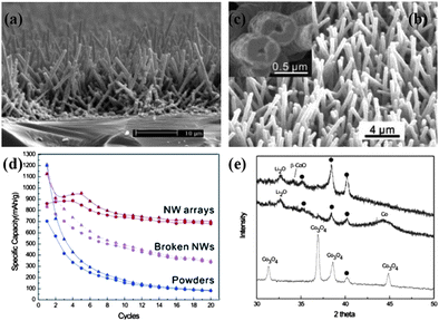 | ||
| Fig. 7 (a–c) Typical SEM images of Co3O4 nanowire arrays. Reprinted with permission from ref. 89. Copyright 2006 American Chemical Society. (d) Specific capacity of the Co3O4 NW array on Ti foil (red), non-self-supported NWs (magenta), and commercial powders (blue) as a function of the cycle number. (e) XRD patterns of as-prepared sample (bottom), discharged sample (middle), and recharged sample (top). Reprinted with permission from ref. 36. Copyright 2008 American Chemical Society. | ||
Cobalt monoxide (CoO), as another possible anode material for LIBs owing to its completely reversible electrochemical reaction and relatively high theoretical capacity of ∼716 mAh g−1, has been investigated as well.90 Whereas accessible cost-effective synthesis of high-quality CoO with well-designed nanostructures has seldom been attained during the past decade because of limitations arising from traditional preparation methods (sol–gel, electrochemical method, etc.), let alone the fabrication of CoO 1D nanostructure array.91,92 Thanks to the successful realization of large-scale arrays of 1D nanostructured cobalt-hydroxide-carbonate on various substrates (including metal substrates, glass slide, and even ceramic),93 the template-free preparation of a nanoarray of low-dimensional CoO has become possible. Jiang et al. recently reported a facile and direct synthesis of large-scale CoO porous nanowire array with robust mechanical adhesion to flexible conductive substrate (Ti foil) by the complete pyrolysis of cobalt-hydroxide-carbonate.94Fig. 8a shows the representative SEM image of CoO nanowire array on Ti substrate, and the inset reveals that each nanowire has a sharp tip. From TEM image (Fig. 8b,c), the diameter of single nanowire is of ∼100 nm on average, which is smaller than that of aforementioned mesoporous Co3O4 nanowire. Obviously, large quantities of pores exist in the CoO nanowires, the yield of which can be attributed to the decomposition of hydroxide-carbonate and the release of gases (CO2, H2O) during the calcination process. In comparison to the traditional preparations, the whole process was dominated easily and no extra impurities were introduced. Meanwhile, the work also presented a smart way of synthesizing low-valence transition metal oxides by thermal decomposition of the corresponding carbonate precursors in an inert atmosphere.
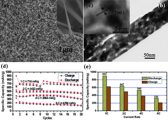 | ||
| Fig. 8 (a) SEM image, (b) TEM image, and (c) HRTEM image of large-scale uniform CoO NWAs on Ti substrate. (d) Rate and cycling performances and (e) Initial charge/discharge capacities of CoO NWAs at 1 C, 2C, 4 C, 6C respectively. Reprinted with permission from ref. 94. Copyright 2010 American Chemical Society. | ||
Encouraged by the general interest in high-power energy storage, the electrochemical investigations have been mainly emphasized on the rate capability of CoO NWAs (Fig. 8d and e). In detail, tests with high rates of 1C (716 mA g−1), 2C (1432 mA g−1), 4C (2846 mA g−1) and 6C (4296 mA g−1) from 3.0 to 0.005 V have been conducted, respectively. After 20 cycles, it could be observed that capacities of 670 mAh g−1 (1C), 464 mAh g−1 (2C), 312 mAh g−1 (4C), 150 mAh g−1 (6C) can still be maintained. As the charge-discharge rate increases from 1C to 6C, it is important to find the initial coulombic efficiency is still maintained to 70% on average, without an immediate decrease. It is considered that the good rate performance could be potentially associated with not only the robust electrochemical contact between electrode current collector and active materials, but also the designed morphology.95 The establishment of 1D architecture can benefit the fast transport of electrons along the same direction, substantially shortening the pathway. Meanwhile, the existence of pores in nanowires plays an important role: porous structures are able to facilitate rapid ionic motion and accommodate the strain induced by the volume change, finally enhancing the comprehensive performance of electrode.
3.4 Fe2O3-based nanotube arrays
The interest in the study of iron oxides including hematite (α-Fe2O3), magnetite (Fe3O4) and ferrous oxide (FeO) stems from their potential in both biological and industrial applications. Environmentally benign material of α-Fe2O3, the most stable phase of iron oxides and widely existing resource on earth, has a broad technological potential in gas sensors, catalysis, field emission, magnetic storage, and pigments.96–98 Particularly, it is also a promising anode material (theoretical capacity: 1007 mAh g−1) for LIBs.99 With respect to preparing arrayed forms of 1D Fe2O3 on conductive substrates, typical synthesis methods are all limited to traditional templating approaches in combination with some assisted technologies such as electrochemical anodization, atomic layer deposition (ALD) and so on.100 Among various geometric types of objects, tubes offer an additional degree of freedom in their design as compared to wires, in that not only the length and diameter can be varied but also the thickness. Before long, Bachmann et al. reported on the fabrication of iron oxide nanotubes by ALD and the opportunities thus afforded in the magnetic realm.101 In their report, porous anodic alumina membranes must be prepared at first according to a two-step electrochemical method and then an ALD deposition of smooth Fe2O3 layer was carried out (Fig. 9a), yielding arrays of tubes with aspect ratios up to 100. The proposed method can realize the arrays of smooth α-Fe2O3 tubes with a geometry (wall thickness, external diameter, etc.) that is readily controlled and widely tunable, but many restricted factors arising from template and technology such as complicated template removal make it not achieve leapfrog technological progress. One of recent achievements in fabrication of Fe2O3 nanotube arrays is the development of a new formation mechanism called “sacrificial template-accelerated hydrolysis” (STAH).102 Typically, this new concept involves acid-dissoluble metal oxide template and easily-hydrolyzed metal salt precursor; the possibility of selecting appropriate pairs of template and precursor renders this concept with tremendous flexibility and makes it potentially extendable to a wide variety of nanotube materials. Fig. 9b illustrates schematically the synthetic strategy for the design of iron oxide nanotube arrays. Herein, ZnO nanostructure arrays are judiciously used as the starting template due to their low cost, easy fabrication and abundant available morphologies. Progressive hydrolysis of Fe3+ and template dissolution by the acid from hydrolysis can promote each other and eventually result in well-oriented Fe(OH)3 nanotube arrays. Annealing the Fe(OH)3 arrays in different atmospheres leads to different iron oxides, in which α-Fe2O3 nanotube array is obtained by annealing in Ar gas. Compared with previous reactive templates, the ZnO template does not contribute to the component of final nanotubes, but can be in situ dissolved automatically; post-treatment for template removal is not necessary.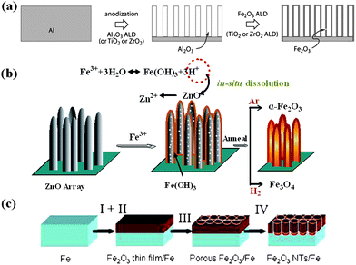 | ||
| Fig. 9 Schematic diagrams of the formation process of iron oxide nanotube arrays by (a) traditional AAO templating method. Reprinted with permission from ref. 101. Copyright 2007 American Chemical Society. (b) STAH method. Reprinted with permission from ref. 102. Copyright 2010 American Chemical Society. (c) sonoelectrochemical anodization method. Reprinted with permission from ref. 103. Copyright 2009 American Chemical Society. | ||
Electrochemical anodization method is also an effective way of making tubular nanostructures of various metal oxides on conductive substrates. Lately, Misra et al. developed a simple sonoelectrochemical anodization method to grow smooth and ultrathin (5–7 nm thick) Fe2O3 nanotube arrays (3–4 μm long) on Fe foil with only 13 min reaction.103 The growth mechanism is illustrated in Fig. 9c. Firstly, Fe oxidizes to form a thin layer of Fe2O3 on metal at the solid-liquid interface. Hereafter, the presence of a complexing ligand and high applied potential gives rise to substantial dissolution of Fe2O3, forming a self-standing individual nanotube structure on Fe foil, which is quite identical to the preparation of TiO2 nanotubes under similar chemical conditions.104,105 Although the total synthesis of Fe2O3 nanotube arrays is completely free from templates, the formation process requires more conditions than template-based approaches; complex electrochemical system is essential for initial corrosions on the surface of metals, and the further breakage of corrosion layer needs a high potential to yield ordered nanoporous structure in the case of a homogeneous chemical dissolution, and should be assisted by continuous ultrasonic waves.
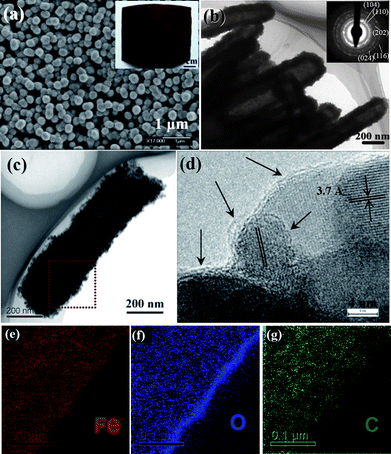
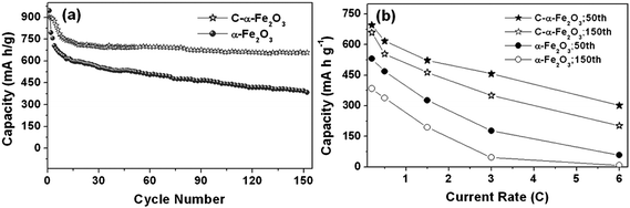
With regard to the battery performance, we focus on reviewing the electrochemical behavior of α-Fe2O3-based nanotube arrays made by “STAH” mechanism. Fig. 10a and b display SEM/TEM images of α-Fe2O3 nanotube arrays and indicate that columnar nanotubes have closed tips and are assembled from numerous nanoparticles. This is quite understandable and consistent with the growing process of “STAH”; the progressive hydrolysis of Fe3+ and dissolution of ZnO at room temperature lead to a simple accumulation of Fe(OH)3 nanoparticles rather than anisotropic crystal growth. The inset image in Fig. 10a reveals the growth area on alloy can be as large as ∼30 cm2. Fig. 10c shows the TEM micrograph of an individual C/α-Fe2O3 nanotube of ∼200 nm diameter derived from STAH. The homogeneous existence of Fe, O, and carbon in the nanotube wall is unambiguously illustrated in Fig. 10e–g by EELS elemental mapping. The carbon content is determined to be ∼10.7% by thermogravimetric analysis (TGA). This result confirms that a carbon source can be successfully introduced with a facile addition of glucose into the Fe3+ precursor solution. Indicated by arrows in Fig.10d, thin carbon layers of average 1.5 nm in thickness are coated tightly on the surface of most α-Fe2O3 nanoparticles. The uniform carbon coating benefits from the homogeneous adsorption of glucose onto the surface of Fe(OH)3 nanoparticles, revealing the novelty of STAH method for nanoscale carbon painting. Fig. 11a shows the distinct difference between C/α-Fe2O3 and α-Fe2O3 nanotube array electrodes in the cycling performance up to 150 cycles at C/5 (1C = 671 mA g−1). After 150 cycles, the C/α-Fe2O3 electrode still delivers a reversible capacity of as high as 659 mAh g−1 in the potential range of 0.005∼3 V, with a fading rate of only ∼0.586 mAh g−1 per cycle during the last 70 cycles, while for the pristine α-Fe2O3 electrode, the capacity decreases continuously and only 384 mAh g−1 can be retained at the end. Considering that no traditional carbon black and polymer binders were used, the enhanced lifecycle of C/α-Fe2O3 nanotube arrays is mainly attributed to the introduced nanosized carbon and the tubular structure. Evidently, C/α-Fe2O3 nanotubes comprise numerous nanoparticle subunits, which are α-Fe2O3 particles encapsulated within thin carbon shells. Every shell is tightly attached to α-Fe2O3, favorable for mechanical reinforcement and electrical conductivity enhancement. At a size scale smaller than 20 nm, the volume change of α-Fe2O3 upon Li uptake and removal can be minimized more efficiently by the mechanical buffering of the carbon shell. Meanwhile, the carbon coating around every α-Fe2O3 nanoparticle also ensures an electrical contact throughout the whole nanotube body during the cycling. Further, the hollow space of nanotubes offers better electrolyte accessibility and can accommodate a larger degree of structural deformation due to volume variation during Li insertion/extraction.
 | ||
| Fig. 10 (a) Low-magnification and (b–c) TEM images and SAED pattern of several α-Fe2O3 nanotubes. Inset is a typical optical image of the array on a large-area alloy substrate. (d) HRTEM image of the C/α-Fe2O3 nanotube. Arrows indicate the carbon layers. (e–g) EELS elemental mapping results. Reprinted with permission from ref. 102. Copyright 2010 American Chemical Society. | ||
 | ||
| Fig. 11 (a) Cycling performance at the C/5 rate (134.2 mA g−1) for α-Fe2O3 and C/α-Fe2O3 nanotube arrays from 3.0 to 0.005 V. (b) The charge capacity versus current rate plots of α-Fe2O3 and C/α-Fe2O3 nanotube arrays. Reprinted with permission from ref. 102. Copyright 2010 American Chemical Society. | ||
The C/α-Fe2O3 nanotube array electrode shows a long cycle life while still exhibiting a relatively high capacity even at high current rates, as illustrated in Fig.11b. The reported carbon decoration processing is quite different from the literature that carbon was typically coated on the outline of the overall nanostructures or used for nanostructures loading. Actually, we could comprehend the oriented conducting superhighways are constructed by numerous building blocks consisting of thin carbon-layer-coated α-Fe2O3 nanoparticles rather than pure α-Fe2O3 nanotubes simply shelled with a carbon layer outside. Another noticeable structural feature of the C/α-Fe2O3 nanotubes is that there are abundant mesopores in the tube walls. The porous nature allows a fast Li-ion diffusion and provides larger material-electrolyte contact areas, rendering an increased number of electrochemically active surface sites. Thus, the reported C/α-Fe2O3 electrode material bring the porosity, hollow cavity, electronic conductivity, and ordered array structure together, making it very promising for high-energy and high-power energy storage. It also sheds light on the development of other transition metal oxide-based composite porous nanotube array electrodes.
We noticed that the nanocarbon distributed in the nanotube walls was still poorly graphitized since the annealing temperature was lower than 500 °C. However, raising the temperature to improve the graphitization degree (electrical conductance) of carbon is not reasonable considering that carbon can easily react with multivalent metal oxides (such as react with α-Fe2O3 to produce Fe3O4). This will lead to difficulty in precisely controlling the composite components although the generated Fe3O4 is more conductive than α-Fe2O3 and can be used as anode for LIBs.106 The relatively poor conductivity of nanocarbon in carbon-metal oxide composites as compared with graphite makes it impossible to further optimization of the electrochemical performance, which needs to be addressed in future study.
For the above discussed metal oxide array electrodes, the improvement of their electrochemical performance was researched recently107–109via other routes such as growing 1D belt-like or hollow nanostructures; this should also attract our attention.
4. Concluding remarks
Building advanced materials for electrochemical energy storage is a complex challenge that has been taken on by many researchers. For LIBs, finding potential anode materials with high capacity, long lifespan and good power performance to replace the commercially used graphite has long been considered a big issue and has triggered tremendous fundamental studies. While encouraging progress has been achieved in this field, the use of 1D nanostructure arrays as anodes attracted researchers' attention only in recent years. All the typical examples of using ordered metal oxide arrays grown directly on conductive metal substrates for LIBs anodes have been reviewed herein. However, after several years of intensive research with tens of publications in the literature, the current electrochemical performance of metal oxides does not support a direct rapid technical application in the near future. There is still a huge space to exploit by growing other potential metal oxide nanostructure array electrodes for LIBs.The major problem with most metal oxide anodes is the relativity poor lifecycle as compared to graphite, which partially results from the medium conductivity and nonlayered crystal structure. As discussed above, growth of metal oxide onto conductive substrates (that can be employed directly as current collectors) has shown some potential in improving the transport pathway of electrons, but the introduction of additives such as nanocarbon is still highly necessary. Further effort is required for increasing the conductivity of nanocarbon incorporated into oxide nanostructure arrays and designing carbon-metal oxide arrays with hierarchical carbon hybridization at both nanoscale (<10 nm) and submicroscale (several hundred nanometres). This may need to explore novel fabrication techniques by referring to knowledge of physics, chemistry and materials science. Alternatively, replacing nanocarbon with nanosized metals to make composite nanostructure arrays with metal oxides is another choice in the future. On the other hand, creating meso and macro-pores in oxide nanostructure arrays can to some extent compensate for the huge volume expansion and structural deformation derived from lithium insertion and take-up into/from nonlayered crystal structure. The effects of pore size, uniformity and distribution on the electrochemical lithium storage as well as the related electrochemical dynamics and pore wall/electrolyte interface interaction have to be intensively exploited.
As is well known, the current LIB system is not only limited by the performance of the anode. The concept reviewed herein that using ordered arrays directly grown on current collectors to promote the transport pathways of electrons and ions as well as to enhance the electrochemical reaction kinetics can definitely be applied to cathode materials. It is possible to expect a breakthrough improvement of the cycle life and rate performance of LIBs if electrode material developments can be systematically investigated along the already developed avenues in combination with the progress made in electrolyte and membrane.
Acknowledgements
Financially supported by self-determined research funds of CCNU from the colleges' basic research and operation of MOE (No.CCNU09A01019), the National Natural Science Foundation of China (No. 50872039), China Postdoctoral Science Foundation (20090460996), the Open Project Program of Key Laboratory of Quak & Lepton Physics (Huazhong Normal University), Ministry of Education, China (QLPL200902).References
- M. Armand and J.-M. Tarascon, Nature, 2008, 451, 652 CrossRef CAS.
- K. Kang, Y. S. Meng, J. Berger, C. P. Grey and G. Ceder, Science, 2006, 311, 977 CrossRef CAS.
- (a) Y. Wang and G. Z. Cao, Adv. Mater., 2008, 9999, 1; (b) J. Liu, G. Z. Cao, Z. G. Yang, D. H. Wang, D. Dubois, X. D. Zhou, G. L. Graff, L. R. Pederson and J. G. Zhang, ChemSusChem, 2008, 1, 676 CrossRef CAS; (c) J. Chen and F. Y. Cheng, Acc. Chem. Res., 2009, 42, 713 CrossRef CAS; (d) Y. G. Guo, J. S. Hu and L. J. Wan, Adv. Mater., 2008, 20, 2878 CrossRef CAS.
- J. Hassoun, P. Reale and B. Scrosati, J. Mater. Chem., 2007, 17, 3668 RSC.
- P. G. Bruce, B. Scrosati and J.-M. Tarascon, Angew. Chem., Int. Ed., 2008, 47, 2930 CrossRef CAS.
- A. S. Arico, P. G. Bruce, B. Scrosati, J. M. Tarascon and W. V. Schalkwijk, Nat. Mater., 2005, 4, 366 CrossRef CAS.
- M. Green, E. Fielder, B. Scrosati, M. Wachtler and J. S. Moreno, Electrochem. Solid-State Lett., 2003, 6, A75 CrossRef CAS.
- (a) G. Derrien, J. Hassoun, S. Panero and B. Scrosati, Adv. Mater., 2007, 19, 2336 CrossRef CAS; (b) Y. S. Hu, R. D. Cakan, M.-M. Titirici, J.-O. Müller, R. Schlögl, M. Antonietti and J. Maier, Angew. Chem., Int. Ed., 2008, 47, 1645 CrossRef CAS.
- G. L. Cui, L. Gu, L. J. Zhi, N. Kaskhedikar, P. A. Aken, K. Mullen and J. Maier, Adv. Mater., 2008, 20, 3079 CrossRef CAS.
- H.-L. Zhang, F. Li, C. Liu and H.-M. Cheng, Nanotechnology, 2008, 19, 165606 CrossRef.
- Y. Idota, T. Kubota, A. Matsufuji, Y. Maekawa and T. Miyasaka, Science, 1997, 276, 1395 CrossRef CAS.
- P. Poizot, S. Laruelle, S. Grugeon, L. Dupont and J. M. Tarascon, Nature, 2000, 407, 496 CrossRef CAS.
- B. Varghese, M. V. Reddy, Y. W. Zhu, C. S. Lit, T. C. Hoong, G. V. S. Rao, B. V. R. Chowdari, A. T. S. Wee, C. T. Lim and C. H. Sow, Chem. Mater., 2008, 20, 3360 CrossRef CAS.
- J. Chen, L. N. Xu, W. Y. Wang and X. W. Lou, Adv. Mater., 2005, 17, 582 CrossRef CAS.
- K. M. Shaju, F. Jiao, A. Debart and P. G. Bruce, Phys. Chem. Chem. Phys., 2007, 9, 1837 RSC.
- H. Li, Z. X. Wang, L. Q. Chen and X. J. Huang, Adv. Mater., 2009, 21, 1.
- T. Muraliganth, A. V. Murugan and A. Manthiram, Chem. Commun., 2009, 7360 RSC.
- S. Mitra, P. Poizot, A. Finke and J. M. Tarascon, Adv. Funct. Mater., 2006, 16, 2281 CrossRef CAS.
- D. Aurbach, M. D. Levi, E. Levi and A. Schechter, J. Phys. Chem. B, 1997, 101, 2195 CrossRef CAS.
- M. G. Kim and J. Cho, Adv. Funct. Mater., 2009, 19, 1.
- Z. H. Wen, Q. Wang, Q. Zhang and J. H. Li, Adv. Funct. Mater., 2007, 17, 2772 CrossRef CAS.
- Y. Wang, F. Su, J. Y. Lee and X. S. Zhao, Chem. Mater., 2006, 18, 1347 CrossRef CAS.
- S. H. Ng, D. I. dos Santos, S. Y. Chew, D. Wexler, J. Wang, S. X. Dou and H. K. Liu, Electrochem. Commun., 2007, 9, 915 CrossRef CAS.
- L. W. Ji and X. W. Zhang, Electrochem. Commun., 2009, 11, 1146 CrossRef CAS.
- C. C. Hu, K. H. Chang, M. C. Lin and Y. T. Wu, Nano Lett., 2006, 6, 2690 CrossRef CAS.
- C. K. Chan, X. F. Zhang and Y. Cui, Nano Lett., 2008, 8, 307 CrossRef CAS.
- Z. G. Wu, J. B. Neaton and J. C. Grossman, Phys. Rev. Lett., 2008, 100, 246804 CrossRef.
- B. Varghese, Y. S. Zhang, L. Dai, V. B. C. Tan, C. T. Lim and C.-H. Sow, Nano Lett., 2008, 8, 3226 CrossRef CAS.
- C. C. Li, Z. F. Du, L. M. Li, H. C. Yu, Q. Wan and T. H. Wang, Appl. Phys. Lett., 2007, 91, 032101 CrossRef.
- J. Elias, T.-Z. Ramon, G. Y. S. Wang and L.-C. Claude, Chem. Mater., 2008, 20, 6633 CrossRef CAS.
- W. Z. Wang, B. Q. Zeng, J. Yang, B. Poudel, J. Y. Huang, M. J. Naughton and Z. F. Ren, Adv. Mater., 2006, 18, 3275 CrossRef CAS.
- Z. L. Wang and J. H. Song, Science, 2006, 312, 242 CrossRef CAS.
- J. Bisquert, Phys. Rev. Lett., 2003, 91, 010602 CrossRef.
- P. L. Taberna, S. Mitra, P. Poizot, P. Simon and J.-M. Tarascon, Nat. Mater., 2006, 5, 567 CrossRef CAS.
- J. R. Jennings, A. Ghicov, S. P. Albu and P. Schmuki, J. Am. Chem. Soc., 2008, 130, 13364 CrossRef CAS.
- Y. G. Li, B. Tan and Y. Y. Wu, Nano Lett., 2008, 8, 265 CrossRef CAS.
- H. J. Fan, P. Werner and M. Zacharias, Small, 2006, 2, 700 CrossRef CAS.
- Y. Lin, T. Xie, B. C. Cheng, B. Geng and L. Zhang, Chem. Phys. Lett., 2003, 380, 521 CrossRef CAS.
- C. R. Martin, Science, 1994, 266, 1961 CrossRef CAS.
- D. J. Lipomi, R. C. Chiechi, M. D. Dickey and G. M. Whitesides, Nano Lett., 2008, 8, 2100 CrossRef CAS.
- C. H. Kim, H. J. Chun, D. S. Kim, S. Y. Kim and J. Park, Appl. Phys. Lett., 2006, 89, 223103 CrossRef.
- L. Liao, B. Yan, Y. F. Hao, G. Z. Xing, J. P. Liu, B. C. Zhao, Z. X. Shen, T. Wu, L. Wang, J. T. L. Tong, C. M. Li, W. Huang and T. Yu, Appl. Phys. Lett., 2009, 94, 113106 CrossRef.
- W. Xiao, D. L. Wang and X. W. Lou, J. Phys. Chem. C, 2010, 114, 1694 CrossRef CAS.
- J. P. Liu, X. T. Huang, Y. Y. Li, X. X. Ji, Z. K. Li, X. He and F. L. Sun, J. Phys. Chem. C, 2007, 111, 4990 CrossRef CAS.
- W. J. Dong, T. R. Zhang, J. Epstein, L. Cooney, H. Wang, Y. B. Li, Y. B. Jiang, A. Cogbill, V. Varadan and Z. R. Tian, Chem. Mater., 2007, 19, 4454 CrossRef CAS.
- G. Che, K. B. Jirage, E. R. Fisher and C. R. Martin, J. Electrochem. Soc., 1997, 144, 4296 CAS.
- C. L. Yan and D. F. Xue, Adv. Mater., 2008, 20, 1055 CrossRef CAS.
- F. Y. Cheng, Z. L. Tao, J. Liang and J. Chen, Chem. Mater., 2008, 20, 667 CrossRef CAS.
- C. R. Martin, Chem. Mater., 1996, 8, 1739 CrossRef CAS.
- S. Shingubara, O. Okino, Y. Sayama, H. Sakaue and T. Takahagi, Solid-State Electron., 1999, 43, 1143 CrossRef CAS.
- W. Wang, Y. Liu, C. Xu, C. Zheng and G. Wang, Chem. Phys. Lett., 2002, 362, 119 CrossRef CAS.
- R. C. Furneaux, W. R. Rigby and A. P. Davidson, Nature, 1989, 337, 147 CrossRef CAS.
- G. Z. Shen, P. C. Chen, K. M. Ryu and C. W. Zhou, J. Mater. Chem., 2009, 19, 828 RSC.
- X. H. Han, G. Z. Wang, L. Zhou and J. G. Hou, Chem. Commun., 2006, 212 RSC.
- Z. W. Pan, Z. R. Dai and Z. L. Wang, Science, 2001, 291, 1947 CrossRef CAS.
- K. Haraguchi, T. Katsuyama, K. Hiruma and K. Ogawa, Appl. Phys. Lett., 1992, 60, 745 CrossRef CAS.
- Y. Wu and P. D. Yang, J. Am. Chem. Soc., 2001, 123, 3165 CrossRef CAS.
- A. M. Morales and C. M. Lieber, Science, 1998, 279, 208 CrossRef CAS.
- U. Kasavajjula, C. S. Wang and A. J. Appleby, J. Power Sources, 2007, 163, 1003 CrossRef CAS.
- G. Che, B. B. Lakshmi, E. R. Fisher and C. R. Martin, Nature, 1998, 393, 346 CrossRef CAS.
- C. K. Chan, H. L. Peng, G. Liu, K. McIlwrath, X. F. Zhang, R. A. Huggins and Y. Cui, Nat. Nanotechnol., 2008, 3, 31 CrossRef CAS.
- L. F. Cui, R. Ruffo, C. K. Chan, H. L. Peng and Y. Cui, Nano Lett., 2009, 9, 491 CrossRef CAS.
- J. P. Liu, X. T. Huang, Y. Y. Li, K. M. Sulieman, X. He and F. L. Sun, J. Phys. Chem. B, 2006, 110, 21865 CrossRef CAS.
- X. Wei, H. Xia, Y. H. F. Jerry and L. Li, J. Power Sources, 2009, 193, 935 CrossRef.
- C. C. Li, Z. F. Du, L. M. Li, H. C. Yu, Q. Wan and T. H. Wang, Appl. Phys. Lett., 2007, 91, 032101 CrossRef.
- Z. P. Zhang, H. D. Yu, X. Q. Shao and M. Y. Han, Chem.–Eur. J., 2005, 11, 3149 CrossRef CAS.
- H. Kim and J. Cho, J. Mater. Chem., 2008, 18, 771 RSC.
- N. Li and C. R. Martin, J. Electrochem. Soc., 2001, 148, A164 CrossRef CAS.
- Y. Idota, T. Kubota, A. Matsufuji, Y. Maekawa and T. Miyasaka, Science, 1997, 276, 1395 CrossRef CAS.
- A. Kar, J. Y. Yang, M. Dutta, M. A. Stroscio, J. Kumari and M. Meyyappan, Nanotechnology, 2009, 20, 065704 CrossRef.
- Z. Ying, Q. Wan, H. Cao, Z. T. Song and S. L. Feng, Appl. Phys. Lett., 2005, 87, 113108 CrossRef.
- Y. Liu, J. Dong and M. L. Liu, Adv. Mater., 2004, 16, 353 CrossRef CAS.
- L. Vayssieres and M. Graetzel, Angew. Chem., Int. Ed., 2004, 43, 3666 CrossRef CAS.
- Y. Liu and M. L. Liu, Adv. Funct. Mater., 2005, 15, 57 CrossRef.
- Y.-D. Ko, J.-G. Kang, J.-G. Park, S. J. Lee and D.-W. Kim, Nanotechnology, 2009, 20, 455701 CrossRef.
- J. P. Liu, Y. Y. Li, X. T. Huang, R. M. Ding, Y. Y. Hu, J. Jiang and L. Liao, J. Mater. Chem., 2009, 19, 1859 RSC.
- F. Belliard and J. T. S. Irvine, J. Power Sources, 2001, 97–98, 219 CrossRef CAS.
- H. Li, X. Huang and L. Chen, Solid State Ionics, 1999, 123, 189 CrossRef CAS.
- J. P. Liu, Y. Y. Li, X. T. Huang, G. Y. Li and Z. K. Li, Adv. Funct. Mater., 2008, 18, 1448 CrossRef CAS.
- H. J. Fan, M. Knez, R. Scholz, K. Nielsch, E. Pippel, D. Hesse, M. Zacharias and U. Gosele, Nat. Mater., 2006, 5, 627 CrossRef CAS.
- R. M. Ding, J. P. Liu, J. Jiang, Y. Y. Li, Y. Y. Hu, X. X. Ji, Q. B. Chi, F. Wu and X. T. Huang, Chem. Commun., 2009, 4548 RSC.
- (a) J. P. Liu, Y. Y. Li, R. M. Ding, J. Jiang, Y. Y. Hu, X. X. Ji, Q. B. Chi, Z. H. Zhu and X. T. Huang, J. Phys. Chem. C, 2009, 113, 5336 CrossRef CAS; (b) J. W. Choi, J. Mcdonough, S. Jeong, J. S. Yoo, C. K. Chan and Y. Cui, Nano Lett., 2010, 10, 1409 CrossRef CAS.
- C. Q. Zhang, J. P. Tu, Y. F. Yuan, X. H. Huang, X. T. Chen and F. Mao, J. Electrochem. Soc., 2007, 154, A65 CrossRef CAS.
- X. D. Tang, Q. M. Pan and J. Liu, J. Electrochem. Soc., 2010, 157, A55 CrossRef CAS.
- D. Larcher, G. Sudant, J.-B. Leriche, Y. Chabre and J.-M. Tarascon, J. Electrochem. Soc., 2002, 149, A234 CrossRef CAS.
- Z.-W. Fu, Y. Wang, Y. Zhang and Q.-Z. Qin, Solid State Ionics, 2004, 170, 105 CrossRef CAS.
- K. T. Nam, D.-W. Kim, P. J. Yoo, C.-Y. Chiang, N. Meethong, P. T. Hammond, Y.-M. Chiang and A. M. Belcher, Science, 312, p. 885 Search PubMed.
- R. Xu and H. Ch. Zeng, J. Phys. Chem. B, 2003, 107, 12643 CrossRef CAS.
- Y. G. Li, B. Tan and Y. Y. Wu, J. Am. Chem. Soc., 2006, 128, 14258 CrossRef CAS.
- J.-S. Do and C.-H. Weng, J. Power Sources, 2006, 159, 323 CrossRef CAS.
- H. M. Yang, J. Ouyang and A. D. Tang, J. Phys. Chem. B, 2007, 111, 8006 CrossRef CAS.
- C. Xu, Y. Liu, G. Xu and G. Wang, Chem. Phys. Lett., 2002, 366, 567 CrossRef CAS.
- J. Jiang, J. P. Liu, X. T. Huang, Y. Y. Li, R. M. Ding, X. X. Ji, Y. Y. Hu, Q. B. Chi and Z. H. Zhu, Cryst. Growth Des., 2010, 10, 70 CrossRef CAS.
- J. Jiang, J. P. Liu, R. M. Ding, X. X. Ji, Y. Y. Hu, X. Li, A. Z. Hu, F. Wu, Z. H. Zhu and X. T. Huang, J. Phys. Chem. C, 2010, 114, 929 CrossRef CAS.
- M. V. Reddy, B. Pecquenard, P. Vinatier and A. Levasseur, J. Phys. Chem. B, 2006, 110, 4301 CrossRef CAS.
- X. L. Hu, J. C. Yu, J. M. Gong, Q. Li and G. S. Li, Adv. Mater., 2007, 19, 2324 CrossRef CAS.
- T. Yu, Y. Zhu, X. Xu, K.-S. Yeong, Z. Shen, P. Chen, C.-T. Lim, J. T.-L. Thong and C.-H. Sow, Small, 2006, 2, 80 CrossRef CAS.
- H. Zeng, J. Li, J. P. Liu, Z. L. Wang and S. H. Sun, Nature, 2002, 420, 395 CrossRef CAS.
- J. Chen, L. Xu, W. Li and X. Gou, Adv. Mater., 2005, 17, 582 CrossRef CAS.
- Y. C. Sui, R. Skomski, K. D. Sorge and D. Sellmyer, Appl. Phys. Lett., 2004, 84, 1525 CrossRef CAS.
- J. Bachmann, J. Jing, M. Knez, S. Barth, H. Shen, S. Mathur, U. Gosele and K. Nielsch, J. Am. Chem. Soc., 2007, 129, 9554 CrossRef CAS.
- J. P. Liu, Y. Y. Li, H. J. Fan, Z. H. Zhu, J. Jiang, R. M. Ding, Y. Y. Hu and X. T. Huang, Chem. Mater., 2010, 22, 212 CrossRef CAS.
- S. K. Mohapatra, S. E. John, S. Banerjee and M. Misra, Chem. Mater., 2009, 21, 3048 CrossRef CAS.
- K. Zhu, N. R. Neale, Miedaner and A. J. Frank, Nano Lett., 2007, 7, 69 CrossRef CAS.
- S. K. Mohapatra, K. S. Raja, V. K. Mahajan and M. Misra, J. Phys. Chem. C, 2008, 112, 11007 CrossRef CAS.
- W. M. Zhang, X. L. Wu, J. S. Hu, Y. G. Guo and L. J. Wan, Adv. Funct. Mater., 2008, 18, 3941 CrossRef CAS.
- Y. Wang, H. Xia, L. Lu and J. Y. Lin, ACS Nano, 2010, 4, 1425 CrossRef CAS.
- N. H. Zhao, G. J. Wang, Y. Huang, B. Wang, B. D. Yao and Y. P. Wu, Chem. Mater., 2008, 20, 2612 CrossRef CAS.
- X. X. Ji, X. T. Huang, J. P. Liu, J. Jiang, X. Li, R. M. Ding, Y. Y. Hu, F. Wu and Q. Li, Nanoscale Res. Lett., 2010, 5, 649 Search PubMed.
| This journal is © The Royal Society of Chemistry 2011 |