Identification of single nanoparticles
Yujun
Song
*a,
Zongsuo
Zhang
b,
Hani E.
Elsayed-Ali
c,
Haining
Wang
d,
Laurence L.
Henry
e,
Ququan
Wang
b,
Shengli
Zou
d and
Tao
Zhang
a
aKey Laboratory for Aerospace Materials and Performance (Education of Ministry), School of Materials Science and Engineering, Beihang University, Beijing, 100191, China. E-mail: yjsong2007@gmail.com
bPhysics Department, Wuhan University, Wuhan, 430072, China
cApplied Research Center and Department of Electrical and Computer Engineering, Old Dominion University, Norfolk, VA 23529, USA
dChemistry Department, University of Central Florida, Orlando, FL 32816, USA. E-mail: szou@mail.ucf.edu
ePhysics Department, Southern University and A & M College, Baton Rouge, LA 70813, USA
First published on 15th October 2010
Abstract
The physicochemical properties of nanomaterials significantly depend on their three-dimensional (3D) morphologies (sizes, shapes and surface topography), the surrounding media, and their spatial arrangement. Systematically and precisely correlating these parameters with the related physicochemical properties of specific single nanoparticles (NPs) is a fundamental requirement for the discovery of their novel properties and applications, as well as for advancing the fundamental and practical knowledge required for the design and fabrication of new materials. In this article, the progress in the identification of the specific individual NP is summarized, including the in situ methods and the spatial-localization methods based on plasmonic NPs as model. Identification of single NPs based on local surface plasmon resonance observed by fluorescent inverted optical microscopy, dark-field microscopy, scanning near-field optical microscopy, atomic force microscopy, and transmission electron microscope are reviewed. Recent progress in the investigation of 3D morphology-dependent optical properties by these methods is described. Experimental and theoretical developments in single-NP identification for the purpose of understanding the physicochemical properties are discussed.
 Yujun Song | Dr Yujun Song received his BS from Nanjing University of Technology, and his MS and PhD from Beijing University of Chemical Technology in Materials Science and Engineering. He conducted postdoctoral research in the Center for Advanced Microstructures and Devices at Louisiana State University and the Applied Research Center at Old Dominion University. He joined the School of Materials Science and Engineering at Beihang University as an associate professor in 2008. His research interests are in the magnetic, optical and electrical properties of nanoscale materials and structures and their applications for information technology and biomedical engineering. |
 Zongsuo Zhang | Mr. Zongsuo Zhang is currently a PhD student under the supervision of Prof. Ququan Wang at the Wuhan University in China. His research interests include simulation of the optical response of nanostructures by the discrete dipole approximation method and their applications in photonic device. |
 Hani E. Elsayed-Ali | Dr Hani E. Elsayed-Ali received his BS degree from the University of Miami, Florida in 1979, his MS and PhD degrees from the University of Illinois, Urbana, Illinois in 1982 and 1985, respectively, all in electrical engineering. In 1985, he joined the Laboratory for Laser Energetics at the University of Rochester as a scientist, working on femtosecond and picosecond laser probing of electronic and structural properties of material surfaces and thin films. He joined Old Dominion University in 1992 where he is currently a professor of electrical engineering. His current research is mainly in ultrafast laser probing of surface and thin film reactions. |
 Laurence L. Henry | Dr Laurence Henry received his PhD degree from Wayne State University in 1991 and is currently a Professor of Physics at Southern University and A&M College (Baton Rouge LA, USA). His research interests focus on solid state physics/materials science, including nanoparticles, nanomaterials, nanostructured and microstructured materials, and rare earth-transition metal oxides. The emphasis is on synthesis and characterization of their physical properties, specifically, electron transport (including magnetoresistance), thermal and magnetic properties. His research collaborations with researchers are from both local and foreign academic research institutions. |
 Shengli Zou | Dr Shengli Zou received his BS and MS degrees in physical chemistry from Shandong University in China and a PhD degree in physical chemistry from Emory University (with Joel M. Bowman) in 2003. He conducted his postdoctoral research in George C. Schatz's lab at Northwestern University. He joined the department of chemistry at the University of Central Florida as an assistant professor in 2006. His research interests include the optical properties of nano-structured metal and semi-conductors, energy transfer between fluorophore molecules, quantum dots, and metal nanoparticles. |
1. Introduction
Investigations of the correlation of size, shape, surface topography, crystal structure, inter-particle (grain) spacing and dielectric environment of nanoparticles and nanoarrays with their physicochemical properties at the nanoscale are of fundamental and practical significance in nanomagnetics, nanophotonics, optoelectronics and spintronics.1–8 These investigations are also crucial for a theoretical understanding of how electrical and magnetic fields and electromagnetic waves interact with nanoscale materials and their coupling. Further research and development in this area could lead to future innovations in information technology, biomedical engineering, energy industry, and nano-manufacturing.1–10The lack of effective means of locating a specific nanoparticle (NP) and correlating its properties as observed by different characterization techniques represents an obstacle for studying the NP 3D morphology-dependent physicochemical properties of individual nanoparticles (NPs). Most current studies investigate the physicochemical properties of the NP ensemble, but not of a single NP.11–14 The ensemble of NPs is typically heterogeneous, because the morphologies of individual NPs prepared by routine chemical synthesis or physical vapor fabrication methods are rarely identical at the nanometre or sub-nanometre level.15 Hence, an effective method to characterize and correlate its 3D morphology and its surrounding environment of a single NP with its physicochemical properties is essential to address fundamental and practical questions related to the single NP.
An important area of research in nanoscale plasmonic optics is single NP identification and characterization of their 3D morphologies and space-orientation dependent physicochemical properties.7,16,17 Recently, much attention has been given to the localized surface plasmon resonance of metal NPs because of their promising applications in plasmonic circuits, optoelectronic transducers, optical bioprobes, and surface plasmon resonance interference lithography.17–25 Since the plasmonic properties of metal NPs intrinsically rely on their size, shape, surface topography, crystal structure, inter-particle spacing and the dielectric environment around them, methods to correlate their plasmonic properties with the above structural and environmental parameters have become one of the most rapidly developing research directions.1,7,26–28 Here, we briefly summarize the recent progress in the identification of single NPs and nano-arrays and present some related results based on methods using plasmonic NPs as model, more specifically of Ag NPs.
2. Methodology development for identification of single NPs
The morphology of nanoparticles and nanoarrays has been widely characterized using transmission electron microscopy (TEM), scanning transmission electron microscopy (STEM), scanning electron microscopy (SEM), scanning tunneling microscopy (STM), and atomic force microscopy (AFM) with nanometre or sub-nanometre spatial resolution.1,11,15,29 In contrast, characterization of physicochemical properties of a single NP is mostly carried out using other techniques (e.g., optical microscopy and spectroscopy at the micrometre and sub-micrometre resolution to probe NP optical properties). However, optical microscopy does not offer morphological information on the NPs. Hence, to characterize the physicochemical properties of individual NPs and to correlate these properties with their morphologies, one needs to either develop a probing methodology that combines at least two kinds of different instrumentation that can measure their physicochemical properties and their morphologies of the same individual NPs in situ or design a means to identify the same individual NPs for the spatial testing of different properties. The earlier methodology will be referred to as the in situ method and the latter one, as the spatial-localization method, for convenience.In the investigation of the relationship between the local surface plasmon resonance (LSPR) optical properties and the 3D morphologies of nanoparticles and nanoarrays, the in situ method combines AFM 3D morphology mapping and the optical microscope for measuring the LSPR-related optical properties of the same NPs.27Scanning transmission electron microscopy (STEM) was also used for morphological characterization of the NPs, and combined with electron energy loss spectroscopy (EELS) for the related optoelectronic properties.1 On the other hand, the spatial-localization method requires using markers to identify the single nanoparticle in a nanoparticle pattern.7,26,28
2.1 The in situ methods
Atomic force microscopy (AFM) was integrated with an optical microscope equipped with some spectroscopy characterization (e.g., fluorescence microscopy, fluorescence emission spectroscopy, and Raman spectroscopy), thus enabling the morphology and the optical properties of specific single NPs to be characterized simultaneously.27,30 A method developed by Kolodny et al. is shown in Fig. 1.27 This displays a schematic diagram of the experimental apparatus for correlating fluorescence microscope and AFM. The fluorescence setup is built into an inverted optical microscope. The excitation source can be produced by a light with a specific wavelength (i.e., 514.5 nm) from a continuous air-cooled Ar+ laser source. The laser light is first coupled into a single-mode optical fiber. The light output of the fiber is next collimated by a 20× microscope objective, directed through the rear port of the optical microscopy, and finally reflected by a beam splitter (BS1), with 10% reflection/90% transmission, into a 40 × 1.3 NA microscope objective. The microscope objective focuses the laser beam to a spot less than 1 μm in diameter, at the top surface of the substrate that is mounted on the x–y scanning stage of the optical microscope. Two motorized linear actuators with a required spatial resolution (e.g., 20 nm) are used for scanning the sample. The fluorescence and backscattered laser light are collected by the microscope objective and directed by a mirror (M) through the side port of the microscope where the light passes through a 100-μm-diameter pinhole (P) at the image plane. The fluorescence is transmitted through a 530 nm long-pass dichroic beam splitter (BS2), a holographic notch filter (F2, 14.5 nm), a band-pass filter (F1, 550 ± 15 nm), and an aspheric lens (L, 11 mm focal length). The aspheric lens focuses the fluorescence onto a single photon counting avalanche photodiode detector (APD). The backscattered laser light is reflected by the dichroic beam splitter (BS2) and focused through a band-pass filter (500 ± 30 nm) onto an amplified Si PIN photodiode detector (e.g.,PD2) by using another lens (e.g.,the 50 mm focal length lens). Photoelectrons from the APD are converted into TTL pulses and fed into a digital pulse-counting module connected to a computer. LabView software can be used to control the x–y scanning stage and allows the ability to monitor the fluorescence count rate as a function of stage position. The fluorescent regions of the substrate are then identified by successively scanning the microscope stage relative to the laser beam focus spot over 50 μm in the x direction in 50-nm increments. Each scan is offset from the previous scan by 1 μm in the y direction. After recording the fluorescence data with the microscope stage fixed, an AFM scanning head, mounted directly on the optical microscope stage, is used to simultaneously record images of the laser illumination region and the surface topographies of samples. The AFM instrument for these studies can be operated in the tapping mode using an etched Si probe with a force constant of ∼42 N m−1 and resonance frequencies 250–300 kHz.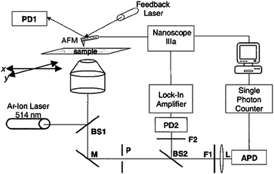 | ||
| Fig. 1 A schematic diagram of the experimental setup for correlating fluorescence and AFM. Key: BS1, BS2, Beam splitters; M, mirror; P, pinhole; F1, F2, optical filters; L, lens; PD1, AFM feedback detector; PD2, Si photodiode detector. (L. A. Kolodny et al., Anal. Chem., 2001, 73, 1959–1966; copyright 2003, American Chemical Society. Reproduced with permission.) | ||
The above-described experimental design permits an image lateral resolution of ∼10–20 nm. Superposition of these optical and topographical images enables unambiguous identification of the sample topography residing within the excitation region of the optical microscope, thus facilitating the 3D morphology characterization of the NPs or the fluorescence signal from the response of a bio-molecule. These measurements also provide the lateral position of the NP relative to the laser excitation profile and the surrounding topography with nanometre-scale precision. It also permits investigation of the relationship between the spectroscopic and structural properties of individual NPs.
Kolodny et al. have used this method to probe fluorescent polystyrene nanospheres.27 The method can be used to correlate the fluorescent properties of fluorescent nanospheres, as small as 20-nm in diameter, with their topographies. Nie and Emory used this design to investigate the size, shape and aggregation-dependent Raman enhancement efficiency of Ag NPs by combined AFM and Raman scattering spectroscopy,30 which also preserves the possibility of studying the size-dependent physicochemical properties of single organic nanostructures31 and semiconductor nanocrystals.32
A second in situ method has been demonstrated by Nalayah et al. that is based on utilizing the electron beam in a scanning transmission electron microscope (STEM) to probe the high-angle annular dark-field (HAADF) signal.1 This method allowed them to construct the topography of individual NPs and perform electron energy-loss spectroscopy (EELS) for plasmon signal measurement of the same NPs. This method relies on the detection of plasmons as resonance peaks in the energy-loss spectra of sub-nanometre electron beams rastered on the NP. The EELS measurements can be carried out in a VG-HB501 STEM operated at 100 kV and fitted with a Gatan 666 spectrometer. The EELS spectra are recorded using the so-called spectrum-imaging mode, in which a 1-nm-diameter focused electron probe is rastered, with a constant spatial displacement of 1 to 4 nm over the sample. At each point of the raster, a number of spectra (typically 50) will be acquired, with a dwell time per spectrum as short as 3 ms, in parallel with the HAADF signal for surface topography imaging. This is shown in Fig. 2a. This method has the ability to detect the EELS spectra of specific local position on the NP. Fig. 2b shows the evolution of the spectra as the electron probe is scanned along an axis of the NP for 32 successive recordings of low-loss STEM–EELS spectra for the Ag NP. The fast acquisition rate of this detection system, together with the high brightness and small energy dispersion of the cold field-emission gun, made it possible to detect the presence of peaks at energies as low as about 1 eV. By utilizing electrons instead of photons as a probe, this in situ STEM-EELS method can map the spatial variation of localized surface plasmon resonances of specific single NPs with spatial accuracy up to λ/40, where λ is the corresponding wavelength of the excitation. This represents a significant improvement in the spatial resolution with which plasmonic modes can be recorded and provides a powerful tool in the development of nanometre-level optics.
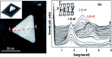 | ||
| Fig. 2 Scanning transmission electron microscopy and electron energy loss spectroscopy (STEM–EELS) measurements on an equilateral Ag nanoprism with edge length of 78 nm. (a) high-angle annular dark-field (HAADF)–STEM image of the particle, showing the regular geometry that is characteristic of most triangular particles synthesized in this sample. The projected mass image of the scanned region shows the flat top and bottom morphology of the particle (inset). The image contrast around the particle is due to radiation damage in the mica caused by the electron beam. (b) A series of 32 successive low-loss STEM–EELS spectra acquired, in the spectrum-image mode, along an axis (A to B) of the nanoprism, as illustrated in the inset. The positions of the three main resonances detected along the line scan are marked by dotted lines. (J. Nelayah et al., Nat. Phys., 2007, 3, 348–353; copyright Nature Publishing Group. Reproduced with permission.) | ||
While the above-mentioned in situ method provides valuable information on NP properties, it does not allow the characterization of an individual NP even when used in combination with other techniques such as TEM, SEM, fluorescence microscope, or dark field microscope because it is notoriously difficult to find the same NPs after the sample is transferred from one instrument to the other.7,27 To be able to use multiple characterization techniques, precise methods of locating the same NP are needed. This is accomplished in the spatial-localization methods discussed next.
2.2 The spatial-localization methods
The following discussion focuses on the development of spatial-localization methods for the correlation of 3D morphologies and optical properties of single NPs or nanoparticle arrays based on Ag NPs as a model. In order to precisely correlate the optical spectra of individual silver NPs to their geometrical shapes, Schultz et al. have developed a method that is based on the relative position of Ag NPs in the viewed field as position markers.28 The optical properties can be characterized after the sizes and shapes of NPs are imaged by TEM.28 The sample is first examined by an optical microscope modified for single-particle spectroscopy. To obtain the plasmon resonance spectrum from one individual silver NP, un-polarized light from a Xe source (75 W) is incident on the particle using dark-field illumination. The light scattered from the nanoparticle is then directed to an image plane aperture of ∼0.2 mm diameter to reduce scattered light from other regions of the sample arriving at the detector. In order to have a spatial map of the relative locations of the particles, a wide-field optical image containing approximately 100 particles is recorded. This image is subsequently used as a pattern-recognition template during the TEM analysis to correlate the color and spectral responses of the particles with their shape and size, which can be imaged and analyzed by TEM. Then, recognizable features of the sample found in the wide-field optical microscope image can be directly correlated to the same features seen on the electron microscope fluorescent screen by visual inspection during the TEM examination. One example of well-identified NPs and NP pairs imaged by TEM and dark-field microscopy is shown in Fig. 3. From the position and orientation of the NPs in the TEM images and dark-field images, correlation of the nanoparticles in both images can be made. The NP morphologies, including their 3D topography obtained by tilting the sample, can be characterized by high resolution TEM. Therefore, correlation between the color and LSPR spectrum of the specific NPs and their sizes, shapes, and 3D morphologies can be made. The results suggest that with increasing particle size the corresponding spectra are red-shifted. Based on the experimental results obtained from high resolution TEM images at normal beam incidence for NPs of 40–120 nm, most of the particles that image as a triangle appear red, particles that image as a pentagon appear green, and particles that image as a circle (roughly spherical) appear blue. Fig. 4 shows a plot illustrating the relationship between the size and shape (as determined from the TEM image) and the spectral peak wavelength for a diverse collection of individual silver NPs. Representative TEM images for three particles with different sizes, for each geometrical shape, are also shown in the top of Fig. 4. A significant scatter due to the shapes of the triangular particles is evident in Fig. 4. By tilting the angle of the sample with respect to the electron beam in the TEM, the 3D morphology for the NPs can be determined. Observation of the morphologies of these silver NPs at different tilting angles indicates that the scatter in the size of the triangular particles, although having similar spectral peak wavelengths (as seen in Fig. 4), is clearly due to different morphologies in the third dimension of the tetrahedron-shaped NPs.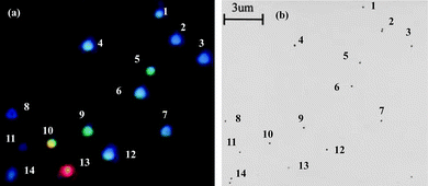 | ||
| Fig. 3 (a) An electronic camera (Nikon Coolpix 950) color image of a typical sample of silver NPs as viewed under the dark-field microscope. The brightness of the particles increases from blue to red due to both the intrinsic optical scattering cross-section and the spectral output of the light source. As a result, the red particle is overexposed. This image can be subsequently used as a pattern recognition template during the transmission electron microscopy (TEM) analysis. (b) A bright-field TEM image of the same collection of silver NPs. (J. J. Mock et al., J. Chem. Phys., 2002, 116(15), 6755–6759; copyright (2002) American Institute of Physics. Adapted with permission.) | ||
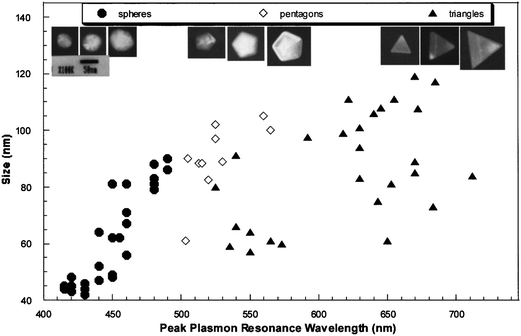 | ||
| Fig. 4 TEM lateral size versus the spectral peak wavelength for several individual silver NPs. The size of each nanoparticle is assigned by the TEM image taken with the electron beam normal to the sample. The characteristic dimension for a spherical particle (circular image) is the diameter, for a pentagon it is the length between opposite corners, and for a triangle it is the length of a side. Typical colloidal sample color population is approximately as follows: 85% of the particles are blue, 5% of the particles are green, 5% of the particles are red, and 5% of the particle population has a broad or dual-peak spectral signature that indicates clustering or other complex shapes. Representative TEM images for three different size particles, of each geometrical shape, are also shown (top images). (J. J. Mock et al., J. Chem. Phys., 2002, 116(15), 6755–6759; copyright (2002) American Institute of Physics. Adapted with permission.) | ||
Correlation of optical and TEM images of individual NPs using enumerated TEM grids and fabricated position markers on a Si3N4 thin-film window supported on a silicon wafer has been reported.26,28,33Fig. 5 shows an example where the fabricated position markers are used to identify the NPs and correlate them with their second harmonic generation (SHG). Fig. 5a shows a TEM image of a position marker pattern consisting of microbars and nanodots. A zoomed-in area is shown in Fig. 5b. The Si3N4 window substrate with position markers can be used in absorption, scattering, and nonlinear optical measurements. Using this position-marker pattern, Jin et al. demonstrated correlation of SHG of single Ag NPs or Ag aggregates with their precise structure imaged by TEM.26 The SHG map (e.g., Fig. 5c) can be acquired with a nonlinear optical microscopy system consisting of an inverted microscope and a tunable femtosecond pulsed laser (e.g.,Ti: sapphire laser). Prior to the SHG measurements, a bright field image of the marked area of the sample was acquired with white-light illumination from a halogen lamp. The sample position is then mechanically fixed and the femtosecond laser pulses will be introduced. Careful adjustment of the focal plane ensures an optimized second harmonic (SH) signal from the specific Ag NPs. Fig. 5c shows the SH image of Ag NPs for the identical area as in Fig. 5b. Emission spectra, laser polarization, and excitation wavelength dependence confirms that the detected signals are SH activity and not two-photon fluorescence. Results obtained by Scherer et al.34 indicate that NPs with a non-spherical shape (e.g., Ag nanorods) exhibit much greater SH activity than isolated single quasi-spherical NPs (Fig. 5d). The direct and precise correlation of the structure and SH activity and other spectral properties leads to the conclusion that the SH signal from the highly active Ag nanostructures (i.e., nanorods, touching dimers, and clusters) arises from one-photon resonant excitation of the longitudinal plasmon mode of the nanorods or dimers.34 Using NP position markers that rely on forming unqiue random patterns by a group of NPs, allows recognition and imaging, using both optical and electron microscopy, to identify a single NP of interest.
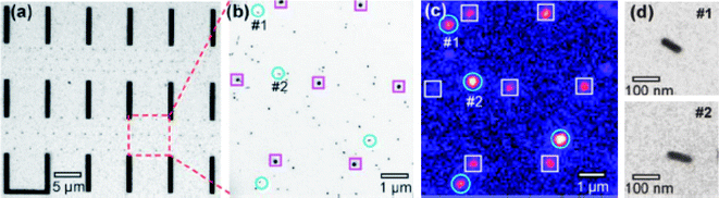 | ||
| Fig. 5 (a) TEM image of a position-marker pattern consisting of bars and nanodots. (b) 5× magnified view of a region in (a). (c) SH optical image (false color image) of the same area as (b). The circled spots in (b) and (c) are single Ag nanorods giving SH signals. The spots marked by squares forming a hexagonal pattern are the dot markers (∼100 nm diameter). d: Zoomed-in images of single nanorods #1 and #2 shown in image (b). (R. Jin, et al., Appl. Phys. Lett., 2006, 88(26), 263111; copyright (2006) American Institute of Physics. Reproduced with permission.) | ||
The above approach cannot be used to study any desired set of NPs that may not form a recognizable pattern or that are separated by distances less than what can be resolved due to the optical diffraction limit. In the position-marker-pattern method,26 it is also not possible to characterize the NPs in a living organism since TEM and SEM are operated in high vacuum. TEM and STM are not best suited to provide quantitative 3D morphologies of individual NPs. Therefore, it is important to develop effective methods to precisely locate and identify a single NP of interest and characterize its morphology and optical property.
Recently, Song et al. have developed a technique to identify the location and orientation of single Ag NPs using multi-hierarchy arrayed micro windows fabricated on the substrates (e.g., glass cover slip). This technique permits easy characterization of the 3D morphologies of single NPs based on AFM and their LSPR spectra using dark-field microscopy and spectroscopy. It is also possible to investigate the local morphology dependence of the LSPR spectra of the single NPs.7,17
In this method, multi-hierarchy arrayed micro windows are first fabricated on a glass cover slip using the standard photolithography.7,35,36 The main steps in the process are shown in Fig. 6.7,17 A two-layer structure (Fig. 6(a)) for printing the micro arrays by UV lithography is first coated on the substrate, which is fabricated by depositing a layer of chromium on the sample platform, followed by spin-coating a layer of positive photoresist on top of the chromium layer (Fig. 6(b)). Next, the 2-layer structure of the substrate is shaded with an optical mask on top of the photoresist layer and exposed to UV light for 10–60 s to form the micro-patterns in the photoresist layer. Then, the exposed areas of the photoresist layer are developed by photoresist developer to leave the bare chromium areas (Fig. 6(c)). In the fourth step, the bare Cr areas are etched away by a Cr etcher to form the desired micro window array on the sample platform (Fig. 6(d)). Finally, the undeveloped photoresist is removed using acetone, leaving the desired micro window arrays formed in the Cr layer on the substrates (Fig. 6(e)), with each unit having several distinct transparent windows (Fig. 6(f)).
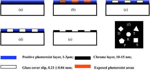 | ||
| Fig. 6 The UV lithography process to fabricate the multi-hierarchy micro arrays on the glass cover slip. (a) The 2-layer structure of the substrate for printing the micro arrays by UV lithography includes a 1–3 μm positive photoresist (Shipley Microposit) layer and a 15–20 nm chromium layer on the glass cover slip. It was fabricated by first depositing a layer of chromium on a clean glass cover slip followed by spin coating of the positive photoresist on top of the chromium layer. (b) The 2-layer structure of the substrate was covered with an optical mask on top of the photoresist layer and exposed to UV light for 10–60 s to form the micro-patterns in the photoresist layer. (c–d) The exposed areas of the photoresist layer were developed by photoresist developer (MF-321, Shipley Microposit) to leave the bare chromium areas, which were then etched away by Cr etchant (Cyantek) to form the desired micro arrays on glass. (e–f) The undeveloped photoresist was removed using acetone, leaving the desired micro arrays formed in the Cr layer, with each unit having 5 distinct transparent windows. The nanoparticles were fabricated by nanosphere lithography. This process can also be done by electron beam lithography for feature resolution in the tens of nm. | ||
Fig. 7(a) and 7(b) show examples of the design of the multi-hierarchy arrayed micro windows (there are 3 tiers) and the typical final micro windows (Fig. 7(c)) pattern after printing.7,17 The multi-hierarchy arrayed micro windows on the glass cover slip are used to identify the location and orientation of single NPs, whose tiers can be determined by the observed field at desired resolution. For example, in the first tier of the multi-hierarchy arrayed micro windows (Fig. 7(a)), each local area can be discerned by marking its X and Y number, such as the shaded area X1–Y2. Then, in the second tier of the multi-hierarchy arrayed micro windows (Fig. 7(b)), the scale can be reduced by M or N times and each local area can also be marked by x and y number. If this area is the sub-tier in the shaded area of the first tier, it can be labeled as X1–Y2–x3–y3. In a similar way, step-by-step, we can reach the last tier with several transparent micro windows available (Fig. 7(c)), in which the desired nanoparticle can be made by different fabrication methods (e.g., electron beam lithography or nanosphere lithography). Nanoparticles less than 10 nm of different shapes synthesized by a wet-chemical process can be immobilized by a routine diluted deposition process. Consequently, the same nanoparticle in each window can be identified by comparing the images taken by the optical microscope with those characterized by the AFM. Finally, in each window, the same nanoparticle can be characterized by different techniques (e.g., the dark-field optical microscope and spectroscopy (DFOMS) and AFM) allowing correlation of its 3D morphology with its optical response.7,17
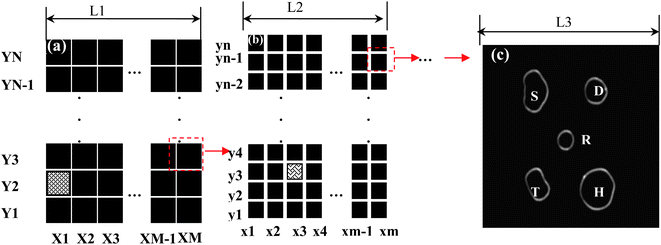 | ||
| Fig. 7 The multi-hierarchy arrayed micro windows on the substrate (e.g., glass cover slip). (a) The first tier of the multi-hierarchy arrayed micro window, each local area can be discerned by marking its X and Y number, such as the red area of X1–Y2. (b) The second tier of the multi-hierarchy arrayed micro windows, whose scale can be reduced by M or N times, whose local area can also be marked by x and y numbers. If this area is the sub-tier in the red area of the first tier, it can be labeled as X1–Y2–x3–y3. Step-by-step, the last tier with several unique-shaped transparent windows can be reached. The open windows can be made with different shapes. (c) The nanoparticles can be fabricated on the micro-pattern by various methods (e.g., nanosphere lithography). In each window, the same nanoparticle can be identified by comparing the images taken by optical microscopy, AFM, or other microscopy methods. Finally, the structural parameters (size, shape, orientation, interparticle spacing, and thickness) can be correlated with their optical responses (Y. Song, et al.J. Phys. Chem. C, 2010 114, 74–81; copyright (2010) American Chemical Society. Adapted with permission.) | ||
A typical example to identify single NPs using both AFM and DFOMS is illustrated in Fig. 8.17 Single Ag NPs fabricated on the surface of glass cover slips within the hexagonal micro window were identified and characterized using AFM (Fig. 8(a-1)) and DFOMS equipped with a color camera (Fig. 8(b-1)) and charge-coupled device (CCD) camera (Fig. 8(c-1)). The CCD camera offers higher spatial resolution than the color camera, while the color camera provides the real colors of individual Ag NPs that are generated by LSPR. The square area in Fig. 8(a-2) contains several NPs and is shown expanded in Fig. 8(b-2). The center of each individual NP in the optical images recorded by the CCD is located with a single-pixel resolution (each pixel can be 125 nm or 67 nm depending on the CCD resolution and equipment setup) by determining the address of the pixel with the highest intensity of the NP. The positions of individual NPs of interest within the micro window in the optical images (Fig. 8(b-2) and (c-2)) are then determined with a spatial resolution limited by the optical diffraction limit (∼200 nm) and an orientation angle resolution of about 0.5 degree. This approach allows us to correlate AFM images of individual NPs (as the one circled in Fig. 8(a-2)) with the same NP shown in its corresponding optical image (circled in Fig. 8(b-2) and (c-2)) and to investigate their 3D morphological-dependent LSPR properties.
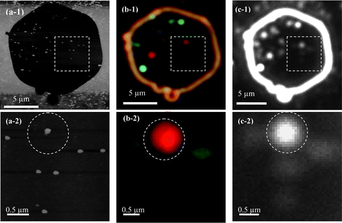 | ||
| Fig. 8 Correlation of AFM and optical images of single Ag NPs using the micro-patterned windows: (a-1) AFM images, (b-1) optical true-color images and (c-1) CCD images of single Ag NPs in a hexagon micro-patterned window, respectively; magnified images of individual NPs squared in (a-1, b-1, c-1), showing the correlation of (a-2) AFM images of given single NPs at nanometre scale with (b-2) optical true-color images and (c-2) CCD images of single Ag NPs at micrometre scale, as illustrated by the circled NP. Note that the scale bars in (b–c) show the distances among individual NPs, but not the sizes of single NPs because they are imaged under the optical diffraction limit (Y. Song, et al.J. Phys. Chem. C, 2010 114, 74–81; copyright (2010) American Chemical Society. Adapted with permission.) | ||
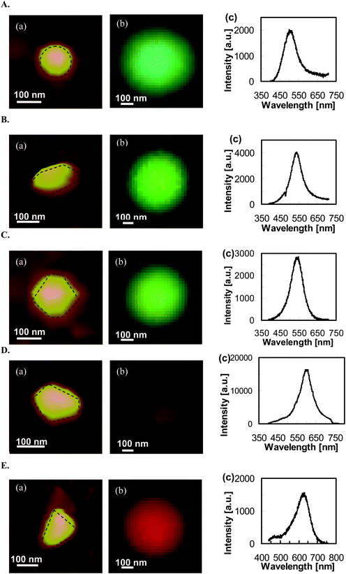
This new methodology allows the selection of a variety of individual NPs and characterization of their 3D morphologies and LSPR spectra using AFM and DFOMS, with the aim to determine their shape-dependent LSPR spectra. Fig. 9 shows a set of silver NPs with nearly equal volume and cross-section, but with different shapes. AFM images of individual NPs (Fig. 9(A–E: a)) show a variety of shapes, including (A: a) quasi-circular cylindrical; (B: a) oblate spheroid; (C: a) irregular-hexagonal cylindrical; (D: a) quasi-pentagonal cylindrical, and (E: a) quasi-trapezoidal cylindrical. Their optical images and LSPR spectra measured using DFOMS (Fig. 9(A–E: b–c)) show peak wavelengths (λpi) of 506, 537, 548, 603, and 629 nm, respectively, with a shoulder peak wavelength of 470 nm. Nonetheless, the true colors of individual Ag NPs reflect their LSPR responses, as illustrated by their LSPR spectra (Fig. 9(A–E: c)). The experimental results in Fig. 9 clearly demonstrate shape-dependent LSPR spectra of single Ag NPs. As in the previous investigation on shape-dependent optical properties of NPs based on the ensemble methods,28 and DDA simulation,9,37 the peak wavelengths of LSPR spectra of single Ag NPs gradually shift to the longer wavelength (red-shift) as the shape of the NPs deviates significantly from the circle shape to the polygon shape, and the tips of the NPs become sharper.
 | ||
| Fig. 9 Characterization of shape-dependent optical properties (LSPR spectra) of single Ag NPs determined using experimental measurements and theoretical calculations. (A–E): (a) AFM images, (b) dark-field optical color images, and (c) experimental measured LSPR spectra. All scale bars are 100 nm. Note that the scale bars in (b) are used to measure the size of image arrays, but not the sizes of single NPs because the NPs are imaged under optical diffraction limit. (Y. Song, et al.J. Phys. Chem. C, 2010 114, 74–81; copyright (2010) American Chemical Society. Adapted with permission.) | ||
To investigate the effects of the 3D morphology of single Ag NPs on their LSPR spectra, the 3D morphology of a selected single NP was characterized using AFM. The AFM images in Fig. 10(a,b) show an NP with one sharp tip and three curved corners, with the width of the cross-section (measured from the tip to the opposite edge of the NP) equal to 210 nm and the NPs have a variety of heights ranging from 10 to 60 nm. The optical image of the NP acquired using DFOMS (Fig. 10(c)) and the 3D plot of the distribution of the scattering intensity of the NP versus its x–y dimension (Fig. 10(d)) illustrate the strong location dependence of the scattering intensity of the NP. The color image and LSPR spectrum of the NP in Fig. 10(e) show the primary peak wavelength at 630 nm (red color) and two weak shoulder peaks at 524 nm and 465 nm, respectively. Comparing this result with the DDA simulation on a snipped triangle nanoprism,14,38 it is believed that the peak at 630 nm is attributed to the in-plane dipole plasmon resonance, while the peaks at 524 nm and 465 nm are generated by the in-plane and out-plane quadrupole plasmon resonance, respectively. Since the intensities of the in-plane and the out-plane quadrupole plasmon resonance (524 and 465 nm) are much weaker than the in-plane dipole plasmon resonance (630 nm), the NP has a red color under dark-field microscopy, which is attributed by the primary peak of the LSPR spectra (Fig. 10(f)).
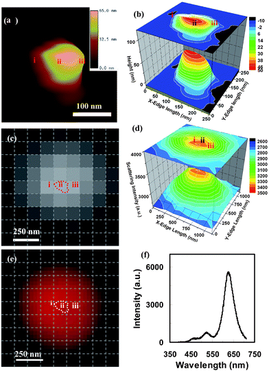 | ||
| Fig. 10 A single polygon (5) mono-color silver nanoparticle with 56.4 nm out-of-plane thickness was characterized using AFM and dark-field optical microscopy and spectroscopy. (a) AFM, (b) the magnified 3D contour of the AFM image, (c) the CCD image for recording the local LSPR spectra, (d) the light-scattering intensity spectra around the nanoparticle, (e) the color image, and (f) the LSPR spectrum for the whole nanoparticle. In order to identify the location and the orientation of these positions around the nanoparticles, the CCD image and color image were netted by dashed lines with each square unit of 125 × 125 nm after their distances and orientations were corrected. The spectrum of the whole particle gave multi-mode spectrum with three peaks (f), suggesting an in-plane dipole plasmon resonance at 625.9 nm, an in-plane quadrupole plasmon resonance at 525.7 nm, and an out-plane quadrupole plasmon resonance at 464.7 nm. Since the intensities of the last two peaks were much lower than the first one, this particle still showed a mono-color dominated by the in-plane dipole plasmon resonance. (Y. Song, et al.J. Phys. Chem. C, 2010 114, 74–81; copyright (2010) American Chemical Society. Adapted with permission.) | ||
From Fig. 10(c) and (e), we note that the optical images of the NP appear to be larger than its actual size, and show much lower resolution than the one determined by AFM (Fig. 10(a)), due to the optical diffraction limit. However, using the method described in Fig. 10, the AFM and optical images in Fig. 10 are well correlated and aligned on the same orientation. Using the position of the pixel with the highest scattering intensity and intensity-distribution profile of the NP (Fig. 10(a, c, e)), the LSPR spectra at different locations above this NP can be investigated. The LSPR spectra at three different locations around this NP have been recorded, as marked in its CCD image (Fig. 10(c)), the correlated AFM (Fig. 10(a)), and in the color image (Fig. 10(e)), for example. These local LSPR spectra are plotted in Fig. 11. The peak wavelengths and intensities are summarized in Table 1, clearly showing significant location-dependent LSPR around this irregular shaped single nanoparticle. The scattering intensity at the center part of this NP gives the highest value. Although the simulation result indicates that the tip effect may enhance the local electrical field and give a red shift in the peak wavelength,37 the peak wavelength in this NP shows a blue shift when the recorded location approaches the tip, as indicated by the peak wavelengths collected above the tip area (Fig.11-i: 622 nm), the center area (Fig.11-ii: 624 nm) and the corner area (Fig.11-iii: 628 nm). Since the local 3D morphology could be correlated with their local LSPR spectra, it is clear that the decrease in thickness from the tip to the corner may contribute to this LSPR peak wavelength shift that is also consistent with the discrete dipole approximation (DDA) simulation of the NP thickness effect.37 For locations away from the center of this Ag NP, the peak line widths for the dipole resonance mode become larger due to the radiative damping and the enhanced interaction with the substrates, while the peak line widths for the quadrupole resonance change little.
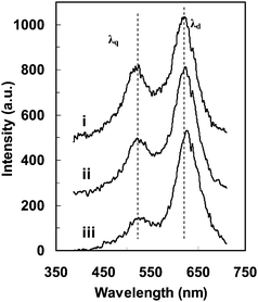 | ||
| Fig. 11 The LSPR spectra at individual locations (i, ii and iii) in the single nanoparticle in Fig. 10 showing anisotropic optical responses due to the variation in local 3D morphology and the orientation of the specific local 3D morphology. (Y. Song, et al.J. Phys. Chem. C, 2010 114, 74–81; copyright (2010) American Chemical Society. Adapted with permission.) | ||
| Locationa | λ d/nm | λ q/nm |
|---|---|---|
| FWHM/nm | FWHM/nm | |
| a Locations are marked in the CCD pixel array in Fig. 10 c and e. λd and λq are the primary and the shoulder peak wavelength of LSPR spectra in Fig. 11, representing the dipole plasmon resonance and the quandrupole plasmon resonance. | ||
| i | 622 | 526 |
| 52 | 42 | |
| ii | 624 | 522 |
| 42 | 40 | |
| iii | 628 | 524 |
| 54 | 42 |
Fig. 12(a) is an AFM image of a silver NP showing that it has a short rod shape with a longitudinal dimension of 420 nm, a transverse dimension of 220 nm, and an out-of-plane thickness of 121 nm.17 Its real color image, taken by a color camera connected to the dark-field microscope, gives a multi-color feature (Fig. 12(b)). The DDA simulation shows excellent agreement with this result. The LSPR spectrum of this simulated NP shows two distinct peaks, at 510 nm and 610 nm (Fig. 12(c): triangle labeled line), representing the longitudinal and transverse dipole plasmon resonance in the quasi-semi-nanorod, respectively, which are near the observed peaks in the experimental spectrum (wide solid line in Fig. 12(c): 513.4 nm and 604.8 nm). The shape resonance of the experimental spectrum also matches the DDA simulation, with almost the same peak intensity ratio (Table 2). However, the two weak shoulders at 555 nm and 650 nm predicted by the DDA calculation in Fig. 12(c), representing the longitudinal and transverse quadruple resonance, respectively, were not detected. This is probably due to their weak signals that are suppressed by the two main intense LSPR modes or due to coupling effects among the irregular surface morphology in the real NP. DDA simulations for one semi-ellipsoid and one triangular nanoprism have been performed (image data not shown here), which also show a good match with the experimental results.39
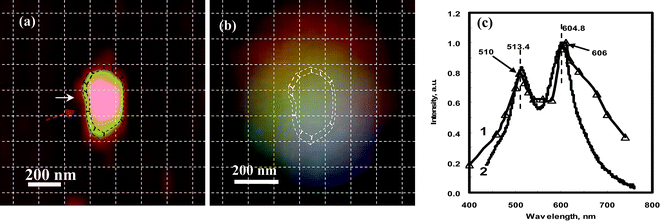 | ||
| Fig. 12 (a) AFM image for one quasi-semi-rod shaped Ag nanoparticle with a longitudinal dimension of 420 nm, a transverse dimension of 220 nm, and the out-of-plane height of 121.6 nm; (b) the real color image of the nanoparticle observed by optical microscopy; (c) the LSPR spectrum for the whole NP. In (c) the wide solid curve is the experimental curve after correcting for the instrumental response at different wavelengths; the thin triangles is the DDA calculation. The spectrum of the whole particle gives a dual-peak spectrum at 513.4 nm and 605.8 nm, which shows good match with the DDA simulation (see Table 2 for data). Note: the DDA calculation was performed by Zongsuo Zhang and Ququan Wang at Wuhan University and the result was discussed and confirmed with Haining Wang and Shengli Zou at Florida Center University. In order to identify the location and the orientation of these positions around the NPs, the AFM image and color image were netted by dashed lines with each square unit of 125 × 125 nm after their distances and orientations were corrected. (Adapted from reference Y. Song, China Patent, Appl. No. CN200910085973.9). | ||
| Shape of nanoparticles | Quasi-semi-ellipsoid | Quasi-semi-rod | Triangle nanoprism | |
|---|---|---|---|---|
| a Exp: measured by experiments; Modified: LSPR curve modified according to the instrumental responsivity at different wavelengths and the quantum efficiency at different wavelengths; DDA: calculated by the DDA method. | ||||
| λ 1, nm | Exp | 680.2 | 514.7 | 562.3 |
| Modified | 680.2 | 514.7 | 557.8 | |
| DDA | 680.2 | 512.1 | 540.0 | |
| FWHM1, nm | Exp | 116.4 | 40 | 46 |
| Modified | 112.0 | 41 | 46 | |
| DDA | 96.0 | 47 | 35 | |
| λ 2, nm | Exp | NA (not available) | 602.2 | 659.9 |
| Modified | NA | 605.4 | 664.2 | |
| DDA | NA | 607.3 | 662.0 | |
| FWHM2, nm | Exp | NA | 39 | 48 |
| Modified | 39 | 48 | ||
| DDA | NA | 61 | 80 | |
| λ 3, nm | Exp | NA | NA | 759.6 |
| Modified | NA | NA | 763.1 | |
| DDA | NA | NA | NA | |
| FWHM3, nm | Exp | NA | NA | 40 |
| Modified | NA | NA | 40 | |
| DDA | NA | NA | NA | |
Ratio of peak intensity (λ1![[thin space (1/6-em)]](https://www.rsc.org/images/entities/char_2009.gif) :λ2:λ3) :λ2:λ3) |
Exp | NA | 0.85:1.0 |
0.91:1.0:0.55 |
| Modified | NA | 0.83:1.0 |
0.92:1.0:0.58 |
|
| DDA | NA | 0.80:1.0 |
0.94:1.0:0.47 |
|
Fig. 13 gives the AFM images of two other specific shaped Ag NPs (quasi-semi-ellipsoid and triangle nanoprism) characterized by multi-hierarchy arrayed micro windows,17 whose LSPR peak positions and FWHMs are summarized in Table 2. The AFM image of the quasi-semi-ellipsoid silver NP shows that it has a long axis of 280 nm, a short axis of 196 nm and an out-of-plane height of about 26.8 nm (Fig. 13(a,b)). This NP only shows one mono peak at 680.2 nm. Their peak wavelengths (λi), peak ratios, and line widths (FWHM) from experiment are in good agreement with DDA simulation, as summarized in Table 2. In general, the DDA simulation shows best agreement with the experimental spectra for NPs, hence their shapes can be accurately modelled. However, it can also be seen that for wavelengths longer than 650 nm, the experimental results have a lower intensity than the simulation (ratios of peak intensities in Table 2). This is expected to be mainly due to the errors from the spectrometer responsivity and the wavelength-dependent CCD quantum efficiency.40 However, when the effects from the spectrometer and the wavelength dependent CCD quantum efficiency are included in these measurements (the data shown as “Modified” in rows of Table 2), there are still visible deviations between the DDA calculation and the modified results. In addition, the deviations between the peak positions for complex-shape NPs (e.g., quasi-semi-rod and triangle nanoprism) are still larger than the simple-shape NPs (e.g., quasi-semi-ellipsoid). These deviations are probably caused by the precision in the shape construction during DDA simulations.
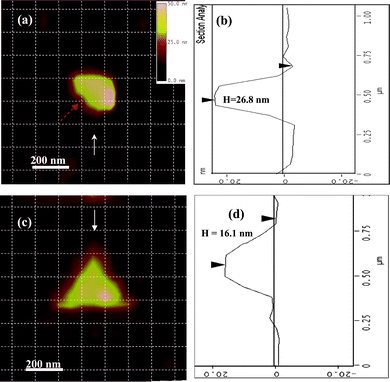 | ||
| Fig. 13 AFM images of two other specific Ag NPs for LSPR measurement. (a) the AFM image for a quasi-ellipsoid-shaped Ag nanoparticle with long axis of 280 nm and short axis of 196 nm; (b) the height mapping of the quasi-ellipsoid-shaped Ag nanoparticle along the direction of the arrow in Fig. 12(a), showing the out-of-plane height of this nanoparticle about 26.8 nm; (c) the AFM image for one triangular-shaped Ag nanoparticle with average edge length of 383 nm; (d) the height mapping of the triangle shape Ag nanoparticle along the direction of the arrow in Fig. 12(c), showing the out-of-plane height of this nanoparticle of 16.1 nm. In order to identify the location and the orientation of these positions around the NPs, the AFM image and color image were netted by dashed lines with each square unit of 125 × 125 nm after their distances and orientations were corrected. (Adapted from reference Y. Song, China Patent, Appl. No. CN200910085973.9). | ||
From these results, it was also found that when the shapes and 3D morphologies of the NPs became more complicated, the deviation between the DDA simulation and the experimental result increased. This is due to the geometrical deviation between the real NPs and the regular species used in the calculations. It can also be seen from the experimental results that the intensity beyond the 550–650 nm range is decreased compared to the simulation results. This is probably due to the different quantum and instrumentation efficiencies.40 According to the quantum efficiency and instrument efficiency of the EMCCD data, both of the two efficiencies are higher at 550–650 nm than at wavelengths beyond this range. If these two instrumental factors are considered, the corrected experimental results have a good match with the DDA simulation. This confirms that our experimental method, based on the far-field detection, preserves the ability to detect the near-field LSPR signal.
The new methodology, based on the multi-hierarchy arrayed micro windows that we have developed can be used to correlate effectively the optical image of single Ag NPs with their AFM images. This enables us to characterize optical properties (e.g., LSPR spectra) of single Ag NPs at sub-micrometre resolution (∼200 nm or less) using DFOMS and their 3D morphologies at nanometre resolution using AFM. The approach allows us to investigate shape-dependent LSPR spectra of single Ag NPs. We have found that the LSPR spectra of single Ag NPs exhibit dependence on their shape, even though these individual NPs have nearly equal volume, cross-section and height. In general, the experimental measurements of the shape-dependent LSPR spectra of single NPs agree very well with DDA simulation results. It is also found that the simulation data of simple shaped NPs have better agreement with the experimental results than those of complex-shaped NPs. The reason for this lies in the construction of exactly identical shapes using current methods. Furthermore, we can locate the position of a single NP in an optical image by correlating its optical image with the AFM image. This permits us to measure the LSPR spectra of single NPs at different locations and also to investigate the surrounding regions. This capability makes it possible to investigate the effect of the local medium on the optical properties of the NPs. The result shows location-dependent LSPR spectra of a single NP on its surrounding area. This offers a unique opportunity to characterize individual multi-mode plasmonic NPs at nanometre resolution for better understanding of the optical properties of single NPs and rational design of single NP plasmonic optical probes. The above results also indicate that some of the near-field features on the LSPR of Ag NPs can be discerned by the far-field DFOMS method. This methodology provides an effective means to investigate 3D morphological dependent LSPR spectra of single NPs, thus offering valid experimental data for better understanding of the effects of 3D morphologies on optical properties of individual NPs. This adds to the simulation methods that can accurately describe optical properties of NPs with complex morphologies.
This approach, based on multi-hierarchy arrayed micro windows, also has importance when fabricating the desired kind of windows on TEM grids or other sample supporters for characterization of other physicochemical properties of NPs and NP arrays by other instruments (e.g., electrical properties or magnetic properties). This approach may open more efficient instrumentation for the investigation of the 3D morphologies and space orientation dependent physicochemical properties in addition to the optical properties of NPs. The size of these micro windows can also be controlled by using nanofabrication instrumentation with high resolution (e.g., electron beam lithography with a resolution up to 30 nm). The size of a NP that is located in the micro windows can also be reduced to below 10 nm by using a suitable method for size control (e.g., wet-chemical process). The 3D morphology and space orientation dependent physicochemical properties of specific individual NPs and nano-arrays can be precisely investigated by immobilizing the desired NPs and NP arays in these micro windows.
3. Summary
In this article, the progress in the identification of individual NPs and correlating their optical properties with their 3D morphologies has been reviewed. Both the in situ and the spatial-localization methods are described. Some in-situ methods developed based on combining AFM and optical microscopy27 usually result in relatively low-spatial resolution. An in situ method with much high resolution has been developed by combining scanning transmission electron microscopy (STEM) for morphology characterization of the NPs and the electron energy loss spectroscopy (EELS) for probing the related electronic properties (STEM-EELS method).1 Although the instrumentation is relatively expensive for the STEM-EELS method, it can provide spatial resolution up to a nanometre. For the identification of the surface plasmon resonances of single NPs, the light wavelength can be expanded from the near-infrared range, to the visible, and to the ultraviolet with a spatial resolution up to λ/40 (λ: the wavelength of the related excitation).1The spatial-localization method can allow for NP probing with different techniques. The development of spacial-localization probing technology relies on locating a specific NP using some type of position marker. This allows measurement of the optical properties of the NP by dark-field microscope and then characterization of their sizes and shapes by TEM or AFM. A spacial-localization method is based on the multi-hierarchy arrayed micro windows, which are similar to a multi-dimensional matrix that makes the re-localization of the same single NPs by different instruments more convenient. This method also eliminates signal aberration due to the interaction between the probes and NPs in in situ methods. Based on advanced micro/nanofabrication technology, the sizes of these micro windows can be reduced to the nanoscale and the substrates for the support of these micro windows can be flexible (e.g., glass, mica, or carbon-coated TEM grids). The multi-hierarchy arrayed micro window method of single-NP identification can potentially be used to correlate 3D NP morphologies of single NPs with their optical, electronic, and magnetic properties. It should be pointed out that the recent progress in single-nanoparticle identification obtained by DFOMS and EMCCD assisted by multi-hierarchy arrayed micro windows indicates that this kind of far-field detection technique preserves the ability to detect the signals from the near-field LSPR, which are usually observed by near-field detection techniques (e.g.,scanning near-field optical microscopy, SNOM).
4. Perspectives
The development of methodology for single-nanoparticle identification makes it possible to investigate the size, shape, and location-dependent properties of nanoparticles at high resolutions (e.g., nanometre or even subnanometer). For example, the STEM-EELS method has realized the feasibility of mapping the spatial variation of localized surface plasmon resonances of specific single NPs in the near-infrared, visible, and ultraviolet range and with a nanoscale spatial resolution.1 Many interesting novel phenomena have been observed that can be explained perfectly by correlating the size, shape and local 3D morphologies of these NPs with their chemical properties. This provides valid experimental evidence for the confirmation and development of nanoscale theory.1,27,28,41Development of single-nanoparticle identification techniques also advances applications of single-nanoparticle sensors, such as in single NP biosensors.17,27 These sensors can be more precise, ultra-sensitive, target-oriented, and environmentally friendly since they are easily functionalized digitally, i.e., they have the potential to detect the molecules at the single-molecule level, and the responding concentration or volume of solution can be very small (e.g., sub nanomolar, picoliter).
Current research with Ag nanoparticles has mainly focused on their optical properties, and some work done on the catalytic properties and biological interaction and how these relate to the size and shape of the NPs.1–7,42,8,9,43,44 There is no doubt that the catalytic, electrical, magnetic, thermal and even mechanical properties of nanomaterial are also size, shape and space-arrangement dependent.1,27,28,41–43,45 For instance, previous studies have shown that the catalytic properties of nanomaterials are also shape dependent.43 How these properties are determined by the size, shape, surface morphology and 3D spatial orientation and 3D morphology, are also interesting research areas. Thereby, systematic studies to correlate NP 3D morphologies and space arrangement with their various properties remain a wide-open area of research.
In perspective, understanding the size, shape, surface topography, crystal structure and inter-particle spacing-dependent properties at the nanoscale and how light interacts with matter, how magnetic field couples and electromagnetic signals are emitted and propagated in materials at the nanometre scale are fundamental scientific issues in nano-magnetics, nano-optoelectronics and nanophotonics for future innovation of chemical and biological probes/sensors, nanoelectronics, quantum circuits, nano-manufacturing and catalysis. Identification of single nanoparticles provides one of the key steps to gain a comprehensive understanding of nanoparticle properties and to utilize these nanoparticles.
Acknowledgements
The authors appreciate the support from the New Teacher Foundation Linghang funds of Beihang University (211109), National Science Foundation of China (No. 50971010), New Teacher Funds of Education Ministry of China (2008-00061025), and SRF and SEM from Chinese Education Ministry. H. E. Elsayed-Ali acknowledges support from National Science Foundation NIRT grant NSF-0507036 and NSF-0821180. S. Zou thanks the support from NSF, ONR, and ACS/PRF grants.References
- J. Nelayah, M. Kociak, O. Stephan, F. J. G. De Abajo, M. Tence, L. Henrard, D. Taverna, S. Pastoriza-Santos, L. M. Liz-Marza'N and C. Colliex, Nat. Phys., 2007, 3, 348 CrossRef CAS.
- P. Muhlschlegel, H.-J. Eisler, O. J. F. Martin, B. Hecht and D. W. Pohl, Science, 2005, 308, 1607 CrossRef CAS.
- C. Genet and T. W. Ebbesen, Nature, 2007, 445, 39 CrossRef CAS.
- H. C. Koo, J. H. Kwon, J. Eom, J. Chang, S. H. Han and M. Johnson, Science, 2009, 325, 1515 CrossRef CAS.
- P. Nagpal, N. C. Lindquist, S.-H. Oh and D. J. Norris, Science, 2009, 325, 594 CrossRef CAS.
- M. Burresi, D. van Oosten, T. Kampfrath, H. Schoenmaker, R. Heideman, A. Leinse and L. Kuipers, Science, 2009, 326, 550 CrossRef CAS.
- Y. Song, P. D. Nallathamby, T. Huang, H. E. Elsayed-Ali and X.-H. N. Xu, J. Phys. Chem. C, 2010, 114, 74 CrossRef CAS.
- D. van Oosten, M. Spasenovic and L. Kuipersand, Nano Lett., 2010, 10, 286 CrossRef CAS.
- C. Noguez, J. Phys. Chem. C, 2007, 111, 3806 CrossRef CAS.
- Y. Song and H. E. Elsayed-Ali, Appl. Surf. Sci., 2010, 256, 5961 CrossRef CAS.
- A. J. Haes and R. P. Van Duyne, J. Am. Chem. Soc., 2002, 124, 10596 CrossRef CAS.
- A. J. Haes, S. Zou, G. C. Schatz and R. P. Van Duyne, J. Phys. Chem. B, 2004, 108, 109 CrossRef CAS.
- R. Jin, Y. Cao, C. A. Mirkin, K. L. Kelly, G. C. Schatz and J. G. Zheng, Science, 2001, 294, 1901 CrossRef CAS.
- K. L. Kelly, E. Coronado, L. L. Zhao and G. C. Schatz, J. Phys. Chem. B, 2003, 107, 668 CrossRef CAS.
- B. J. Wiley, Y. Chen, J. M. McLellan, Y. Xiong, Z.-Y. Li, D. Ginger and Y. N. Xia, Nano Lett., 2007, 7, 1032 CrossRef CAS.
- Y. Yang, S. Matsubara, L. Xiong, T. Hayakawa and M. Nogami, J. Phys. Chem. C, 2007, 111, 9095 CrossRef CAS.
- Y. Song, in 'Fabrication of high throughput biosensors based on single Nanoparticles and Nanoparticle arrays, China Patent, Appl. No. CN200910085973.9′;, China, 2009 Search PubMed.
- D. L. Feldheim and C. A. Foss, ‘Metal Nanoparticles:Synthesis, Characterization and Applications’, Marcel Dekker, New York, 2002 Search PubMed.
- Y. Shen, C. S. Friend, Y. Jiang, D. Jakubczyk, J. Swiatkiewicz and P. N. Prasad, J. Phys. Chem. B, 2000, 104, 7577 CrossRef CAS.
- E. Ozbay, Science, 2006, 311, 189 CrossRef CAS.
- P. N. Prasad, Nanophotonics, ed. P. N. Prasad, John Wiley & Sons, Inc., 2004 Search PubMed.
- S. A. Maier, IEEE J. Sel. Top. Quantum Electron., 2006, 12, 1671 CrossRef CAS.
- M. Bally, M. Halter, J. Voros and H. M. Grandin, Surf. Interface Anal., 2006, 38, 1442 CrossRef CAS.
- Y. Song, L. L. Henry and W. T. Yang, Langmuir, 2009, 25, 10209 CrossRef CAS.
- I. T. Luo Xiangang, Appl. Phys. Lett., 2004, 84, 4780 CrossRef CAS.
- R. Jin, J. E. Jureller and N. F. Scherer, Appl. Phys. Lett., 2006, 88, 263111 CrossRef.
- L. A. Kolodny, D. M. Willard, L. L. Carillo, M. W. Nelson and A. Van Orden, Anal. Chem., 2001, 73, 1959 CrossRef CAS.
- J. J. Mock, M. Barbic, D. R. Smith, D. A. Schultz and S. Schultz, J. Chem. Phys., 2002, 116, 6755 CrossRef CAS.
- P. K. Jain, K.-S. Lee, I. H. El-Sayed and M. A. El-sayed, J. Phys. Chem. B, 2006, 110, 7238 CrossRef CAS.
- S. Nie and S. R. Emory, Science, 1997, 275, 1102 CrossRef CAS.
- C. R. Martin, Science, 1994, 266, 1961 CrossRef CAS.
- A. P. Alivisatos, Science, 1996, 271, 933 CrossRef CAS.
- J. M. McMahon, Y. Wang, L. J. Sherry, R. P. Van Duyne, L. D. Marks, S. K. Gray and G. C. Schatz, J. Phys. Chem. C, 2009, 113, 2731–2735 CrossRef CAS.
- R. Jin, J. E. Jureller, H. Y. Kim and N. F. Scherer, J. Am. Chem. Soc., 2005, 127, 12482 CrossRef CAS.
- Y. Song, C. S. S. R. Kumar and J. Hormes, J. Micromech. Microeng., 2004, 14, 932 CrossRef CAS.
- Y. Song, Nano-Micro Lett., 2010, 2, 95 Search PubMed.
- E. Hao and G. C. Schatz, J. Chem. Phys., 2004, 120, 357 CrossRef CAS.
- L. J. Sherry, R. Jin, C. A. Mirkin, G. C. Schatz and R. P. van Duyne, Nano Lett., 2006, 6, 2060 CrossRef CAS.
- Y. Song, T. Zhang, H. Elasyed-Ali, Z. Zhang, Q. Wang, H. Wang, and S. Zou, The 16th International Symposium on Metastable, Amorphous and Nanostructured Materials (ISMANAM 2009), Beijing, 2009 Search PubMed.
- EMCCD instrument manual, 2009, TELTEC Semiconductor Pacific Limited.
- R. C. Jin, J. E. Jureller and N. F. Scherer, Appl. Phys. Lett., 2006, 88, 263111 CrossRef.
- Y. Song, S. Sun, Y. Jiang, T. Zhang, S. Wang and J. Fang, J. Appl. Phys., 2010 Search PubMed under reviewing.
- T. S. Ahmadi, Z. L. Wang, T. C. Green, A. Henglein and M. A. El-sayed, Science, 1996, 272, 1924 CrossRef CAS.
- W. Jiang, B. Y. S. Kim and J. T. Rutka, Nat. Nanotechnol., 2008, 3, 145 CrossRef CAS.
- J. H. Clint, I. R. Collins, J. A. Williams, B. H. Robinson, T. F. Towey, P. Cajean and A. Khan-Lodhi, Faraday Discuss., 1993, 95, 219 RSC.
| This journal is © The Royal Society of Chemistry 2011 |