Quantifying signal changes in nano-wire based biosensors†
Luca
De Vico
a,
Martin H.
Sørensen
b,
Lars
Iversen
cd,
David M.
Rogers
a,
Brian S.
Sørensen
ed,
Mads
Brandbyge
b,
Jesper
Nygård
ed,
Karen L.
Martinez
cd and
Jan H.
Jensen
*a
aDepartment of Chemistry, University of Copenhagen, Universitetsparken 5, DK-2100, Denmark. E-mail: jhjensen@kemi.ku.dk; Fax: +45 35 32 02 14; Tel: +45 35 32 02 39
bDTU Nanotech, Department of Micro and Nanotechnology, Technical University of Denmark, DTU-Building 345 East, DK-2800, Kongens Lyngby, Denmark
cBio-Nanotechnology Laboratory, Department of Neuroscience and Pharmacology, University of Copenhagen, Universitetsparken 5, DK-2100, Copenhagen, Denmark
dNano-Science Center, University of Copenhagen, Universitetsparken 5, DK-2100, Copenhagen, Denmark
eNiels Bohr Institute, University of Copenhagen, Universitetsparken 5, DK-2100, Copenhagen, Denmark
First published on 20th December 2010
Abstract
In this work, we present a computational methodology for predicting the change in signal (conductance sensitivity) of a nano-BIOFET sensor (a sensor based on a biomolecule binding another biomolecule attached to a nano-wire field effect transistor) upon binding its target molecule. The methodology is a combination of the screening model of surface charge sensors in liquids developed by Brandbyge and co-workers [Sørensen et al., Appl. Phys. Lett., 2007, 91, 102105], with the PROPKA method for predicting the pH-dependent charge of proteins and protein-ligand complexes, developed by Jensen and co-workers [Liet al., Proteins: Struct., Funct., Bioinf., 2005, 61, 704–721, Bas et al., Proteins: Struct., Funct., Bioinf., 2008, 73, 765–783]. The predicted change in conductance sensitivity based on this methodology is compared to previously published data on nano-BIOFET sensors obtained by other groups. In addition, the conductance sensitivity dependence from various parameters is explored for a standard wire, representative of a typical experimental setup. In general, the experimental data can be reproduced with sufficient accuracy to help interpret them. The method has the potential for even more quantitative predictions when key experimental parameters (such as the charge carrier density of the nano-wire or receptor density on the device surface) can be determined (and reported) more accurately.
1. Introduction
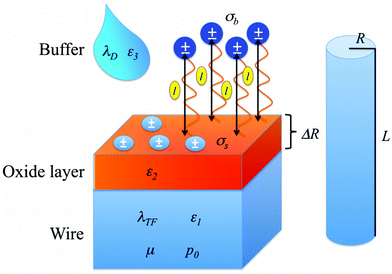
A nano-BIOFET sensor is a sensor based on a biomolecule binding another biomolecule that is linked to the surface of a nano-wire field effect transistor (FET).1–5 The resulting change in charge distribution affects the conductance of the FET, thus transducing the binding event. This is depicted in Fig. 1. The basic components of a nano-BIOFET are presented in Fig. 1a: a nano-wire, residing on an insulating oxide layer and back-gated, has a current flowing from the contacted source and drain electrodes. On the surface of the nano-wire, there is another oxide layer and a bio-functionalization layer. The bio-functionalization layer (Fig. 1b) is made of biomolecules linked on the surface of the oxide layer. These biomolecules can specifically bind a designated analyte (Fig. 1c). Before the binding, the charge carrier density inside the nano-wire is uniform (apart from defects or other unaccounted effects), and the current flow is constant (Fig. 1d). When the analyte is specifically recognized, it usually carries a charge close to the nano-wire surface, or more generally induces a change in charge in the bio-functionalization area. As depicted in Fig. 1e, a charge close to the nano-wire surface may cause a displacement of the charge carriers or an accumulation, depending on the sign of the charge. Thus, the current flow changes, a signal is generated, and the binding of the analyte can be recorded. The analyte biomolecules are carried by a buffer solution in which the nano-BIOFET is immersed. | ||
| Fig. 1 Pictorial representation of a generic nano-wire based BIOFET (not in scale). a) The different parts making up the device: a nano-wire resides on an insulating oxide layer through which is connected to the back-gate. Over the nano-wire there are the source (S) and drain (D) contacts, an oxide layer and the bio-functionalization layer. b) The device surface has been bio-functionalized, and a current is flowing through the nano-wire. The functionalization layer exposes to the buffer bio-molecules capable of specific molecular recognition. c) The specific analyte is recognized and adsorbed on the surface. The analyte carries a charge, or more generally induces a charge change in the functionalization area. This, in turn, induces a change in the current flowing through the nano-wire, which transduces the sensing event into an electrical signal. d) A p-type doped nano-wire: the positively charged holes are the charge carriers, responsible for the current flow. At equilibrium, the charge carrier density is (in theory) uniform and the current flow constant: base signal. e) If a positive charge approaches the nano-wire material, the charge carriers are displaced and the current flow diminishes. An approaching negative charge would create an increase in the current flow. Both situations generate a signal. | ||
Nano-BIOFETs are most appealing because of three main factors:
• Neither analyte nor receptor needs to be chemically labeled to allow for detection.
• The conductance sensitivity of nano-wires is very high, because it is inversely proportional to the radius of the wire.6 Nano-BIOFET sensors able to detect an analyte in the femtomolar concentration range have been reported.7,8
• The high binding selectivity often observed in biomolecules is incorporated in the sensor.
Most experimental studies on nano-BIOFET sensors have focused on a qualitative interpretation of the results, meaning a signal-change in the expected direction. For example, an increase in the conductance sensitivity in a p-doped nano-wire is observed after the binding of a negatively charged protein. Alternatively, a decrease in the conductance sensitivity is recorded due to a pH-induced charge decrease or an increase in Debye screening (increase of the ionic strength of the buffer solution). However, few studies have tried to quantify the change based on theoretical models by employing different levels of complexity for the description of the BIOFET devices.8–19 Some tools are also available on-line.14,18,20,21 Such quantification is needed to help guide the design of better nano-BIOFET sensors with known sensitivities. While there are many theoretical models aimed at rationalizing BIOFET signals, most experimental studies do not use them. Perhaps this is due to the complexity of the models and uncertainty on how to apply them in practical terms.
In this paper we present a computational methodology for predicting the change in conductance sensitivity  of a nano-BIOFET sensor. The methodology is a combination of the screening model of surface charge sensors in liquids (SMSCSL), developed by Sørensen, Mortensen and Brandbyge22 (summarized in section 2.2), with the PROPKA method (summarized in section 2.4.1) for predicting the pH-dependent charge of proteins and protein-ligand complexes, developed by Jensen and co-workers.23,24PROPKA is used to model the pH-dependent charge of a protein and accounts for the effect of the protein structure on the pKa values of the ionizable residues. The binding event is thus modeled as the binding of a single charge on the nano-wire, and thus presents the simplest possible theoretical model of a nano-BIOFET sensor. While other theoretical methods may be more accurate in the description of the physics of the nano-wires, our scope was to define and implement a simple model capable of being easily adapted to several different kinds of experiments with nano-BIOFET sensors.
The general aim of this paper is to attempt to define a methodology able to quantify (and possibly predict) the results obtained when employing nano-wire based BIOFETs. In particular, we combine the results of our simulations with the rationalization of published experimental results,25–27 in order to validate the predictions and gain a deeper insight into the different parameters that may affect the sensitivity of such devices. An emphasis is put upon the necessary knowledge and precision of such parameters, so that experiments performed with different nano-wires can be compared. In particular, we target a device built similar to those by the Lieber group.25
The paper is organized as follows: Section 2 gives the full description of the employed computational methods. Section 2.5 presents a typical nano-BIOFET setup (labeled GEN hereafter) and shows how the predicted conductance sensitivity changes while modifying each used parameter. This is done by quantifying the change in sensitivity upon a constant variation, in percentage, of the model parameters. In Sections 3.1–3.4, we apply the simulation model in order to reproduce four sets of published experimental data (EXP1-EXP4):
• Section 3.1 EXP1: The binding of avidin and streptavidin to a biotinylated nano-wire at pH 7.4.26
• Section 3.2 EXP2: The binding of avidin to a biotinylated nano-wire at pH 7.4, 9.0, and 10.5.26
• Section 3.3 EXP3: The binding of streptavidin to a biotinylated nano-wire in buffers of different ionic strengths corresponding to Debye screening lengths 0.7, 2.3, and 7.3 nm.27
• Section 3.4 EXP4: The binding of ATP to a ABL tyrosine kinase-functionalized nano-wire.25
Based on these results, a series of possible guidelines for the design of future nano-wire based BIOFETs is given in the Conclusions section.
2. Computational methodology
2.1 A screening model for nano-wire surface-charge sensors
In order to simulate the electrical response of a nano-BIOFET to a sensing event, we make some assumptions and approximations, in order to have the simplest possible model describing the phenomenon. We name this ensemble as the ‘single charge model’.In this model, the conductance change of a nano-wire is given by the equations defined by the screening model of surface charge sensors in liquids (SMSCSL) described in ref. 22 and 28. These equations will be quickly revised in section 2.2. The SMSCSL describes how the presence of charges close to the nano-wire influences its conductance. In our model, we assume that each molecule (protein or ligand) being sensed by the wire could be approximated by a single charge residing in the approximate center of mass of the molecule itself. The binding event is thus modeled as the binding of a single charge on the nano-wire. In the case of protein sensing, the charge depends on the pH of the buffer solution. In order to evaluate this charge, we employ the program PROPKA, ver. 2.0,23,24 as described in section 2.4.1. In the case of ligand sensing (ATP), the charge was fixed as −3 elementary charges.
The single charge was considered as distant from the wire surface as the considered protein would make it and surrounded by buffer solution. The presence of the buffer is considered by the usage of its ionic strength (as Debye length)29 in the equations of section 2.2. When evaluating the distance of the charge from the wire, the proteins were considered as directly residing on the surface of the wire oxide layer.
2.2 Theoretical background
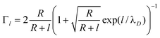
Following Sørensen et al.,22 the conductance change of a nano-wire due to a surface charge density directly on (σs), and at a distance l from (σb), the nanowire surface (Fig. 2) is given by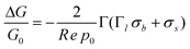 | (1) |
 | (2) |
 | (3) |
 | ||
| Fig. 2 Graphical representation of the various parameters involved in the definition of the single charge model. The nano-wire is a cylinder of radius R and length L, and is described by the parameters λTF, ε1, μ and p0. The wire is coated with an oxide layer of thickness ΔR and described by ε2. On the surface there are some charges, whose density is given by σs. On top of the wire, at a distance l there are some other charges, whose density is σb. These charges are immersed in a buffer solution, described by λD and ε3. | ||
| Parameter | Symbol | Value | (units) |
|---|---|---|---|
| Length | L | 2000.0 | (nm) |
| Radius | R | 10.0 | (nm) |
| Oxide layer thickness | ΔR | 2.0 | (nm) |
| Thomas–Fermi length | λTF | 2.04 | (nm) |
| Charge carrier density | p 0 | 1.11 × 1024 | (m−3) |
| Charge carrier mobility | μ | 0.01 | (m2 V−1s−1) |
| Wire permittivity (silicon) | ε1 | 12.0 | (ε0) |
| Oxide layer permittivity | ε2 | 3.9 | (ε0) |
| Solvent permittivity | ε3 | 78.0 | (ε0) |
The theoretical model includes two major assumptions regarding the charge concentration (e.g. p0 in eqn (1)): 1) they are assumed to be constant throughout the nano-wire and 2) they are not influenced by the electrostatic potential due to surface charges. More precise models of nano-wire conductance based on partial differential equations and homogenization have been published,15–17,31 and will be explored in future studies.
The screening in thin nano-wires close to the surface is markedly different from the bulk, and it remains an open question if this can be described in a simple way. On the one hand, a considerable deactivation of dopants can occur,32 while, on the other hand, the dopant concentration near the surface in nano-wires has been found to be orders of magnitudes higher than the bulk concentration33 and therefore could reach the degenerate limit. Here, we will simply employ a screening length to model this complex situation, which we denote λTF, although it is not clear to what extend the Thomas–Fermi model or the Debye–Hückel model will be able to describe the complex situation close to the surface. We will consider a doping level around 1–2 × 1018 cm−3 in which case both the Thomas–Fermi as well as the Debye–Hückel room-temperature screening lengths are close to 2 nm (see Table 1).
Another assumption is that the change in electrostatic potential due to the binding event can be adequately reproduced by a single charge.
2.3 Estimating parameters related to the nano-wire
In order to make all our results comparable with each other, we define here a standard nano-wire for all our determinations. We base our choice of parameters on the data reported by the Lieber group.34 We decide to simulate a cylindric nano-wire made of p-type doped silicon, with the characteristics reported in Table 1. The differences between our standard wire and those employed in the experiments, along with their possible consequences, are illustrated case by case in Section 3.1–3.4. By using the average values34 for the nano-wire radius, length, mobility and base transconductance, it is possible to retrieve an average value for the hole density p0 following eqn (4), inverse of Equation (13)†: | (4) |
In this way we can retrieve the average value for p0 reported in Table 1. The value for the Thomas–Fermi length is computed using the following equation:
 | (5) |
According to the parameters of Table 1, it is possible to estimate the base conductance G0 of our standard wire as 279.35 nS, following Equation (13).† In addition to these parameters, in order to be able to apply eqn (1), some other quantities have to be defined:
• the ionic strength of the buffer as Debye length λD in nm.
• the charge density of charges directly residing on the surface of the wire σs. In all present simulations we keep σs = 0 C m−2.36
• the charge density σb and distance l (in nm) of charges distant from the nano-wire.
The Debye length λD at which the experiments were conducted is evaluated using eqn (6) and (7):
 | (6) |
 | (7) |
2.4 Estimating parameters related to the nano-wire functionalization layer
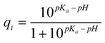
The charge density of the charges residing at a distance l from the wire surface can be defined as: | (8) |
Having defined (Section 2.3) the geometry of the nano-wire, one has to estimate the number N and the charge Q (in Coulomb) of the charges. In the case of proteins being sensed, their elementary charge has been estimated using the program PROPKA, as it is going to be illustrated in section 2.4.1. The estimation of the number of charges, instead, has been based on the dimensions and orientation of the protein systems involved, as will be described in Section 2.4.2.
 | (9) |
The overall charge of a protein is then simply given as a sum over the charges of the single amino acids: Q = ∑ qi. Note that the pKa value of an amino acid depends on the conformation of the protein. As shown in Fig. 4, the charge of a folded protein differs from its un-folded form.
Using the program VMD,41 we locate the center of mass of each apoprotein, center the protein structure on these coordinates and orient it along its main rotational axis. The minimum and maximum coordinate values along each axes are found, and assumed as the coordinates of the vertices of the parallelepiped enclosing the protein.
In our model, the charge being sensed is a point charge. When simulating the sensing of a protein, we locate such a point in the center of mass of the protein itself. In the case of a ligand, instead, we estimate an average distance between the ligand in the protein pocket and the surface upon which the protein is supposedly residing on the nano-wire surface.
2.5 Estimating the signal sensitivity
We devised the generic (GEN) setup as a plausible ensemble of parameters that should represent an average experimental setup. In particular, we choose to simulate the binding of a molecule carrying a −3 charge (e.g.ATP) in 5000 pockets at 2.0 nm from the wire surface, in the condition of a buffer Debye length of 2.0 nm. A standard nano-wire for all our determinations is defined in Table 1, based on the data reported by the Lieber group as described in Ref. 34.The generic setup GEN is used to assess the dependence of the signal sensitivity from the parameters of eqn (1). Inserting the data of the standard wire (Table 1) and GEN into eqn (1), one has a value for the conductance sensitivity  . While keeping the charge density value fixed (σb ≈ −1.366 × 10⁻³ C m−2), the parameters R, ΔR, ε1, ε2 and λD are varied singularly in 100 regular intervals in the range ±20% from the values of Table 1. For each parameter variation,
  is evaluated at each interval. The resulting total ensemble of values (ENS) is reported in Fig. 3a and 1Sa–d.† The value of the Thomas–Fermi length λTF is also similarly varied in a range ±20%, while still keeping the charge density values fixed (Fig. 3b), and
  evaluated at each interval.
 | ||
| Fig. 3 Signal sensitivity of the GEN setup with respect to various experimentally modifiable parameters of eqn (2), (1) and (3) of section 2.2. The conductance sensitivity of the simulated nano-wire is computed for 100 intervals in the range ±20% of the values of Table 1 for each parameter. In all calculations the charge density is kept fixed σb ≈ −1.366 × 10⁻² C m−2. a) The entire ENS is reported against the buffer Debye length λD. The majority of the ENS points are, logically, at λD = 2.0 nm and constitutes the vertical part of the graph. The points of ENS at λD = 1.6 or 2.4 nm show a lower or higher conductance sensitivity, respectively, than the rest of ENS. b) Sensitivity change against the Thomas–Fermi length λTF, in the range ±20% of the generic setup. Note the different scale on the y axis with respect to (a). At λTF = 2.04 nm, all ENS data points are included. Similar ensembles are computed at different values of λTF, namely 1.8, 2.2 and 2.4 nm. These results are also included in the graph. c) Relative sensitivity for the standard wire with 5000 charges with charge −3. The Debye length λD is fixed at 2.0 nm, while the distance between the charges and the wire surface is varied between 1.0 and 8.0 nm, that is, between 0.5 and 4 times the Debye length. The sensitivity values are reported as relative to the value at l = λD = 2.0 nm. | ||
The buffer ionic strength parameter has the most influence on the conductance sensitivity among the ENS data, as shown in Fig. 3a. The behavior is as expected: to a smaller value of λD corresponds a lower sensitivity.19,27,29,42 A ± 20% variation of λD from the value of Table 1 generates a ± 32% variation in the computed conductance sensitivity. A more ample spectrum of possible λD values is investigated in Fig. 2S.† While for smaller values (λD < 10 nm), the behavior is approximately linear as expected, the same is not true for larger values.
Another parameter involved in the description on the nano-wire is the charge carrier density of the wire. It could be varied by chemical or physical means, e.g. by varying the back-gate voltage. The charge carrier density of a p-type non-degenerate doped semiconductor can also be expressed as:
 | (10) |
The effect of the change in λTF is greatly more pronounced than with the other parameters previously considered, as can be noted by the different scale on the y axis. In fact, the sensitivity increases parabolically with the Thomas–Fermi length in a range far larger than what is found when considering the ENS data (−72% +180% variation). For a better understanding, all ENS data points are reported at the value λTF = 2.04 nm (vertical part). In this way, it is clear on which scale the parameters affect the nano-wire sensitivity. The effects of a larger Thomas–Fermi length on the sensitivity of a BIOFET device have been recently demonstrated.44 Additional evaluation of ENS data sets for different values of λTF (namely 1.8, 2.2 and 2.4 nm) are also reported in Fig. 3b. By increasing the value of the Thomas–Fermi length, the range of uncertainty on the sensitivity increases (ENS data have a larger span), while scanning the same range of values for R, ΔR, ε1, ε2 and λD. A BIOFET device based on a nano-wire with a large λTF would have a high sensitivity, but would require greater accuracy in determining the other parameters, in order for the results to be compared to those of other different devices.
Table 2 presents a qualitative summary of the response in conductance sensitivity of our standard device to a +20% change of the various considered parameters.
| Parameter | Conductance sensitivity change |
|---|---|
| a This parameter can be changed directly as part of the experimental set-up. b This parameter can be changed indirectly by modifying the charge carrier density through the back-gate voltage. | |
| Buffer Debye length λDa | + + + |
| Nano-wire radius Ra | − − |
| Nano-wire oxide layer thickness ΔRa | − − |
| Nano-wire permittivity ε1 | + |
| Oxide layer permittivity ε2 | + + |
| Nano-wire Thomas–Fermi length λTFb | + + + + |
An additional parameter that can be modified when designing a nano BIOFET is the distance l between the wire surface and where the charge giving rise to the signal can be located, e.g. by using molecules for the bio-functionalization layer of different sizes. In particular, the parameter l has to be considered in relationship with the Debye length λD. In fact, the more the sensed charge is distant from the wire surface, the more it is screened by the buffer solution. Fig. 3c presents the sensitivity response of the standard nano-wire (Table 1) and the GEN setup while keeping a fixed Debye length λD = 2 nm and varying the distance l between 1 and 8 nm, that is, between 0.5 and 4 times the Debye length.45 If considering the ideal situation l = λD as 100% of sensitivity, decreasing the distance l clearly induces a large increase in the computed conductance sensitivity. Once the distance between the sensed charge and the wire is half of the Debye length, the sensitivity of the device is ≈ 60% higher than the ideal situation. On the other hand, when increasing l, the sensitivity greatly diminishes. For example, once l = 4.0 nm, that is, twice the Debye length, the sensitivity of such a BIOFET device would be less than 36% of the ideal situation.
3. Results and discussion
Table 3 summarizes the different parameters characterizing each experiment discussed in this section. The retrieval of such parameters will be given in the next sub-sections.| Experiments | Experimental data [ref.] | What binds to what | Charge of what is bound, Q (elementary charges) | Charge density, σb/C m−2 | Charge distance, l/nm | Experimental buffer Debye length/nm | Experimental buffer pH |
|---|---|---|---|---|---|---|---|
| Experiment 1 | EXP1 [26] | Avidin to biotin | 16.18 | 5.114 × 10⁻² | 2.4 | 2.2 | 7.4 |
| Streptavidin to biotin | −8.49 | −3.578 × 10⁻² | 2.3 | 2.2 | 7.4 | ||
| Experiment 2 | EXP2 [26] | Avidin to biotin | 16.18 | 5.114 × 10⁻² | 2.4 | 2.2 | 7.4 |
| 12.65 | 3.998 × 10⁻² | 2.4 | 2.2 | 9.0 | |||
| −7.10 | −2.244 × 10⁻² | 2.4 | 2.2 | 10.5 | |||
| Experiment 3 | EXP3 [27] | Streptavidin to biotin | −8.49 | −3.578 × 10⁻² | 2.3 | 0.7, 2.3, 7.3 | 7.4 |
| Experiment 4 | EXP4 [25] | ATP to ABL tyrosine kinase | −3.0 | −3.623 × 10⁻³ | 2.4 | 131 | 7.5 |
3.1 Experiment 1: sensitivity of the binding of avidin and streptavidin
One aspect of the experiments by Stern et al.26 is being able to distinguish the binding of avidin or streptavidin to a biotinylated nano-wire. This mainly revolves around the different charges of the two proteins when in a buffer at physiological pH. In the work of Stern et al. a device made of p-type doped silicon was prepared in the shape of a bar with a trapezoidal cross section. Even if our standard cylindric wire is clearly different in shape, it should have a comparable behavior, even if not the same ‘surface to cross sectional area’ ratio. The nano-wires used by Stern et al. had an average mobility of 0.045 m2 V−1s−1 different from the one we employ (Table 1). Anyway, a different value of μ influences only the value of G0, not the sensitivity of a wire, as reported in the Computational Methods section. | ||
| Fig. 4 Charge-pH dependence curves for folded avidin (1AVD, continuous line) and streptavidin (1STP, continuous line) and unfolded forms (dashed lines), as based on the PROPKA result. Linear regression lines for the points at ±1 pH unit from the physiological pH of 7.4 (vertical dashed line) are also drawn as dashed lines. The slope of the line for avidin is −2.3, while for streptavidin is −3.9 (see also Fig. 11S† given as Supplementary Information). | ||
An analysis and a rationalization of the computed charge-pH curves for avidin and streptavidin are needed in order to be able to critically discuss the results based on the computed charges of the two proteins. The general shape of the titration curves of avidin and streptavidin is basically the same, the main difference being represented by the different pI points. Inside the range of the five pH units between the two pIs (5.16–10.18), the two proteins are oppositely charged. In the range of 1–2 pH units around the physiological pH (7.4) the slope of the two curves is less steep. This is more evident for avidin, while streptavidin maintains a relatively more steep profile. This is also depicted in Fig. 4.
At very low or very high pH, the two curves have reached a plateau: all ionizable amino acids have been protonated/deprotonated. The two proteins cannot reach a higher or lower overall charge than these plateau values. The only difference with the experimental data is in the pI values. This means, the experimental curves would possibly have shifted only left or right with respect to the curves of Fig. 4, following the difference of the pI values. In the next sections it will be shown how these factors (difference between computed and experimental pI, different slope around pH = 7.4) may influence the computed results.
It is interesting to note the difference between the predicted charge for folded and unfolded proteins. This difference is not constant, and it is more pronounced in the low pH regions. It is worth noticing that in both curves, the predicted isoelectric point for the folded state differs from the unfolded one by ca. 0.5 pH units. In the next sections, it will be shown how a small difference of only 0.5 pH units may influence the conductance sensitivity of a BIOFET device. This highlights how using charges computed based on the 3D structure, rather than the sequence, can increase the accuracy of nano-BIOFET modeling.
 upon binding of avidin or streptavidin to a biotinylated nano-wire. The computed values are relative to the standard wire with a p-type doping, while the experimental ones have been deduced from Fig. 3a (EXP1) of ref. 26. The last column reports the computed charge densities for the two protein setups.
| Protein | |I0|/nA | |I|/nA |
|
σb/C m−2 | |
|---|---|---|---|---|---|
| EXP1 | Avidin | 110.00 | 40.00 | −0.64 | — |
| Streptavidin | 140.00 | 295.00 | 1.11 | — | |
| Computed | Avidin | 557.46 | 19.51 | −0.97 | 5.114E−2 |
| Streptavidin | 557.46 | 977.79 | 0.70 | −3.578E−2 |

The coating of the wire with proteins is simulated as described in Section 2.4.2. The dimensions of the tetrameric structure of avidin46 are estimated as 64 Å wide, 66 Å long and 48 Å thick (see Fig. 12S†). The cavities for the recognition of biotin are located on the 64 × 66 faces, two pockets per face. Supposing that the wire surface would get completely saturated by avidin, it is possible to estimate the number of proteins on the standard wire as 3570. Since the tetrameric form of avidin is symmetric, its center of mass is at the center of the protein. For this reason we consider l = 48 Å ÷ 2 = 2.4 nm.
The dimensions of the tetrameric structure of streptavidin49 are estimated as 55 Å wide, 58 Å long and 46 Å thick (see Fig 13S†). The biotin molecules occupy two pockets on the 55 × 58 faces. Supposing again full coverage of the standard wire, it is possible to estimate the number of proteins as 4727. Also, since streptavidin in its tetrameric form is symmetric, we consider the center of mass of the protein as the middle of the protein, and consequently l = 46 Å ÷ 2 = 2.3 nm.
Inserting the computed values of the protein charges, together with the parameters reported in Section 2.4.2, into eqn (1) one obtains a ΔG value of −268.975 and 210.163 nS for avidin and streptavidin, respectively. Considering VSD = −2 V, one obtains the values reported in Table 4 as Computed.
Concordance is perfectly obtained between the computed signal and the sign of the protein charge. On the other hand, the computed and experimental signal sensitivities are not in concordance with respect to the ratio of their absolute values. We predict a higher signal sensitivity (in absolute value) for avidin, while experimentally the streptavidin signal has a higher sensitivity.
Following eqn (1), the value of the predicted sensitivity depends on the charge density σb, reported in the last column of Table 4. As shown in section 2.4, the charge density depends on the evaluation of both the surface coverage and charge of the two proteins. Since avidin and streptavidin have more or less the same dimensions, it is difficult to find what could differentiate the surface coverage of one protein from the other. Instead, in section 3.1.1 it has been noted how the charge–pH curves of the two proteins have different slopes around the value 7.4. Considering this fact, together with the possible left-right shifting of the curves, given the error on the evaluation of the pI points, could change the ratio between the computed charges of the two proteins, and consequently the charge densities and signal sensitivity. Still, one has to notice that a shift of +0.5 pH units would only give to avidin a charge of ≈ 15 and to streptavidin a charge of ≈ −11 elementary charges. This would, in turn, produce a predicted sensitivity of −0.88 and 0.91 for avidin and streptavidin, respectively. This change in sensitivity is not enough to account for the difference in ratio between the two proteins with respect to the experimental results.
Instead, the cause for the most part of the discrepancy has to be found, most likely, in the non-comparable nature of the nano-wires used in the experiments of Stern et al. Section 2.5 showed how differences in the construction parameters can affect the signal sensitivity, in particular the Thomas–Fermi length λTF. Another possibility is the non-linear response of the nano-wire conductance depending on operating point. Nevertheless, since there are not enough experimental values available, it is not possible to be conclusive on this respect.
3.2 Experiment 2: effects of pH change on avidin binding signal
In the same work, Stern et al. analyze the pH dependence of the signal generated when avidin binds to the biotinylated wire. As evidenced in Fig. 4, the charge of avidin depends on the pH of the surrounding buffer solution. By using the same apparatus as described in previous section, Stern et al. analyzed such dependence (EXP2, Table 3) and reported it in their Fig. 3c (see Fig. 4S†). While approaching the pH value corresponding to the isoelectric point, the overall charge of the protein constantly decreases. The nano-BIOFET signal generated by sensing avidin changes accordingly. This has been experimentally measured for pH values 7.4, 9.0 and 10.5, the last one being very close to the experimental pI value. Inserting in eqn (1) the pH dependent values of the protein charge results in the graph reported in Fig. 5. | ||
| Fig. 5 pH dependence of the normalized intensity |I/I0| upon binding of avidin on the biotinylated standard wire. The available experimental data as deduced from Fig. 3c of ref. 26 (EXP2) are also reported. | ||
To analyze our simulated data and compare them to the experimental one of EXP2, the following two aspects have to be taken in consideration:
1. Unfortunately, in EXP2 only the  values are reported. Equation (13)† is needed to reproduce these data, and this implies taking in consideration the different mobility values between the simulated and the experimental data. Considering this aspect means that the curve of Fig. 5 can be up–down shifted.
2. Another aspect is the difference between computed and experimental pI values for avidin, 10.18 and ca. 10.5, respectively. In addition, one has to note (Fig. 4) how the area around the isoelectric point is one of the steepest of the pH–charge curve. This means that a small difference in pH can cause a big difference in the protein charge. This is mostly evident in Fig. 5 for the values at pH = 10.5. While experimentally avidin should still have a positive charge, even if small, in our simulation it already has a not so small negative charge. This means that, as for the curves in Fig. 4, a right shift should be considered.
Considering the reasonable shifts of points 1 and 2, the concordance between experimental and simulated data is acceptable. The predicted signal change, in absolute value, between pH 7.4 and 9.0 is 0.19, while the experimental one is 0.30. The error on the signal change (≈ 36%) is smaller than on the signal itself: pH = 7.4, predicted 0.05, experimental 0.34, error ≈ 84%; pH = 9.0, predicted 0.25, experimental 0.64, error ≈ 62%. While our model is not able to predict with good enough accuracy the conductance sensitivity at a given pH value, we can affirm that it is able to reproduce the effects of a pH change on a signal by means of the charge of the sensed protein.
It is crucial to determine the signal–pH dependence if a protein is not only the sensed molecule, but the sensing agent for a nano-wire based BIOFET. In fact, one has always to consider the possible effects on the signal when changing solutions of, possibly, slightly different pH (false positives). In this respect, it is interesting to note how the change of signal (Fig. 5) follows the curvature of the pH–charge curve (Fig. 4). In other words, where the pH–charge curve is less steep, the change in signal is also less pronounced. It could then be desirable to design a BIOFET where proteins are used as sensing agents to capture a given molecule and the pH of the solution buffers used is, possibly, in a region where the protein charge does not change drastically with pH. In this way, small errors in the evaluation of the pH of the various buffers used during the experiment would not cause big changes in the recorded signal independent from the analyte contained in the buffer solutions themselves.
3.3 Experiment 3: effects of λD change on streptavidin binding signal sensitivity
In section 2.5 it has been shown how the ionic strength of a buffer solution influences the signal sensitivity (Fig. 3a). This has been experimentally studied by Reed and co-workers.27 In this work the authors used a nano-wire device in the shape of trapezoidal bar made of p-type doped silicon, similar to what described in section 3.1. The surface was biotinylated, and the signal generated by the adsorbance of streptavidin was registered at different Debye lengths, namely 0.7, 2.3 and 7.3 nm (EXP3, Table 3).We employed our standard wire, as described in previous sections. The protein charge (−8.49 elementary charges) was computed as in a buffer solution at pH 7.4. The resulting signal sensitivity (considering VSD = −2 V) against a change in ionic strength represented by λD is reported in Fig. 6. In the same figure, the experimental data as deduced from Fig. 2b of ref. 27 (see Fig 5S†) are reported as EXP3. In addition, the single value that was retrieved from ref. 26 (see Table 4) is also reported as EXP1.
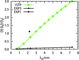 | ||
| Fig. 6 λD dependence of the signal change (|I|–|I0|) over the base signal |I0| when streptavidin binds to the biotinylated standard wire. The experimental curve (EXP3) is from available data as deduced from Fig. 2b of ref. 27. The single experimental point (EXP1) is deduced from Fig. 3a of ref. 26. | ||
The general trend of the curve made from our data is physically meaningful, and it resembles the experimental one. On the other hand, the values themselves are not really coincident with those of EXP3. It has to be noted, however, that the single experimental point from EXP1 is also not part of the curve of EXP3. It is important to remember the effects of the Thomas–Fermi length on the sensitivity of a wire. As seen in Fig. 3b, to slightly different values of λTF correspond large differences in signal sensitivity. The slope of the sensitivity against λD curve can change depending on the charge carrier density of the wire. By adjusting this parameter, it was possible to obtain the values of EXP1 and EXP3, for λD = 2.2/2.3 nm: λTF ≈ 2.21 nm gives, approximately, the value of EXP1, while λTF ≈ 1.31 nm gives, approximately, the value of EXP3.51
It is then possible to hypothesize that the response of a nano-wire to a change in the ionic strength of the analyte buffer is linear, except for values close to zero (see Fig. 7f†). On the other hand, the entity of such a response strongly depends on the Thomas–Fermi length of the nano-wire. In this respect, the devices used by the Reed group to perform EXP1 were, most likely, better performing than those employed in EXP3.
3.4 Experiment 4: ATP binding to ABL tyrosine kinase
As previously noted, probably the most interesting application for nano-wire based BIOFETs is the label-free recognition of small molecules as specific ligands of proteins linked to the nano-wire surface.Wang et al.25 report one label-free small molecule recognition experiment (EXP4, Table 3). In their experiments, they prepare a nano-BIOFET by linking Abelson (ABL) tyrosine kinase to a p-type silicon nano-wire, and then record the signal generated when adenosine triphosphate (ATP) molecules are adsorbed in the protein pocket. ABL is known to have a good affinity for ATP, with an experimentally estimated dissociation constant KD = 62 nM.52
We decided to reproduce such data, with particular reference to their Fig. 3b (see Fig 6S†). Wang et al.’s experiments are conducted using a buffer composed by 1.5 μM Hepes buffer at pH 7.5 containing 1 μM MgCl2 and 1 μM EGTA. In these conditions, following eqn (6) and (7) of section 2.3, it is possible to estimate the Debye length λD ≈ 131 nm.
In order to define the number and distance from the wire of the ATP charges, we estimate the number of cavities available for recognition. The crystal structure of ABL tyrosine kinase (2G1T)53 is approximated to a rectangular parallelepiped of approximate dimensions 40 × 50 × 60 Å (see Fig. 14S†). The ATP binding pocket is located on one of the 50 × 60 faces. In the experiments by Wang et al.,25 there is no mention of a mechanism acting towards the orientation of the protein on the wire surface. Considering an average over all possible faces and full coverage of the standard wire, it is possible to estimate that the number of proteins coating it is 5094. We suppose that ATP can be detected if and only if the protein surface linked to the wire is the one opposite to the face with the pocket. Considering the relative area of each face, it is possible to estimate the average number of available pockets is 1033 (ca. 20%). The distance from the wire of ATP once in the pocket can be estimated to be 2.4 nm, by manual repeated measurements when visualizing the pdb file.
The fraction of adsorbed ATP molecules with respect to the concentration in solution is computed following eqn (11).
 | (11) |
Considering the experimentally evaluated value KD = 62 nM, we obtain the saturation curve plot reported in Fig. 7. The complete numerical results are reported in Table 1S† as Supplementary Material. The curve shape is typical for adsorption phenomena, and compare well with the experimental one, reported in Fig 6S† and Fig 9S.† The order of magnitude of the curve is also in line. Our standard nano-wire has been, in fact, modeled on those used by the Lieber group. The chosen value for μ also assures this concordance.
 | ||
| Fig. 7 Computed signal dependence upon ATP concentration, following eqn (11) and the conditions described in Section 3.4. | ||
For a better understanding of the adsorption phenomenon we performed an analysis of the experimental data by various fitting, reported as Supplementary Information.†
With the knowledge of the experimental dissociation constant for a protein–ligand system, it is then possible to simulate the response of a nano-wire based device, where the protein is linked to the wire surface, based on the presence of the ligand in solution, possibly quantitatively too.
An analysis of the sensitivity dependence of the ABL-ATP setup, similar to what is presented in section 2.5, is reported as Supplementary Information in Fig7S.† In particular, it is interesting to note the exceptional value of λD used by Wang et al. At more usual values for Debye lengths, namely <5 nm, the nano-wire sensitivity is greatly reduced, and, for high ionic strengths, is basically zero. This can be seen in Fig 7Sf.†
4. Conclusions
In this paper we present a computational methodology for predicting the change in signal of a nano-BIOFET sensor (a sensor based on a biomolecule binding another biomolecule that is attached to a nano-wire field effect transistor (FET)) upon binding its target molecule. The methodology is a combination of the screening model of surface charge sensors in liquids (SMSCSL), developed by Sørensen, Mortensen and Brandbyge (eqn (1)),22 with the PROPKA method for predicting the pH-dependent charge of proteins and protein-ligand complexes, developed by Jensen and co-workers.23,24PROPKA is used to model the charge of a protein in its folded state, which serves as input to the SMSCSL model. The binding event is thus modeled as the binding of a single charge on the nano-wire, and thus presents the simplest possible theoretical model of a nano-BIOFET sensor. The methodology involves then the definition of the density and distance from the wire surface of such a charge. In addition, we define a set of parameters for a standard wire to be used in all our simulations.Our methodology is a first attempt to model the complete sensing process of a BIOFET in a self contained manner. This involves a description of the nano-wire physics and its response to approaching charges immersed in buffer solution, geometry and density of the bio-functionalization layer, charge and distance of the analyte molecules. Even if treated in the simplest possible way, all these different aspects require the knowledge of many parameters usually not reported in experimental papers. With this work, we would like to stress the need for reporting such extended data, in order to facilitate experiments rationalization.
The predicted change in conductance sensitivity based on this methodology is compared to previously published data on nano-BIOFET sensors obtained by other groups (summarized in Table 3). As noted before,54 reporting a sensitivity change instead of just changes in (relative) intensity would be helpful when comparing results obtained with different devices. Since, instead, all parameters necessary for the prediction are not always reported or known accurately, we also investigate how sensitive the predictions are to the individual parameters of eqn (2)–(3).55 Our findings can be summarized as follows:
• The SMSCSL predicted conductance sensitivity of a nano-BioFET is most sensitive to the Thomas–Fermi length (λTF) and, hence, the charge carrier density of the wire. While this has already been noticed for the conductance sensitivity of bare silicon nano-wires,22 it was not previously assessed for a model of a nano-wire based BIOFET. Fig. 3b shows that the increase in conductance sensitivity with increasing Thomas–Fermi length is approximately parabolic. A ±20% change with respect to the Thomas–Fermi length of 2.04 nm (Table 1) leads to a −72% to +181% variation in the predicted signal sensitivity, as shown in Fig. 3b. This has several important implications:
i) This sensitivity is the major obstacle to a quantitative prediction of the signal sensitivity, because a small uncertainty in the charge carrier density (to the extent that it is even reported for published BIOFET studies) can lead to a relatively big error in the prediction. For example, the discrepancy between the predicted dependence of the sensitivity on the ionic strength and that reported by Reed and co-workers (EXP3, Fig. 6) can be removed by changing the Thomas–Fermi length from 2.04 nm to 1.31 nm.
ii) Similarly, the sensitivity makes it difficult to compare results obtained for two different wires, since it is quite possible that they have even slightly different charge carrier densities. For example, the discrepancy between predicted and observed conductance sensitivity observed for EXP1 (Table 4) for avidin and streptavidin binding can be removed by changing the Thomas–Fermi length from 2.04 nm to 1.90 and 2.21 nm, respectively.
• After the Thomas–Fermi length, the SMSCSL predicted conductance sensitivity of a nano-BIOFET is most sensitive to the Debye length (λD) and, hence, the ionic strength of the solution surrounding the nano-BIOFET. Fig. 3a shows that the increase in conductance sensitivity with increasing Debye length is approximately linear, in the studied range. A ±20% change with respect to a Debye length of 2.0 nm (Table 1) leads to a ±32% variation in the predicted signal sensitivity—see also Fig. 6 for an example of experimentally evaluated dependence of the sensitivity from λD.
While the conductance sensitivity can be increased by lowering the ionic strength (longer Debye length), it should be kept in mind that many proteins become unstable at low ionic strength. Common buffers used in protein chemistry have ion concentration values of 6–23 mM, corresponding to Debye lengths of ca. 2–4 nm.
• The other parameters that enter the SMSCSL model have a smaller effect on the predicted conductance sensitivity (Fig. 1S†). A ±20% change with respect to the values listed in Table 1 leads to the following variations: −15%/+21% (wire radius), −15%/+13% (oxide layer permittivity), −7%/+5% (nano-wire permittivity) and −11%/+14% (oxide layer thickness), the most notable being R. A smaller radius corresponds to a higher sensitivity.6 However, it has been noted for silicon nano-wires that the noise-to-signal ratio increases while decreasing the cross-sectional area of the wire.56
• The conductance sensitivity varies linearly with the charge density (σb, eqn (1)). However, the charge density depends on several factors, such as the coverage of receptors on the surface, the concentration of analyte to be sensed, and in some cases the orientation of the receptor and pH. An evaluation of these factors would be needed in order to allow a comparison between different BIOFET devices, even if it might be experimentally challenging to achieve it.
• The parameter l (the distance of the sensed charge from the nano-wire surface) is also important, since both Γl (eqn (3)) and σb (eqn (8)) depends inversely from it. The ratio between l and λD has to be taken in consideration too, as it is clearly shown in Fig. 3c and relative discussion. The BIOFET linking agents should be designed to be as close as possible to the nano-wire surface in order to maximize the sensitivity of the device.42
We would like to stress that these results demonstrate the sensitivity of a BIOFET device to a ±20% uncertainty on one of the parameters. The effect of each parameter will depend on its absolute value. For example, an oxide layer 4 nm thick will have a significantly reduced sensitivity compared to a 2 nm thick layer, assuming all other parameters are identical.
Most nano-BioFET experiments to date add an excess of analyte, so that all available receptor sites bind a ligand. The underlying assumption is that the receptor-analyte binding constant is known, and unaffected by the presence of the wire. Similarly, a buffer pH is usually chosen to ensure as a large as possible charge for the analyte. If the analyte is a protein, it is important to note the charge can vary considerably with a small change in pH at certain pH values (Fig. 4). Thus, a small uncertainty in the pH can cause a relatively large uncertainty in the predicted conductance sensitivity.
In-so-far as the binding is saturated and the pH-dependent charge of the analyte is known precisely, the largest uncertainty in the predicted conductance sensitivity is the coverage of receptors on the nano-wire, which is rarely investigated and can be hard to estimate. Quantifying the coverage of active receptors is only really possible if the orientation of the receptors on the nano-wire is controlled, because the receptor-analyte binding usually occurs at a particular site, such as an enzyme active site. For example, in EXP4 (Section 2.4) the orientation of the receptor (ABL tyrosine kinase) on the nano-wire is not controlled, and it is therefore very difficult to estimate what coverage of the receptors can bind the analyte (ATP).
From a theoretical perspective, the two greatest limitations to the accuracy of the SMSCSL model are the use of the Thomas–Fermi model for the wire and a single charge for something as complex as a protein. The SMSCSL model is based on linear approximations and, consequently, the results only depend on the distance of the center of the charge distribution to the nano-wire. Thus, two molecules with different charge distributions but the same charge and center will yield the same result. This effect may contribute to the difference between computed and experimental sensitivities for avidin and streptavidin of Table 4. A more accurate model able to discern these cases is currently being studied by our group.
The SMSCSL model also ignores the fact that the wires are composed of semi-conducting materials with a significant band-gap and a charge distribution that may not be uniform (e.g. due to depletion at the surface or near the contacts). However, going beyond these simplifications may not be warranted until the key properties typical of current BIOFET experimental set-ups are known with greater precision.
Conversely, once the device characteristics of nano-wire BIOFETs can be controlled more efficiently, models such as the present one will be required for optimization of complex nano-scale biosensors.
The software package (BIOFET-SIM) written to predict the conductance sensitivity is open source (distributed under the GNU GPL) and can be obtained by contacting the authors. A web interface can be found at the address http://propka.ki.ku.dk/biofet-sim/.
Acknowledgements
Funding has been provided by the Danish Research Council for Technology and Production Sciences (FTP) and the Danish Natural Science Research Council (FNU). DMR is grateful to the Carlsbergfondet for the award of a fellowship. The authors acknowledge Nathalie Rieben and Yi-Chi Liu for fruitful discussions about the results.References
- M. J. Schöning and A. Poghossian, Electroanalysis, 2006, 18, 1893–1900 CrossRef CAS.
- M. W. Shinwari, M. J. Deen and D. Landheer, Microelectron. Reliab., 2007, 47, 2025–2057 CrossRef.
- D. Grieshaber, R. MacKenzie, J. Vörös and E. Reimhult, Sensors, 2008, 8, 1400–1458 CrossRef CAS.
- C.-S. Lee, S. K. Kim and M. Kim, Sensors, 2009, 9, 7111–7131 CrossRef CAS.
- S. Roy and Z. Gao, Nano Today, 2009, 4, 318–334 CrossRef.
- N. Elfström, R. Juhasz, I. Sychugov, T. Engfeldt, A. Eriksson Karlström and J. Linnros, Nano Lett., 2007, 7, 2608–2612 CrossRef.
- J.-i. Hahm and C. M. Lieber, Nano Lett., 2004, 4, 51–54 CrossRef CAS.
- P. R. Nair and M. A. Alam, Appl. Phys. Lett., 2006, 88, 233120 CrossRef.
- D. Landheer, G. Aers, W. R. McKinnon, M. J. Deen and J. C. Ranuarez, J. Appl. Phys., 2005, 98, 044701 CrossRef.
- D. Landheer, W. R. McKinnon, G. Aers, W. Jiang, M. J. Deen and M. W. Shinwari, IEEE Sens. J., 2007, 7, 1233–1242 CrossRef CAS.
- P. Nair and M. Alam, IEEE Trans. Electron Devices, 2007, 54, 3400–3408 CrossRef CAS.
- P. R. Nair and M. A. Alam, Nano Lett., 2008, 8, 1281–1285 CrossRef CAS.
- C. Heitzinger and G. Klimeck, J. Comput. Electron., 2007, 6, 387–390 Search PubMed.
- C. Heitzinger, R. Kennell, G. Klimeck, N. Mauser, M. McLennan and C. Ringhofer, J. Phys. Conf. Ser., 2008, 107, 012004 CrossRef.
- C. Ringhofer and C. Heitzinger, ECS Trans., 2008, 14, 11–19 Search PubMed.
- C. Heitzinger, N. J. Mauser, C. Ringhofer, Y. Liu and R. W. Dutton, Proc. Simulation of Semiconductor Processes and Devices (SISPAD 2009), San Diego, CA, USA, 2009, pp. 86–90 Search PubMed.
- C. Heitzinger, N. J. Mauser and C. Ringhofer, SIAM J. Appl. Math., 2010, 70, 1634–1654 CrossRef.
- S. Birner, C. Uhl, M. Bayer and P. Vogl, J. Phys. Conf. Ser., 2008, 107, 012002 CrossRef.
- Y. Liu and R. W. Dutton, J. Appl. Phys., 2009, 106, 014701 CrossRef.
- https://nanohub.org/resources/senstran .
- http://www.nextnano.de/nextnano3 .
- M. H. Sørensen, N. A. Mortensen and M. Brandbyge, Appl. Phys. Lett., 2007, 91, 102105 CrossRef.
- H. Li, A. D. Robertson and J. H. Jensen, Proteins: Struct., Funct., Bioinf., 2005, 61, 704–721 Search PubMed.
- D. C. Bas, D. M. Rogers and J. H. Jensen, Proteins: Struct., Funct., Bioinf., 2008, 73, 765–783 Search PubMed.
- W. U. Wang, C. Chen, K.-h. Lin, Y. Fang and C. M. Lieber, Proc. Natl. Acad. Sci. U. S. A., 2005, 102, 3208–3212 CrossRef CAS.
- E. Stern, J. F. Klemic, D. A. Routenberg, P. N. Wyrembak, D. B. Turner-Evans, A. D. Hamilton, D. A. LaVan, T. M. Fahmy and M. A. Reed, Nature, 2007, 445, 519–522 CrossRef CAS.
- E. Stern, R. Wagner, F. J. Sigworth, R. Breaker, T. M. Fahmy and M. A. Reed, Nano Lett., 2007, 7, 3405–3409 CrossRef CAS.
- M. H. Sørensen, Nanowires for chemical sensing in a liquid environment, 2007, Bachelor Thesis Search PubMed.
- J. N. Israelachvili, Intermolecular and surface forces, Academic Press, London, San Diego, 2nd edn, 1991 Search PubMed.
- F. W. J. Olver, Handbook of Mathematical Functions with Formulas, Graphs, and Mathematical Tables, Dover, 1973, pp. 355–436 Search PubMed.
- M. H. Sørensen, Nanowire Biosensor, 2009, Masters Thesis Search PubMed.
- M. T. Björk, H. Schmid, J. Knoch, H. Riel and W. Riess, Nat. Nanotechnol., 2009, 4, 103–107 CrossRef.
- E. C. Garnett, Y.-C. Tseng, D. R. Khanal, J. Wu, J. Bokor and P. Yang, Nat. Nanotechnol., 2009, 4, 311–314 CrossRef CAS.
- Y. Cui, Z. Zhong, D. Wang, W. U. Wang and C. M. Lieber, Nano Lett., 2003, 3, 149–152 CrossRef CAS.
- B. G. Yacobi, Semiconductors Materials An Introduction to Basic Principles, Kluver Academic Publisher, New York, 2003, p. 54 Search PubMed.
- In the presented model the effect of multiple charges on the conductance sensitivity is cumulative. The effects on the nano-wire conductance given by charges intrinsically residing on the nano-wire surface or carried by primary probes are considered as being part of the signal baseline. The reported changes in conductance (signals) are relative only to the charges of the sensed analytes.
- All quantities in eqn (6) are in SI units. Since, usually, concentrations are expressed in molarity, that is, mol L−1, the value of the ionic strength I has to be multiplied by 103 in order to be consistent: L−1 = dm−3 = 103 m−3.
- T. J. Dolinsky, J. E. Nielsen, J. A. McCammon and N. A. Baker, Nucleic Acids Res., 2004, 32, W665–667 CrossRef CAS.
- PROPKA 2.0 has a bug and it is not able to recognize all N+ terminal amino acids when multiple chains are present in a pdb file. This is the case for avidin (1AVD) and streptavidin (1STP), which constitutes four equivalent chains. To solve this problem, given the symmetry of the four chains, three additional N+ terminals, equivalent to the one already present, are manually added to the PROPKA output file, before evaluating the overall charge.
- For ASP, GLU, CYS, TYR and the C terminal the charge is computed as q′ = q − 1.
- W. Humphrey, A. Dalke and K. Schulten, J. Mol. Graphics, 1996, 14, 33–38 CrossRef.
- G.-J. Zhang, G. Zhang, J. H. Chua, R.-E. Chee, E. H. Wong, A. Agarwal, K. D. Buddharaju, N. Singh, Z. Gao and N. Balasubramanian, Nano Lett., 2008, 8, 1066–1070 CrossRef CAS.
- B. J. Van Zeghbroeck, Principles of Semiconductor Devices, http://ece-www.colorado.edu/%E2%88%BC; bart/book/, 2007, p. Sec. 2.6.4.3 Search PubMed.
- X. P. A. Gao, G. Zheng and C. M. Lieber, Nano Lett., 2010, 10, 547–552 CrossRef CAS.
- When increasing l and keeping the same number of sensed charges, the charge density σb decreases (eqn (8)). In other words, to the screening effect given by λD, there is the additional effect given by the direct dependence of the sensitivity on the charge density (eqn (1)).
- L. Pugliese, A. Coda, M. Malcovati and M. Bolognesi, J. Mol. Biol., 1993, 231, 698–710 CrossRef CAS.
- N. M. Green, Avidin-Biotin Technology, Academic Press, 1990, vol. 184, pp. 51–67 Search PubMed.
- D. Woolley and L. Longsworth, J. Biol. Chem., 1942, 142, 285–290 CAS.
- P. Weber, D. Ohlendorf, J. Wendoloski and F. Salemme, Science, 1989, 243, 85–88 CrossRef CAS.
- L. Chaiet and F. J. Wolf, Arch. Biochem. Biophys., 1964, 106, 1–5 CAS.
- The value of λTF we employed is based on average values reported in ref. 34, as described in section 2.3. By using the minimum and maximum values for the charge mobility reported in the same article, it was possible to compute the relative minimum and maximum values for the charge density using eqn (4) and λTF values of ca. 1.8 and 2.4 nm, respectively, using eqn (5). The values do not account for the effect of surface modifications and backgating (since the necessary information has not been provided in the literature). This data set is also not representative of all possible p-type Si based nano-wires, but represents just a plausible range.
- A. S. Corbin, E. Buchdunger, F. Pascal and B. J. Druker, J. Biol. Chem., 2002, 277, 32214–32219 CrossRef CAS.
- N. M. Levinson, O. Kuchment, K. Shen, M. A. Young, M. Koldobskiy, M. Karplus, P. A. Coe and J. Kuriyan, PLoS Biol., 2006, 4, e144 CrossRef.
- M. Curreli, R. Zhang, F. N. Ishikawa, H.-K. Chang, R. J. Cote, C. Zhou and M. E. Thompson, IEEE Trans. Nanotechnol., 2008, 7, 651–667 CrossRef.
- The absence of enough experimental data has prevented us from being consistent in presenting all our results as
 , when comparing with experiments.
 - S. Reza, G. Bosman, M. Islam, T. Kamins, S. Sharma and R. Williams, IEEE Trans. Nanotechnol., 2006, 5, 523–529 CrossRef.
Footnote |
| † Electronic supplementary information (ESI) available: Equation (12) and (13), Fig. 1S–Fig. 14S, and Table 1S. See DOI: 10.1039/c0nr00442a |
| This journal is © The Royal Society of Chemistry 2011 |