Polystyrene sphere-assisted one-dimensional nanostructure arrays: synthesis and applications
Liang
Li
*,
Tianyou
Zhai
,
Haibo
Zeng
*,
Xiaosheng
Fang
,
Yoshio
Bando
and
Dmitri
Golberg
International Center for Materials Nanoarchitectonics (MANA), National Institute for Materials Science (NIMS), Namiki 1-1, Tsukuba, Ibaraki 305-0044, Japan. E-mail: LI.Liang@nims.go.jp; liliang@issp.ac.cn; ZENG.Haibo@nims.go.jp
First published on 13th October 2010
Abstract
Polystyrene (PS) spheres can self-assemble into colloidal crystal monolayers that are currently employed for template-assisted synthesis of one-dimensional (nanopillars, nanorods, nanowires and nanotubes) nanostructure arrays. Compared to other classes of templates, PS-sphere monolayers can be easily formed and adjusted on substrates, and further manipulated using subsequent growth methods. Recently, several synthetic techniques have been developed and resulted in increased number of publications. Many applications including field-emitters, antireflection, light-emitting diodes (LEDs), photonic crystals, surface wetting, and photocatalysis have been reported utilizing these PS-sphere mediated nanoarrays. In this feature article, these synthetic strategies are highlighted along with a review of the applications emerging from current PS-sphere assisted nanoarrays and future challenges are analyzed.
 Liang Li | Liang Li was born in Anhui province, China, in 1979. He received his PhD degree from the Chinese Academy of Sciences and won the Excellent President Scholarship in 2006. After finishing JSPS research fellow in National Institute of Advanced Industrial Science and Technology (AIST), Japan, he joined Prof. Yoshio Bando's group in National Institute for Materials Science (NIMS) in Tsukuba, Japan. During these periods he has mainly focused on the fabrication, physical properties, and nanodevices of metal and semiconductor nanostructures. Particularly, he is developing various template techniques to fabricate nanostructured arrays. His current research is devoted to optoelectronic properties and applications in energy and environmental fields, including nanoscale photodetectors, solar cells, and lithium-ion batteries, etc. He has authored and co-authored about 50 refereed publications, which have generated over 600 citations. |
 Yoshio Bando | Yoshio Bando received his PhD degree from Osaka University in 1975 and joined the National Institute for Research in Inorganic Materials (at present NIMS) in the same year. From 1979 to 1981 he worked as a visiting researcher at Arizona State University. Currently, he is a Chief Operating Officer (COO) of the International Center for Materials Nanoarchitectonics (MANA) and a Fellow within the NIMS. He is also a visiting Professor at both Waseda University and the University of Tokyo. His current research concentrates on the synthesis and properties of various inorganic nanostructures and their TEM characterizations. He has published more than 450 papers and the total number of citations is over 11900. The H-index of his publications is 59. He also holds more than 150 patents. He received the 16th Tsukuba Prize in 2005 for his studies on novel inorganic nanotubes and nanothermometers. |
 Dmitri Golberg | Dmitri Golberg obtained his PhD degree from the Central Research Institute for Ferrous Metallurgy, Moscow, Russia, in 1990, and joined the NIMS, Tsukuba, Japan, 5 years later. To date, he has authored and co-authored more than 350 original papers and nearly 100 patents. His works have been cited over 7000 times. The H-index of his publications is 45. In 2005 he was awarded the 16th Tsukuba Prize for his studies on inorganic nanotubes using electron microscopy. He is currently a Group Leader and Principal Investigator within the MANA of NIMS, and an adjunct Professor of the University of Tsukuba. His current research focuses on the nanoscale material electrical and mechanical property studies in a transmission electron microscope. |
Introduction
Research on one-dimensional (1D) semiconductor nanostructures has become such an active field, since Wagner et al. reported the equation Rmin = [(2V)/(RTlns)]σ (R is the minimum whisker radius, V is the molar volume of the metal droplet, σ is the liquid–vapor surface energy, and s is the degree of supersaturation of the vapor) designed for nanowhisker growth.1 1D nanostructures including wires, rods, belts, tubes, and fibers,2–6 can be defined as those in which, the free mean path of charge carriers is larger than the available lengths in two spatial dimensions, therefore the carriers are confined only in one dimension. This confinement offers unique opportunities to control the density of state of semiconductors, and thus their electronic and optical properties. 1D nanostructures are considered as building blocks for the next generation of electronics, photonics, sensors, electrochemical, and energy applications.In the past few years, the synthesis of various 1D nanostructures such as metals, oxides, sulfides, nitrides, carbides, etc., has been addressed using numerous synthetic techniques, including vapor phase transport (vapor–solid (VS) and vapor–liquid–solid (VLS) processes), chemical vapor deposition (CVD), solution (solvothermal and hydrothermal) processes, pulsed laser deposition (PLD), template-assisted process, and so on.7–12 Unique applications in sensors, transistors, light-emitting diodes (LEDs), nanogenerators, batteries, and solar cells have been demonstrated.13–18 There exists a lot of published papers and reviews on the synthesis, properties, and applications of 1D nanostructures,19–22 therefore, this feature article will not treat these issues in detail.
The full potential of nanotechnology can be unleashed only when one is able to not only synthesize a wide range of nanoscale building blocks but also assemble them into various ordered patterns and in a controlled way. In particular, the application of 1D nanomaterials often requires their assembly in the forms of parallel or vertical arrays, on various conductive types of substrates for facile addressing, transport, contacts, and detection. For energy storage, ordered 1D arrays enhanced the capacity and rate capability in lithium-ion batteries, and light coupling and electron lifetime in dye-sensitized solar cells.23 For photonics, ordered nanowire arrays may constitute vertical high-refractive-index columns in air, making them natural candidates for two-dimensional (2D) photonic crystals.24 Introducing an array to LEDs has proved to be the most fruitful combination in integrated optics.25 For bio- and life-sciences, the pitch between pillars could influence cell adhesion.26 Although many unique applications utilizing such 1D arrays have fully been demonstrated, one of the contemporary challenges is still to assemble these ordered nanoarray structures so that they entirely realize their potential functionalities.
To accurately tailor 1D ordered arrays, nano-patterning techniques are required to have a capability to control their size, spacing, shape and orientation, and to allow high throughput, large area, and low costs. Up to now, many patterning methods have been developed for producing nanostructure arrays on substrates, including optical- or electron beam- lithographic methods, nanoimprinting, self-assembly, and template-assisted processes.27–31 Vertical nanowire arrays can also be fabricated by VLS and oxide-assisted processes.32,33 It is also worthy to note that Yang et al. reported the in situ fabrication and assembly of nanowire arrays on metal substrates.34 Among the patterning methods, template-based synthesis is the most commonly and widely used. The most commercially available templates are anodized alumina membranes (AAMs) and radiation track-etched polycarbonate membranes.35 Other membranes have also been used, such as radiation track-etched mica, silicon after electrochemical etching, mesoporous materials, zeolites, and existing nanostructures.36–40
Among the above methods, electron beam lithography (EBL) offers precise control over the size, spacing, and shape of nanostructures, but the process is complex involving the need to use resist materials, patterned areas are limited, throughput is low due to a long exposure time, and equipment costs are high. As one of various “hard” templates, AAMs have a good ability to produce complex 1D nanostructures and facile control in the composition, size and dimension. They can be combined easily with various synthetic techniques such as sol–gel synthesis, CVD, thermal decomposition, electrodeposition, atomic layer deposition (ALD), and so on. The diblock-copolymer process uses the interactions of two chemically distinct polymer chains to achieve ordered arrays with a size scale limited to chain lengths of the polymers. After the removal of one component polymer, an ordered porous nanostructure can be employed as a template. This template suffers from a poor control of spatial and size distribution, and it is only applicable to limited classes of materials. Existing nanostructures are also useful as templates to generate many 1D nanostructures that cannot be directly synthesized from raw materials, but it is difficult to achieve a tight control over the composition and reaction process. A common problem faced by hard templates is how to selectively remove templates after synthesis and keep uniform morphology after removal. In addition, nanostructures produced by template-directed methods are often polycrystalline, and the quantity of products in each run of synthesis is relatively limited.
Compared with “hard” templates, the so-called “soft templates” usually consist of organic surfactants, polymers, and even biological viruses, which are relatively flexible in shape. Similar to “hard” templates, the nanostructures obtained in these cases tend to be polycrystalline and may aggregate into bundles.
Recently, self-assembled colloidal crystal monolayers, composed of polystyrene (PS) spheres or silica, or PMMA, have attracted wide interest to fabricate the ordered arrays with well-defined micro/nanostructures because of their flexibility and controllable structure parameters.41–60 These templates are arranged with a hexagonal close-packed (hcp) or non-close packed (hncp) pattern on substrates, which could be directly used for wetting surfaces, Surface Enhanced Raman Scattering (SERS), and antireflective coating, photonic crystals, and so on.61–66 More importantly, they can also be used as flexible templates to fabricate 1D ordered nanostructure arrays. Since Deckman et al. prepared an ordered microcolumnar array using the PS sphere monolayer as a mask by the so-called natural lithography in 1982,67 this strategy has been well developed to synthesize 1D nanostructure arrays by different methods including reactive ion etching (RIE), electrochemical deposition, and CVD, using PS spheres as masks or catalysts, etc.68–71 The structures of 1D nano-arrays can be tuned by changing the diameter of PS spheres and experimental conditions. For example, Kuo et al. demonstrated the fabrication of Si nanopillar arrays with diameters as small as 40 nm and high aspect ratios up to ∼7. The size and shape of the nanopillars can be controlled by the size and shape of the sputtered aluminium mask, which are determined by the feature size of the PS sphere mask and the number of the colloid layers. Nanopillars with different shapes can also be fabricated by adjusting the RIE conditions such as gas species, bias voltage, and exposure period for an aluminium mask with a given shape.72 These 1D nanostructure arrays have a great variety of applications, especially in field emitters, photonic crystals, antireflection, wetting surface, and so on.73–77
This feature article is not intended to provide comprehensive information on 1D nanostructure arrays, rather, and it focuses on describing the status of research on 1D nanostructure arrays solely grown on PS sphere templates. After a brief introduction, the first section simply introduces the patterning technologies currently employed to synthesize PS sphere templates. In the second section, we address the recent progress in synthesizing 1D nanostructure (nanowires/nanorods/nanopillars/nanotubes) arrays based on PS sphere templates, utilizing various physical and chemical techniques such as RIE, CVD, electrochemical deposition, oblique angle deposition, etc. In the following section, the unique applications of these nanostructures in the fields of field-emitters, antireflection, LEDs, photonic crystals, wetting surface, photocatalysis, and so on, are described. Finally, the conclusions and outlook are presented.
Self-assembly of PS sphere templates
Many publications reported self-assembly strategies to form PS sphere templates on different substrates, which are not an emphasis in the present review. Here we mainly introduce the process describing previous modifications.78–86 Substrates (Si and glass) are pretreated in three steps: (1) ultrasonic washing in acetone, ethanol, and distilled water. (2) Subsequently immersing them in a mixed solution of H2SO4: 30% H2O2 (3![[thin space (1/6-em)]](https://www.rsc.org/images/entities/char_2009.gif) :1) at 80 °C for 1 h, and then keeping in the solution of H2O: NH4.OH: 30% H2O2 (5:1:1) to render the surface hydrophilic. (3) Washing with distilled water several times.
:1) at 80 °C for 1 h, and then keeping in the solution of H2O: NH4.OH: 30% H2O2 (5:1:1) to render the surface hydrophilic. (3) Washing with distilled water several times.
PS sphere monolayers were self-assembled on substrates by a spin coating process. Briefly, a droplet of PS suspension (2.5 wt.% in water, surfactant free) was dropped on the substrates fixed on a spin coater. The rotating speed was held at ∼1500 revolutions per minute (rpm) for 5 min and a PS monolayer with an area of about 2 cm2 was uniformly formed on the substrate by a self-assembly process. A typical scanning electron microscopy (SEM) image of a PS sphere monolayer is shown in Fig. 1.
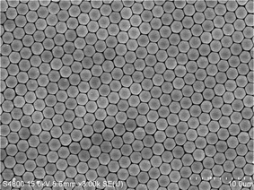 | ||
| Fig. 1 SEM image of a PS sphere monolayer on a Si substrate. | ||
Synthesis techniques
Self-assembled PS sphere colloidal crystals have been widely used as effective intermedium for the fabrication of 1D nanostructure arrays because they have several outstanding advantages Firstly, they can be facilely formed in a large area and with low cost. PS spheres can be readily self-assembled to single layers and multilayers with the hcp array (Fig. 1) under capillary forces arising from solvent evaporation.87–89 Several colloidal crystallization strategies have been well documented, including vertical deposition,90dip-coating,91spin-coating,92 nano-robotic manipulation,93etc. Although the process is very simple, the area of layers can readily reach cm2 and the hexagonal ordered degree is high. Secondly, this unique medium provides multi-scale and flexible tuning parameters. Besides the selection of a sphere size, PS spheres can be further tailored through many ways, such as annealing-induced deformation (Fig. 2)87,94 and plasma etching-driven non-closed packing (Fig. 3).95 Moreover, the final products of 1D nanostructure arrays can be further adjusted through the combination of colloidal crystal and subsequent growth methods, such as metal-catalytic CVD growth,71,85,96–105 wet or dry etching,68,106–113 solution growth,87,114–120 on-sphere deposition,76,77,121–123 and oblique angle deposition.124–128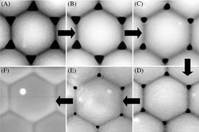 | ||
| Fig. 2 A 540 nm PS sphere latex mask annealed in 25 mL of water/EtOH/acetone mixture by (A) 1, (B) 2, (C) 4, (D) 6, (E) 7, and (F) 10 microwave pulses.94 | ||
 | ||
| Fig. 3 PS beads etched by O2 plasma with P = 150 W and V = 100 V. The etching times were: (a) 0 s, (b) 15 s, (c) 50 s, (d) 100 s, (e) 150 s and (f) 200 s.95 | ||
Metal dot-catalyzed CVD
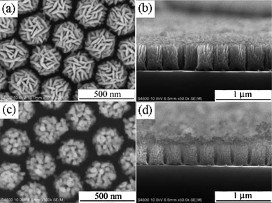
Generally, the pre-formed catalyst arrays on substrates can induce the CVD growth of semiconductor nanowires and carbon nanotubes. Good uniformity and high order of PS sphere colloidal crystals make them useful as templates to fabricate large-area ordered metal catalyst arrays. Combining PS template-directed metal arrays and CVD growth is a very effective method for the formation of 1D nanoarrays. Considering the self-assembled PS array and underlying substrate, there are two kinds of distinct surfaces. The first one is the interstices with an air–substrate interface, and another is the PS–substrate interface. Metal catalysts can be deposited on these surfaces, but the subsequent CVD-grown 1D nanoarrays have interesting differences.The fabrication process of 1D nanoarrays using the catalysts formed in the interstices is presented in Fig. 4a.96 Typically, after the self-assembly of PS nanospheres on a substrate, an Au film is deposited on the nanospheres. This usually forms a coating of Au on the upper part of the hemispheres, and a Au dot array on the substrates by penetrating a species beam through the interstices between the PS spheres. A pre-coating of PS nanospheres can narrow the holes between the spheres, and subsequently decrease the Au dot size. This is highly desirable for subsequent growth of single nanowires on individual Au dots. Fig. 4b presents the SEM image of well separated Au dot arrays grown in a large scale using this process. Fig. 4c shows the obtained ZnO nanowire arrays grown from these Au dots on a GaN substrate. It is clear that the nanowires possess a honeycomb lattice, the same as the initial Au nanodots. These nanowires exhibit high degree of ordering and are well separated (one wire from one dot). More commonly, the metal deposition on the pristine (without narrowing the holes) PS sphere monolayer prefers to form the inter-connected dot arrays, as shown in Fig. 4d.71 Moreover, the size of the metal dots is larger. As a result, the subsequent CVD growth produces the connected ZnO nanowire arrays, as shown in Fig. 4e.97 A honeycomb-like pattern is formed by these dense and well aligned ZnO nanowire arrays on the substrate, which can be used to fabricate photonic crystals, as presented below.
 | ||
| Fig. 4 (a) Schematic of a PS sphere interstices-metal dot-CVD process for making 1D nanoarrays. (b) Well separated Au dot arrays deposited in the PS sphere interstices and (c) subsequently CVD grown ZnO nanowire arrays.96 (d) Inter-connected Au dot arrays deposited in the PS sphere interstices and (e) subsequently CVD grown ZnO nanowire arrays.71,97 | ||
Some reports have demonstrated that the PS–substrate interfaces are also effective for the fabrication of catalyst arrays and can result in different 1D nanoarrays. According to Sie's strategy shown in Fig. 5a,98,99 a Au thin film is firstly ion-sputtered onto a clean sapphire substrate, and then the PS spheres are self-assembled on this substrate. The next important step is that the PS beads and the Au surface unoccupied by them are cleaned with oxygen plasma (Fig. 5b), and then the substrates are placed into the etching solution and developed. Fig. 5c presents the obtained Au particle hexagonal pattern. After the growth, highly ordered and uniform ZnO nanorod arrays are obtained, as shown in Fig. 5d and 5e. Obviously, this lithographic patterning method provides the site control for each nanorod. The arrays preserve the periodicity of the original PS sphere monolayer and have perfect ordering, uniformity, and surface facets.99
 | ||
| Fig. 5 (a) Schematic of a PS sphere interface-metal dot-CVD process for producing 1D nanoarrays.98 (b) A PS sphere self-assembled monolayer after a short time of O2 plasma etching. (c) The obtained pattern with Au particles formed on the PS-substrate interface. (d) and (e) ZnO nanowire arrays CVD-grown from this catalyst pattern.99 | ||
Furthermore, besides utilizing different parts of PS monolayer films, double layer PS self-assembled films and the relative alignment between these two layers can also be effective to adjust the metal dots and subsequent 1D nanoarrays.85 Usually, the metal nanoparticles deposited through PS monolayer have a quasi-triangular shape and hexagonal packing, which is determined by the aperture between the spheres in the mask. To overcome the restriction of triangular shape and the honeycomb lattice order, a double-layer masking is used. As shown in Fig. 6a, the first monolayer is self-assembled on the substrate by the conventional route, and the mask orientation is determined using a green laser pointer with the wavelength of 537 nm. Because all the used substrates are transparent, the diffraction patterns are clearly visible on the bottom of the preparation dish. Then, a second monolayer of PS is prepared in water. While the substrate with the first monolayer is fixed underwater, the second floating monolayer is moved right above the first masking layer and is rotated using tweezers. After e-beam evaporation, a honeycomb lattice of quasi-triangular metal particles can be obtained when a single mask is used, while a double-layer mask results in a triangular array of nearly spherical particles (Fig. 6b). Periodic nanoparticle arrangement in the arrays depends on the relative alignment angle between the two layers of PS. ZnO nanorods presented in Fig. 6c exhibit a very good correlation with arrays of catalyticNi nanoparticles. Therefore, each ZnO nanorod corresponds to a single Ni nanoparticle in the array.
 | ||
| Fig. 6 (a) Arrangement of the immersed first monolayer and the floating second monolayer with the schematic diffraction spots from the relative angles of 0° and 30°. (b) AFM image of particles resulted from a double-layer PS mask with a relative alignment angle of 10°. (c) SEM image of ZnO nanorods grown on Ni particles using a relative alignment angle of 7°.85 | ||
Besides the good controllability, the PS–metal dot-CVD method has another significant advantage. i.e. the flexible adaptability. Many kinds of 1D material arrays can be produced. Typically, in addition to the above-mentioned compound semiconductors, it can be applied to carbon nanotube104 and nanofiber105 arrays.
Selective etching
Besides the above bottom-up route, PS sphere monolayers can also play a significant role in the top-down fabrication of 1D nanostructure arrays. In such a route, the PS sphere monolayer usually acts as the mask for selective etching of thin films or bulk materials. According to the etching types, the PS sphere monolayer can be combined with wet etching through a solution chemical reaction106–110 or dry etching68,111–113 using RIE. In the former, the porous metal thin films are obtained through evaporation on the substrates covered with a PS monolayer, and then they play the catalytic function in the subsequent chemical etching process.106–110 In the latter, the PS monolayer or the PS-formed metal dot array acts as the shadowing mask for the direct ion etching formation of 1D nanoarrays.68,111–113For the chemical etching route assisted by the PS-formed metal films, the typical fabrication process is schematically illustrated in Fig. 7a.106 First, a monolayer of PS spheres is self-assembled on a Si substrate. Subsequently, the diameter of the PS spheres is slightly reduced by a RIE, which leads to the formation of colloidal particle arrays that are no longer close-packed. In the next step, a silver film is thermally evaporated onto the Si substrate as a catalyst. Owing to the PS monolayer mask, the Ag film is porous and has a hexagonal array of holes. Subsequently, an etching step is conducted in the mixture of deionized water, HF, and H2O2. The Ag film catalyzes the etching of Si beneath it. During the etching process, the “walls” of the honeycomb are gradually etched away and the remnant Si forms a nanowire array. Finally, the PS spheres are removed by dissolution in CHCl3, and the Ag film is dissolved in boiling aqua regia.
 | ||
| Fig. 7 (a) Schematic depiction of Si nanowire arrays through PS–metal-wet etching process. (b) and (c) Plane-view and titled-view SEM images of the formed Si nanowire arrays. (d)–(g) Cross-sectional images of Si nanowire arrays after wet etching for 4 min, 8 min, 12 min and 16 min.106 | ||
SEM images of the obtained Si nanowire arrays through chemical etching with the assistance of PS spheres are shown in Fig. 7b (plane-view) and Fig. 7c (titled-view). It is clear that the arrays are homogeneously distributed on the substrate over a large area. The mean diameter of the nanowires is 252 nm, matching well the corresponding value for the diameter-reduced spheres. A diameter of the Si nanowires can be controlled by selecting PS spheres with the desired diameter. Another parameter of the nanowire, the length, is related to the duration of etching process. Fig. 7d–g show cross-sectional SEM images of Si nanowires fabricated with etching times of 4, 8, 12, and 16 min, yielding nanowires with lengths of ca. 1.3, 2.7, 4.5, and 5.3 μm, respectively. The length of the nanowires varies linearly with the duration of the etching process, which provides good control over the length of the nanowire arrays. Interestingly, Si/Ge heterostructured nanowires can also be formed by the same procedure while using graded Si/Ge films as starting materials.108
Above wet etching is an isotropic etching technique; the profile can not be significantly changed after etching. Comparably, PS sphere-formed metal dot arrays can be used as masks for the controlled dry etching fabrication of Si 1D structure arrays through RIE.112 As shown in Fig. 8a, the triangular Ni dot arrays with a hexagonal order can be firstly fabricated through evaporation onto a PS monolayer-covered substrate. Varying the percentage of O2 in mixed etching gases, the size and morphology of Si nanopillars can be tuned (Fig. 8b). Fig. 8c and 8d show SEM images of Si nanopillar arrays fabricated with 25% and 12.5% O2 in the mixed etching gases of CF4 and O2. The corresponding nanopillars have heights and base widths of (270 nm, 220 nm) and (200 nm, 80 nm), respectively. The broader base widths of the nanopillars than the size of the mask is attributed to the shadowing effect of the mask during RIE and the change in oxygen fraction, hence the etching rate. The base width increases with the percentage of O2. The height/base width ratio shows a trend of decreasing with O2 content as its percentage reaches about 20%. The ability to control the size and shape of nanopillars with one size mask is attributed to the interplay of etching of Si and erosion of the Ni mask. Sharp tips and a flared base, which are advantageous for a high field emission current and mechanical/thermal stability, respectively, can be tailor-made depending on the applications.
 | ||
| Fig. 8 (a) SEM image of a Ni nanodot pattern after lift-off of PS nanospheres. (b) Schematic plots showing the variation of the slopes and base areas with the percentages of O2 in the mixed gas of O2 and CF4. (c) and (d) Triangular Si nanopillars fabricated by RIE with 25% and 12.5% O2 in the mixed gas of O2 and CF4.112 | ||
Besides the PS monolayer-formed metal dots, the PS monolayer can also be directly used as a mask for dry etching. Fig. 9 shows three major steps: spin coating of PS on Si, RIE with oxygen to tailor the size of the PS spheres, and deep RIE of Si to etch the pillar structure.68 In the second step, the diameters of the PS spheres are tailored by a parallel plate RIE etcher. In the third step, nanopillars are fabricated with diameter-reduced PS spheres on Si by applying the “Bosch” time-multiplexed RIE process.114–116 Since the bombardment of the reactive ions is directional and perpendicular to the surface of the substrate in the deep RIE etcher, the bottoms of the etched wells are preferentially etched during the etch phase of the etch cycle. The side walls are etched only minimally due to the parallel directionality of the reactive ions to the side walls and the protection of deposited polymers. Consequently, with appropriate etching masks and parameters, this etching process can produce Si structures with a high aspect ratio of up to ∼40 or more. The chosen etching process for the fabrication of small-size features is crucial over the ordinary RIE process. Such structures can be used for investigating the proof of principle in device architecture such as the vertical surround-gate FETs. Unlike other gas phase nanowire syntheses, this process does not require the patterning of a metal catalyst and thus minimizes the potential for unintentional wire doping.
 | ||
| Fig. 9 (a) Schematic diagram of Si nanopillar fabrication through PS-sphere dry etching. (b) SEM images of PS spheres-on-Si samples after the second and third step of the fabrication scheme, as shown in (a). Row A: top views of the PS spheres on Si substrates etched by oxygen plasma during 0–90 s. Row B and row C: top and side views of samples in row A etched by deep RIE. All scale bars are 750 nm.68 | ||
Solution growth
Recently, the combination of a PS sphere template with solution growth has received wide attention.87,117–120 Due to the low temperature during most of solution growths, the PS monolayer is facile in the process of electrochemical deposition,87,119 hydrothermal growth,117 and chemical deposition.118,120Electrodeposition is a very useful method for the nanowire growth within a large area. Furthermore, the deformation of a PS monolayer can be introduced to control the patterned nanorod arrays, as shown in Fig. 10a.87 Typically, a PS monolayer is self-assembled on a substrate through spin-coating, and then different degrees of template deformation are introduced under heating near the glass transition temperature. Finally, the electrochemical deposition is implemented on these deformed-PS monolayer covered substrates. Since the pattern of an array is confined by the shape and pattern vacancies within a template, the nanowire/nanorod density and uniformity of the formed arrays can be correspondingly adjusted. This benefits the improvement or their field emission performances.
 | ||
| Fig. 10 (a) Schematic of the fabrication based on the deformed colloidal monolayer templates and electrodeposition growth. (b) and (c) Continuous network and nanorod arrays obtained by short- and long-time growth from a pristine PS template. (d) and (e) Short and long nanorod arrays obtained by short- and long-time growth from the deformed PS template.87 | ||
The effects of template deformation are visible through the comparison of short time grown products by using PS monolayer templates without and with a heat treatment, as shown in Fig. 10b and 10d. When a standard template (without deformation) is used, only network-like pores or wall-like arrays can be obtained (Fig. 10b) after short time growth. By contrast, while utilizing a slightly deformed template, the growth of well-separated short nanorods (Fig. 10d) takes place due to the deformation-driven separation of voids within the template. If the deformation is excessive, some voids in the template fully vanish due to PS fusion, resulting in the absence of nanorods on these sites. For the arrays grown from the pristine template in Fig. 10c, the vertical nanorods stand in circles and are close to each other. When template heating time is increased to 1 min, the nanorod separation becomes obvious. The separation of nanorods is further developed with 1.5 min template heating in Fig. 10e. Such control coincides with the PS template evolution with heating. Such adjustment of local spacing is significant for the arrays' field emission performance when one considers the screening effect during electron emission. The method proposed here utilizes deformation-tailored colloidal monolayers and electrochemical deposition at temperatures as low as 70 °C without the needs of catalysts or preformed seed layers. The method is cheap and can be used to produce large-scale arrays.
Fig. 11 presents a recent example of fabricating nanotube-nanorod hybrid arrays using a PS monolayer.117Fig. 11a schematically describes the synthetic approach for making ZnO nanotube-nanorod hybrid arrays. First, a substrate such as glass or Si is coated with ZnO seed layers, followed by deposition of PS colloids. Then, a hydrothermal process is used to grow 1D ZnO nanostructures on the substrates patterned with PS colloid monolayers. This process results in the growth of ZnO tubular structures just below the PS colloids and solid nanorods at the apertures between three adjacent spheres.
 | ||
| Fig. 11 (a) A schematic illustrating the synthesis process for producing ZnO nanotube-nanorod hybrid structures with the use of PS colloid monolayers. (i) Deposition of a ZnO seed layer on the substrate by MOCVD. (ii) Fabrication of hexagonally close-packed PS colloid monolayer. (iii) Hydrothermal growth of ZnO nanostructures. (iv) Removal of PS colloids. (b) Schematic diagram of the proposed mechanism for the formation of single crystal ZnO nanotubes just below the PS colloids and increasing the length of solid nanorods enclosing the PS colloids.117 | ||
A formation mechanism of hybrid nanostructures is illustrated in Fig. 11b. Compared with the ZnO nanorod surfaces, PS colloid surfaces may provide more favorable sites for the decomposition of reactants into adatoms, and facilitate adatom diffusion. On the other hand, due to the capillary force, infiltration of precursors along the PS colloid surfaces can be stimulated. As a result, the growth rate of ZnO nanorods surrounding the PS colloids increases. The formation of nanotubes instead of nanorods just below the PS colloids revealed a marked change in the adatom transport due to the presence of the PS colloids. On the bare ZnO seed layers or around the PS colloids, solid ZnO nanorods form because the reactants or adatoms can get to the tips of the ZnO from above as well as from the side due to surface diffusion. However, PS colloids block the introduction of adatoms or reactants to the tips of ZnO crystals, therefore only the migration of adatoms along the surface of the PS colloids and ZnO sidewalls is allowed. As a result, a restricted supply of adatoms to the center of ZnO crystal tips causes the formation of tubular structures instead of solid nanorod structures.
On-sphere gas phase deposition
As mentioned above, utilizing the periodical spaces of the interstices among PS spheres or the periodical contact interfaces between PS spheres and substrates is typical for the growth or etching formation of 1D nanoarrays. Recently, an interesting strategy has been developed to apply the top parts of a PS monolayer to fabricate 1D nanoarrays with a hncp arrangement.76,77,121–123The fabrication process of hncp hierarchical TiO2 periodic nanorod arrays is illustrated in Fig. 12a.122PS monolayer colloidal crystals are firstly fabricated on cleaned Si substrates by spin coating. The substrate with a colloidal monolayer is then placed into the chamber for PLD in an off-axis configuration to the target. After PLD, the sample is put into an oven for heating in air. Fig. 12b and 12c present the SEM images of a sample produced by PLD at room temperature without further annealing. The sample demonstrates an ordered and well-structured array with a hcp arrangement. The cross-sectional image reveals that a TiO2 nanorod vertically protrudes from the corresponding PS sphere surface. The formation of a TiO2 nanorod array on a colloidal monolayer is attributed to multi-angle glancing angle deposition. When the structures were heated, the PS spheres were entirely burned out. At the same time, the TiO2 nanorods on the top of the PS spheres were changed to anatase polycrystals and moved vertically down to the original positions of the PS spheres. The volume of the TiO2 nanorod decreased during this process, and a hncp hierarchical nanorod array formed from the pre-existing hcp amorphous TiO2 array, as shown in Fig. 12d and 12e. The resultant film adhered tightly to the substrate after annealing. It could not be detached from a substrate even after ultrasonication in water. This guarantees its reliable application as a field emitter.
 | ||
| Fig. 12 (a) Schematic of the nanorod arrays fabrication on PS monolayer. (b) and (c) SEM image of an amorphous TiO2 hcp nanorod arrays on the colloidal monolayer before annealing. (d) and (e) SEM image of nanorod arrays on the colloidal monolayer after annealing in air.122 | ||
This method is very productive and can be applied to the formation of many other material 1D nanoarrays, such as hematite and Co3O4 hierarchical nanorod arrays.76,121 Furthermore, the morphology can be adjusted by the background pressure. Fig. 13 depicts SEM images of ordered hematite hierarchical columnar arrays deposited by PLD under different oxygen pressures at room temperature.121 These images illustrate that the target materials have been deposited on the top surfaces of each PS sphere and grown continuously along the vertical direction to form ordered columnar arrays, and the columnar arrays replicate the hcp arrangement of PS spheres. All the columns bear hierarchical structures that are composed of nanoplates at 6 Pa and nanoparticles at 60 Pa. After annealing, the columnar arrays have three characteristics that distinguish them from the as-deposited samples: (a) the arrangement of columnar arrays changes from the hcp to hncp form; (b) each column preserves its hierarchical structure, although the sizes of nanoplates and nanoparticles change slightly; (c) PS spheres disappear, and the columns are attached directly to the substrate.
 | ||
| Fig. 13 (a) and (b) SEM images of the hematite hierarchical columnar arrays PLD-synthesized on PS monolayer at an oxygen pressure of 6 Pa. (c) and (d) SEM images of arrays PLD-synthesized on PS monolayer at an oxygen pressure of 60 Pa.121 | ||
Shadowed oblique angle deposition
The oblique angle deposition (OAD) method is based on a conventional physical vapor deposition principle and can be used to fabricate aligned 1D nanostructure arrays.124–128 Typically, the surface normal of a substrate in the deposition chamber is positioned at a very large angle with respect to the incoming vapor direction, as shown in Fig. 14a.128 This deposition configuration results in a so-called geometric shadowing effect that leads to a preferential growth of nanorods on the substrate in the direction of deposition. The nanorods grow aligned but are tilted on large substrate areas.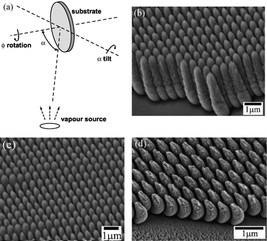 | ||
| Fig. 14 (a) Schematic of oblique angle deposition.128 (b) Side-view and (c) top-view of Si nanopillars by PS sphere-shadowed OAD. (d) Cr nano-half-moons.124 | ||
OAD on flat substrates involves a stochastic nucleation process yielding layers consisting of randomly distributed columns. In contrast, periodic arrays are achieved by substrate patterning prior to deposition, such as covering with a PS monolayer.124 In this case, the patterned surface mounds are the nucleation sites for the OAD columns, since atomic shadowing of the deposition flux suppresses growth on the surrounding substrate.
Fig. 14b-14d show SEM micrographs of regular arrays of nanopillar structures grown on substrates patterned using 500 nm-diameter PS spheres.124Fig. 14b and 14c are cross-sectional and plan-view micrographs of a Si nanopillar array grown from a constant angle of 72° with respect to the surface normal without polar substrate rotation. The pillars are tilted towards the direction of the incoming deposition flux, which impinges on the substrate from the left back. The front of the image shows an area of the substrate with no microspheres, corresponding to an extended patterning defect. This area exhibits no layer growth since the substrate is shadowed during deposition, first by the array of microspheres and then by the growing Si nanopillars. The Si nanopillars perfectly replicate the close-packed arrangement of the underlying microspheres. Fig. 14d shows an array of Cr nano-half-moons on 500 nm PS microspheres grown from an angle of 86° with respect to the surface normal. The half-moons are 300 nm wide and represent well-separated nanostructures. Therefore, the PS sphere-assisted process improves the OAD technique from the random growth to the ordered patterns.
Applications of PS-sphere assisted 1D nanoarrays
PS-sphere assisted 1D nanostructure arrays have been used in a large number of applications. Controlled size, height, periodicity, morphology, and shape have made them good candidate materials for use in field emitters, wetting surface, antireflection, photonic crystals, light-emitting diodes, and photocatalysis, and so on. In the following section we briefly review these applications utilizing PS-sphere assisted 1D nanostructure arrays.Field emitters
Field-emission is a form of quantum tunneling in which electrons overcome the work function that binds them on the surface of an emitting material to the anode in the presence of a high electric field. The field emitters can find wide applications including flat panel displays and high-powered vacuum electronic devices.129 The performance of field emitters is highly dependent on the intrinsic property (work function) and the shape of cathode material. The emission current density (J) produced by a given electric field (E) is described by the Fowler–Nordheim (FN) equation:130–133| J = (Aβ2E2/ϕ)exp(–Bϕ3/2/βE) | (1) |
Here A = 1.54 ×10⁻⁶ A eV V−2, B = 6.83 × 10³eV−3/2 V μm−1; ϕ is the work function of the emitting material, it has a fixed value for a particular material; β is the field-enhancement factor, which is related to the geometry, crystal structure, and spatial distribution of emitting centers. β can be expressed as β = h/r, where h is the height and r is the radius of curvature of an emitting center. Thus, materials with higher aspect ratios and sharper edges produce higher field-emission currents. Since the discovery of carbon nanotubes, much attention has been paid to exploring the prospects of 1D semiconductor nanostructures as field-emitters due to their low work functions, high aspect ratios, and high mechanical stability, etc.134–138
Among 1D nanostructures, the periodic and sharp (tapered) nanorod arrays are very useful for producing a low turn-on voltage and a fairly stable emission current due to the elimination of the shield effect on densely packed nanostructure arrays. Recently, our group reported that the density and tapering of ZnO nanorod arrays had effectively been controlled and their field-emission properties optimized by tuning the size and heating-induced deformation degree of PS templates.87 As the heating time was fixed, the turn-on fields (a field required to produce an emission current density of 0.1 mA/cm2) first decreased sharply from 12 V/μm to 2.4 V/μm with a diameter of PS spheres decreasing from 1000 nm to 500 nm, and then slightly increased under further diameter decrease, as shown in Fig. 15a. Large-diameter PS spheres produced a low nanorod density, which led to an insufficient number of the emitting sites and depressed the emitting efficiency, and small-diameter PS spheres largely increased the density and thus the screening effect appeared, which increased turn-on field again. With increasing the heating time of templates, the turn-on field firstly decreases and then dramatically increases (Fig. 15b). The nanorod separation can be improved by a slight deformation of the template applying a short heating time, which decreases the screening effects and increases the emitting efficiency. However, the excessive heating induced the absence and bundling of nanorods in some places. The former reduced the overall density of the array, and the latter increased the local screening effect, both reducing the emitting efficiency. Such controlled high performance has also been implemented in TiO2 nanorod arrays fabricated by a PLD process, in which the TiO2 nanorod arrays with the smallest periodicity and the largest distance between adjacent nanorods exhibited the best field-emission properties.
 | ||
| Fig. 15 J–E curves of ZnO nanorod array anodes grown from PS templates with (a) different PS diameters and (b) different heating times.87 (c) The height of Si nanopillars and width of the base as a function of the percentage of O2 in the etching gas and corresponding J–E relationships (d). The inset shows a ln(J/E2)–1/E plot.112 | ||
The advantages of sharp structures for improving field-emission properties were demonstrated by Chen et al.112Fig. 15c shows that the slope and aspect ratio of triangular Si nanopillars are controlled by variation of the mixing ratio of CF4 and O2 in the PS sphere template-assisted etching process. High field-enhancement factor (4184) and low turn-on field (1.6 V/μm at a current density 0.1 μA/cm2), as shown in Fig. 15d, were attributed to the high density, sharp tips, and well-controlled spacing between nanopillars, so that the shielding effect was minimized. Compared to nanorods with uniform diameters, nanorods with shaper tips must show more promising applications in the field-emission field.
Wetting surface
The wetting (hydrophobic or hydrophilic) conditions of a solid surface, depending on its inherent chemical nature and surface geometry microstructure, can find important applications in various fields, such as self-cleaning, antifogging coatings, microfluidics, and manipulation of biomolecules.139–143 Superhydrophobic surfaces with the contact angles (CAs) larger than 150° can be obtained by enhancing the roughness of hydrophobic surfaces (CAs larger than 90°) or by modifying rough surfaces with low free energy materials, usually composed of fluorine or silicon. Superhydrophilic surfaces (CAs less than 10°) can be realized through a two- or three-dimensional capillary effect on hydrophilic surfaces (CAs less than 90°), while applying UV irradiation. To these aims, a variety of fabrication and surface-modification strategies including CVD, lithographic patterning, plasma etching, and wet-chemical grafting, have been exploited to obtain artificial wetting surfaces.123,144–151 A challenging direction in this research field deals with the fabrication of superhydrophilic surfaces of semiconductor metal oxides without UV irradiation.PLD has proven to be an effective method to obtain superhydrophilic surfaces of metal oxides (TiO2, Co3O4, and Fe2O3) without UV irradiation.76,121,123Li and co-workers reported the controllable superhydrophilicity without UV irradiation in ordered and aligned Co3O4 hierarchical nanorod arrays obtained by PLD on PS sphere monolayers.76 The contact angles can be adjusted by controlling the background oxygen pressures during PLD and the post-annealing temperatures in air (Fig. 16a). Upon chemical modification with low-surface-energy fluorosilane, the superhydrophilic surfaces (Fig. 16b) were transformed into superhydrophobic ones (Fig. 16c). The authors attributed these phenomena to the improved roughness of the hierarchical structures and the abundant OH−groups induced by the PLD and subsequent annealing processes. Further work in this area will focus on fabricating other metal oxide nanostructures such those made of ZnO2, SnO2, and WO3, and exploring the generality of superhydrophilicity utilizing such a PLD process.
 | ||
| Fig. 16 (a) Contact angles of water on the surface of Co3O4 nanorod arrays deposited using different gas pressures and deposition times. Optical photographs of the water droplet shape on the surface of Co3O4 nanorod array made viaPLD in oxygen at 93.1 Pa (b) and after the fluorosilane surface modification (c).76 | ||
Light-emitting diodes
Nitride-based LEDs have been widely used for various applications, such as traffic signals, full color displays, and illumination lighting by white LEDs.152 LEDs with high external efficiency are highly demanding for the applications. The total light external efficiency of LEDs is a product of the light internal efficiency and the light extraction efficiency.153,154 However, the internal quantum efficiency is usually reduced by the high threading dislocation densities, owing to the large lattice mismatch and thermal expansion between the epitaxial GaN film and sapphire substrate. Moreover, the light extraction efficiency of a LED is limited by the critical angle loss, which is due to the large difference in refractive indexes of the epitaxial film (2.5) and the surrounding air (1.0). To diminish these negative factors, PS sphere template-assisted technology was applied to incorporate the nanoscale features into the LED structures and to enhance the light external efficiency. Three typical processes are shown in the following paragraph.(1) Patterned sapphire substrates (Fig. 17a and 17b).155Nitride-based LEDs were grown with different pattern sizes on patterned sapphire substrates by using conventional photolithography and PS sphere templates. The structural and leakage current measurements indicated the crystalline quality of epitaxial GaN film could be effectively improved by using the PS sphere template technique and the threading dislocation densities were decreased, which improved the internal quantum efficiency. The pattern size was related to the capability of light extraction, namely, the smaller pattern size could increase the number of patterns for the same area of the sapphire substrate, and thus increased the possibility of light scattering, which induced the high light extraction efficiency and the high output power. (2) Nanopillar top contact layers (Fig. 17c and 17d).156 A nanopillar patterned indium-tin-oxide (ITO) top contact layer was introduced into a LED structure by using size-tunable PS spheres as templates. It was found that the light output power (at 20 mA) of the LEDs was enhanced by 10%, compared with the conventional LEDs due to an increase of the extraction probability of the internally reflected photons through the patterns. (3) Nanoscale textured sidewalls (Fig. 17e and 17f).157 Apart from the above two strategies of multiple scattering from a rough surface, Huang et al. investigated the nitride-based LEDs with nanoscale textured chip walls fabricated using PS sphere templates and dry etching techniques. The LEDs with textured sidewalls increased the output power of the InGaN-GaN multiple quantum well LEDs by a factor of 1.3, indicating that the LEDs with nanoscale textured sidewalls had the larger light extraction efficiency. The output/input power efficiency was 30% higher than for the conventional LEDs due to the enhanced light output power.
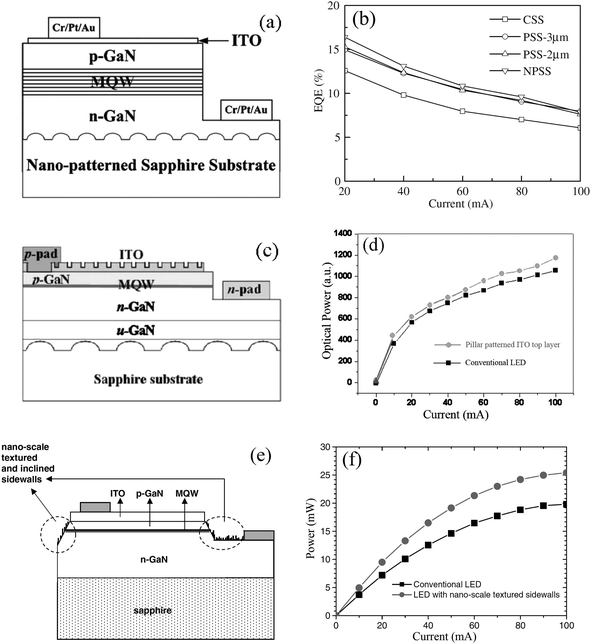 | ||
| Fig. 17 Schematic diagrams of LED structures (a) grown on a nanosphere-patterned sapphire substrate (NPSS),155 (c) with a pillar patterned ITO contact layer,156 and (e) with nanorod-textured sidewalls.157 Corresponding (b) external quantum efficiencies, and (d) and (f) light output power, respectively. | ||
Antireflection
A broadband antireflection property has been of prime interest for various applications. It may enhance the efficiency and sensitivity of optoelectronic devices such as solar cells, light emitting diodes, and photodetectors.158,159 For example, the high reflective index of Si results in up to 40% of the incident light being reflected, which severely limits the performance of Si-based optical and optoelectronic devices. Film coatings with intermediate or gradient refractive indices are usually utilized to suppress undesired reflection. Unfortunately, these techniques meet some troubles with respect to the production cost, duration, and reliability. Since the antireflection was discovered on the corneas of nocturnal moth eyes,160nanostructure arrays with the dimensions smaller than the wavelength of incident light have been studied as an alternative.161–163 This way is more stable and durable than surface coatings since only one material is involved.Several groups have developed a facile PS sphere template-assisted process to create antireflective Si nanopillar/nanorod arrays. The Si nanoarrays exhibited broadband antireflections, and the spectral positions with low reflection strongly depended on the periods of these arrays. For instance, the low reflection (8%) range of a 300 nm Si array is 500–1100 nm, but it becomes 900–2400 nm on the 1.1 μm Si array.164 Thus, the wavelength range of low reflection can be tuned by varying the periodicity of an Si array, which can be controlled by the sizes of PS spheres. Studies on other antireflective nanostructures such as carbon nanotube arrays have also begun in regard of the hopes to theoretically understand the mechanism of ultralow reflection.165
Photonic crystals
Photonic crystals are ordered nanostructures in which two media with different dielectric constants or refractive indices are arranged in a periodic form.166 The periodic structures can be used to control light propagation in a way analogous to semiconductor lattices with electrons. 2D photonic crystals have attracted much interest due to the relative ease of achieving a full photonic band gap.167,168 Generally, 2D photonic crystals have been fabricated by a top-down process, i.e.electron-beam lithography, which is expensive and has a low throughput.169 Recently, by using PS spheres to define a catalyst pattern, 2D periodic arrays, such as ZnO nanorods and their networks, and carbon nanotubes, have been fabricated and utilized as 2D photonic crystals. This approach is relatively simple, cost-effective, and has a high throughput.Wang et al. fabricated 2D photonic crystal slabs starting with PS sphere patterned ZnO nanorod arrays that were conformally coated with TiO2 by atomic layer deposition.97 This periodic structure showed a reflection peak (2670 nm) close to the theoretically predicted bandgap region between 2440 to 2243 nm, as shown in Fig. 18a. The bandgap can be controlled by varying the period of a PS sphere template, which is feasible down to ∼100 nm; thus, a 2D photonic crystal with a bandgap in the visible light region can be expected. To achieve a visible bandgap, Chen's group firstly designed 2D nanorod network photonic crystals with a bandgap in the green light emission region, which were fabricated by an aqueous chemical method with PS spheres as templates.170 A peak at 437 nm in the reflection spectrum was in an excellent agreement with the calculated photonic crystal band gap region from 458 to 434 nm (Fig. 18b and 18c). These interesting results undoubtedly push forward potential applications of PS spheres, but it is still a challenge for this technique to fabricate structure-adjusted photonic crystals with various bandgaps, particularly in the visible range.
 | ||
| Fig. 18 (a) Left: Reflection spectrum of a TiO2/ZnO quasi-2D photonic crystal slab after the reference is removed. Right: Calculated photonic band structure.97 (b) Calculated photonic band structure of the 2D ZnO nanorod networks and corresponding reflection spectrum (c) measured at the 85° incident angle.170 | ||
Photocatalysis
As global population growth and economic development continue to ramp up, sustainable energy production and environment are emerging top issues and challenges for humanity. Photocatalysis is an important chemical process that underpins the development of critical renewable energy and environmental technologies such as photocatalytic water/air purification, hydrogen production from splitting water, and high-efficiency/low-cost solar cells.171–173 In 1972, Fujishima et al. achieved an UV light induced water dissosiation using a TiO2 photoanode in combination with a platinum counter electrode soaked in an electrolyte aqueous solution.174 Since then, semiconductor photocatalysis has attracted considerable attention.175–178 A general mechanism based on the electron paramagnetic resonance (ESR) and laser flash photolysis measurements, taking anatase TiO2 (band gap of 3.2 eV) as a typical example, has been proposed by Hoffmann and co-workers,179 as shown in Fig. 19a. This mechanism includes four primary processes, namely, charge-carrier generation, trapping, recombination, and an interfacial transfer. When a photon with an energy of hν matches or exceeds the band gap energy (Eg) of the semiconductor, an electron in the valence band (VB) is excited into the conduction band (CB), leaving a positive hole (h+) in the VB. The photogenerated electrons and holes can initiate redox reactions with chemical species adsorbed on the surface or interface of the photocatalysts. The detailed mechanism of the TiO2 photochemical reaction has been well-documented.180,181 | ||
| Fig. 19 (a) Photoexcitation of a semiconductor (e.g., TiO2) and the subsequent generation of an electron and a hole, which are trapped by an oxidant (Ox) and a reductant (Red), respectively. For TiO2 photocatalysis, the “Ox” is a surface-adsorbed oxygen molecule, and the “Red” is a surface-bound hydroxyl group.175 (b) Photocatalytic activity evaluation of different substrates based on the absorbance ratio A/A0 as a function of UV irradiation time. A and A0 are the absorbance after the UV irradiation and that from the initial surface, respectively.77 | ||
Photocatalytic processes are influenced strongly by the phase, shape, size, doping, crystallinity, and surface area of photocatalysts.182–184 Recently, Liet al. fabricated a hexagonal-close-packed, hierarchical amorphous TiO2 nanocolumn array by PLD using a PS monolayer as a template.77 Compared with the amorphous film and the anatase nanocolumn arrays, the amorphous nanocolumn arrays demonstrated the best degradation performance for stearic acid (Fig. 19b). Anatase is usually deemed to be more photocatalytically active than the rutile and amorphous TiO2. However, these results fully imply that in addition to the crystal phase, other factors, including the specific surface area, crystal composition, and material microstructures, also significantly affect the photocatalytic performance. In their report, the amorphous nanocolumn array had porous structures and possessed a much higher specific surface area than that of an anatase nanocolumn array, which contributed to better photocatalytic properties. This suggests that the surface area of TiO2 prevails over its crystal structure with respect to enhancing a photocatalytic activity. In addition, the enhanced photocatalytic activity of amorphous TiO2 nanocolumn arrays compared with amorphous films was ascribed to special hierarchical structures composed of radiation-shaped nanobranches emanating from a center point on the PS sphere. Such advantages of hierarchical nanostructures were also confirmed in a Fe2O3 photocatalytic system.121 The role of surface states, particularly the oxygen vacancies/defects, in improving photocatalytic efficiency needs further investigation, because the authors also found the effect of these oxygen vacancies/defects on surface wetting behaviors.
Others
One objective of bio-interfaces is to control the conformation and activity of the immobilized biomolecules in order to perform parallel biochemical analysis or to culture cells by maintaining their phenotypes. Micro-patterning operations are often performed to control the size, location, and geometry of patches where biomolecules or cells are immobilized. Valsesia et al. reported that the combination of PS spheres and plasma deposited functional polymeric layers can fabricate chemically nano-patterned surfaces with biologically relevant end groups such as carboxylic groups or antifouling PEO-like functionalities.95 The specific bio-activity measurements showed the ability of the surfaces to immobilize biomolecules on the carboxylic functionalized nano-areas. Another interesting application was investigated in the energy field. Recently, Huang et al. presented a combined process of a two-staged photo-assisted electrochemical etching with PS spheres templates to produce the Si nanopillar arrays for production of fuel cell electrodes.185 Its reaction current of 10.2 mA is 72.9 times higher than that obtained by a planar electrode.Conclusions and outlook
In this feature article, we have reviewed the current progress in the synthesis and applications of 1D nanostructure arrays based on PS sphere templates. On the basis of PS sphere monolayers a series of 1D ordered nanostructure (nanopillar, nanowire, nanorod, and nanotube) arrays have been synthesized, combining with other techniques such as the RIE, CVD, PLD, and electrochemical deposition. The morphology and shape of these nanostructures can be well-controlled by adjusting the experimental conditions, i.e., the size of PS spheres, the gas pressure of RIE and PLD, the concentration and type of precursors in a solution, the post-heating temperature, and so on. Such 1D nanostructure arrays have found many interesting applications in field emitters, LEDs, photonic crystals, photocatalysis, self-cleaning surfaces, and fuel cells.Even with an increasing interest in PS sphere templates many synthetic and application challenges still remain. (1) In order to obtain large-area and highly ordered 1D arrays for real applications, synthesizing defect-free PS sphere templates is prerequisite. During the self-assembly of collide spheres, the random orientation of crystalline domains inevitably takes place. Creating a single-domain with a decent size and even at a wafer scale is still a challenging subject of colloid crystallization. (2) Limited by the difficulties in fabrication of ordered monolayered PS spheres with a diameter smaller than 100 nm, previously reported 1D arrays have had the typical feature sizes larger than 100 nm. (3) The feature size and periodicity of 1D nanostructures cannot be manipulated independently because they both are correlated with the sphere size. (4) Present syntheses mainly focus on some simple compounds and nanostructures. In order to achieve fully functional performances, it is necessary to design more complex and/or hierarchical 1D nanostructures such as core–shell structures and heterojunctions. (5) Compared with the synthetic studies, and despite some reported applications, there have still been very few investigations on the properties and nanodevices. Incorporating PS template-assisted 1D nanstructured arrays in energy devices, such as lithium-ion batteries and solar cells, is expected to be developed. After solving the above-mentioned issues, we envisage a very bright future for PS sphere-assisted 1D nanostructures.
Acknowledgements
This work was supported by the International Center for Materials Nanoarchitectonics (MANA) of the National Institute for Materials Science (NIMS), Tsukuba, Japan. T. Y. Zhai and H. B. Zeng thank the JSPS support in Japan. X. S. Fang thanks the financial support from Grants-in-Aid for Scientific Research (B), JSPS (No. 22760517).References
- R. S. Wagner and W. C. Ellis, Trans. Metall. Soc. AIME., 1965, 233, 1053 Search PubMed.
- L. Li, Y. W. Yang, G. H. Li and L. D. Zhang, Small, 2006, 2, 548 CrossRef CAS.
- J. H. He, R. S. Yang, Y. L. Chueh, L. J. Chou, L. J. Chen and Z. L. Wang, Adv. Mater., 2006, 18, 650 CrossRef CAS.
- A. M. Morales and C. M. Lieber, Science, 1998, 279, 208 CrossRef CAS.
- C. H. Ye, G. W. Meng, Z. Jiang, Y. H. Wang, G. Z. Wang and L. D. Zhang, J. Am. Chem. Soc., 2002, 124, 15180 CrossRef CAS.
- Z. W. Pan, Z. R. Dai and Z. L. Wang, Science, 2001, 291, 1947 CrossRef CAS.
- X. S. Fang and L. D. Zhang, J. Mater. Sci. Technol., 2006, 22, 1 CAS.
- Y. G. Sun and Y. N. Xia, Science, 2002, 298, 2176 CrossRef CAS.
- C. Cheng, B. Liu, E. J. Sie, W. Zhou, J. Zhang, H. Gong, C. H. A. Huan, T. C. Sum, H. Sun and H. J. Fan, J. Phys. Chem. C, 2010, 114, 3863 CrossRef CAS.
- X. Wang, J. Zhuang, Q. Peng and Y. D. Li, Nature, 2005, 437, 121 CrossRef CAS.
- Y. Yan, H. F. Yang, F. Q. Zhang, B. Tu and D. Y. Zhao, Small, 2006, 2, 517 CrossRef CAS.
- X. C. Dou, G. H. Li, H. C. Lei, X. H. Huang, L. Li and I. W. Boyd, J. Electrochem. Soc., 2009, 156, K149 CrossRef CAS.
- Y. Huang, X. F. Duan and C. M. Lieber, Small, 2005, 1, 142 CrossRef CAS.
- Y. Li, F. Qian, J. Xiang and C. M. Lieber, Mater. Today, 2006, 9, 18 CrossRef CAS.
- M. Law, L. E. Greene, J. C. Johnson, R. Saykally and P. D. Yang, Nat. Mater., 2005, 4, 455 CrossRef CAS.
- M. Law, L. E. Greene, A. Radenovic, T. Kuykendall, J. Liphardt and P. D. Yang, J. Phys. Chem. B, 2006, 110, 22652 CrossRef CAS.
- Y. J. Hu, H. O. H. Churchill, D. J. Reilly, J. Xiang, C. M. Lieber and C. M. Marcus, Nat. Nanotechnol., 2007, 2, 622 CrossRef CAS.
- X. D. Wang, J. H. Song, J. Liu and Z. L. Wang, Science, 2007, 316, 102 CrossRef CAS.
- N. Wang, Y. Cai and R. Q. Zhang, Mater. Sci. Eng., R, 2008, 60, 1 CrossRef.
- Y. N. Xia, P. D. Yang, Y. G. Sun, Y. Y. Wu, B. Mayers, B. Gates, Y. D. Yin, F. Kim and Y. Q. Yan, Adv. Mater., 2003, 15, 353 CrossRef CAS.
- G. Z. Shen and D. Chen, Nanoscale Res. Lett., 2009, 4, 779 Search PubMed.
- C. N. R. Rao and A. Govindaraj, Adv. Mater., 2009, 21, 4208 CrossRef CAS.
- T. S. Kang, A. P. Smith, B. E. Taylor and M. F. Durstock, Nano Lett., 2009, 9, 601 CrossRef CAS.
- X. H. Hu and C. T. Chan, Appl. Phys. Lett., 2004, 85, 1520 CrossRef CAS.
- E. Lai, W. Kim and P. D. Yang, Nano Res., 2008, 1, 123 Search PubMed.
- Z. Gao, A. Agarwal, A. D. Trigg, N. Singh, C. Fang, C. H. Tung, Y. Fan, K. D. Buddharaju and J. Kong, AnalChem, 2007, 79, 3291 CrossRef CAS.
- C. Cheng, M. Lei, L. Feng, T. L. Wong, K. M. Ho, K. K. Fung, M. M. T. Loy, D. Yu and N. Wang, ACS Nano, 2009, 3, 53 CrossRef CAS.
- T. Mårtensson, P. Carlberg, M. Borgström, L. Montelius, W. Seifert and L. Samuelson, Nano Lett., 2004, 4, 699 CrossRef.
- B. H. Hong, S. C. Bae, C. W. Lee, S. Jeong and K. S. Kim, Science, 2001, 294, 348 CrossRef CAS.
- L. Li, N. Koshizaki and G. H. Li, J. Mater. Sci. Technol., 2008, 24, 550 CAS.
- L. Li, Y. Zhang, G. H. Li and L. D. Zhang, Chem. Phys. Lett., 2003, 378, 244 CrossRef CAS.
- X. D. Wang, J. H. Song, P. Li, J. H. Ryou, R. D. Dupuis, C. J. Summers and Z. L. Wang, J. Am. Chem. Soc., 2005, 127, 7920 CrossRef CAS.
- Y. Yao, F. H. Li and S. T. Lee, Chem. Phys. Lett., 2005, 406, 381 CrossRef CAS.
- W. X. Zhang and S. H. Yang, Acc. Chem. Res., 2009, 42, 1617 CrossRef CAS.
- G. Z. Cao and D. W. Liu, Adv. Colloid Interface Sci., 2008, 136, 45 CrossRef CAS.
- G. E. Possin, Rev. Sci. Instrum., 1970, 41, 772 CrossRef CAS.
- C. Wu and T. Bein, Science, 1994, 264, 1757 CrossRef CAS.
- P. Enzel, J. J. Zoller and T. Bein, J. Chem. Soc., Chem. Commun., 1992, 633 RSC.
- S. Fan, M. G. Chapline, N. R. Franklin, T. W. Tombler, A. M. Cassell and H. Dai, Science, 1999, 283, 512 CrossRef CAS.
- P. M. Ajayan, O. Stephan, P. Redlich and C. Colliex, Nature, 1995, 375, 564 CrossRef CAS.
- Z. Y. Xiao, A. J. Wang and D. P. Kim, J. Mater. Chem., 2010, 20, 2853 RSC.
- A. K. Srivastava, S. Madhavi, T. J. White and R. V. Ramanujan, J. Mater. Chem., 2005, 15, 4424 RSC.
- Y. Li, W. P. Cai and G. T. Duan, Chem. Mater., 2008, 20, 615 CrossRef CAS.
- Y. Wang, S. Han, A. L. Briseno, R. J. G. Sanedrin and F. Zhou, J. Mater. Chem., 2004, 14, 3488 RSC.
- l. C. Jia, W. P. Cai, H. Q. Wang, H. Q. Sun and Y. Li, ACS Nano, 2009, 3, 2697 CrossRef CAS.
- Q. F. Yan, A. Chen, S. J. Chua and X. S. Zhao, J. Nanosci. Nanotechnol., 2006, 6, 1815 CrossRef CAS.
- S. Antony, A. S. Dimitrov and K. Nagayama, Langmuir, 1996, 12, 1303 CrossRef CAS.
- V. Kitaev and G. A. Ozin, Adv. Mater., 2003, 15, 75 CAS.
- B. G. Prevo, E. W. Hon and O. D. Velev, J. Mater. Chem., 2007, 17, 791 RSC.
- D. Wang and H. Möhwald, Adv. Mater., 2004, 16, 244 CrossRef CAS.
- P. Jiang and M. J. McFarland, J. Am. Chem. Soc., 2005, 127, 3710 CrossRef CAS.
- F. Q. Sun, W. P. Cai, Y. Li, B. Q. Cao, Y. Lei and L. D. Zhang, Adv. Funct. Mater., 2004, 14, 283 CrossRef CAS.
- F. Q. Sun, W. P. Cai, Y. Li, L. C. Jia and F. Lu, Adv. Mater., 2005, 17, 2872 CrossRef CAS.
- B. Q. Cao, W. P. Cai, F. Q. Sun, Y. Li, Y. Lei and L. D. Zhang, Chem. Commun., 2004, 1604 RSC.
- X. Chen, Z. M. Chen, N. Fu, G. Lu and B. Yang, Adv. Mater., 2003, 15, 1413 CrossRef CAS.
- Q. Yan, F. Liu, L. Wang, J. Y. Lee and X. S. Zhao, J. Mater. Chem., 2006, 16, 2132 RSC.
- G. Zhang, D. Y. Wang and H. Möhwald, Angew. Chem., Int. Ed., 2005, 44, 7767 CrossRef CAS.
- Y. Li, C. C. Li, S. O. Cho, G. T. Duan and W. P. Cai, Langmuir, 2007, 23, 9802 CrossRef CAS.
- J. C. Hulteen, D. A. Treichel, M. T. Smith, M. L. Duval, T. J. Jensen and R. P. Van Duyne, J. Phys. Chem. B, 1999, 103, 3854 CrossRef CAS.
- S. M. Huang, Z. Sun, B. S. Lukyanchuk, M. H. Hong and L. P. Shi, Appl. Phys. Lett., 2005, 86, 161911 CrossRef.
- Y. Li, W. P. Cai, B. Q. Cao, G. T. Duan and F. Q. Sun, Polymer, 2005, 46, 12033 CrossRef CAS.
- J. Pacifico, K. Endo, S. Morgan and P. Mulvaney, Langmuir, 2006, 22, 11072 CrossRef CAS.
- Y. Li, W. P. Cai, G. T. Duan, B. Q. Cao and F. Q. Sun, J. Mater. Res., 2005, 20, 338 CrossRef CAS.
- G. T. Duan, W. P. Cai, Y. Y. Luo and F. Q. Sun, Adv. Funct. Mater., 2007, 17, 644 CrossRef CAS.
- W. L. Min, B. Jiang and P. Jiang, Adv. Mater., 2008, 20, 3914 CrossRef CAS.
- S. A. Asher, K. W. Kimble and J. P. Walker, Chem. Mater., 2008, 20, 7501 CrossRef CAS.
- H. W. Deckman and J. H. Dunsmuir, Appl. Phys. Lett., 1982, 41, 377 CrossRef CAS.
- C. L. Cheung, R. J. Nikolić, C. E. Reinhardt and T. F. Wang, Nanotechnology, 2006, 17, 1339 CrossRef CAS.
- X. D. Wang, J. H. Song and Z. L. Wang, J. Mater. Chem., 2007, 17, 711 RSC.
- D. Ramíreza, H. Gómeza and D. Lincot, Electrochim. Acta, 2010, 55, 2191 CrossRef.
- X. D. Wang, C. J. Summers and Z. L. Wang, Nano Lett., 2004, 4, 423 CrossRef CAS.
- C. W. Kuo, J. Y. Shiu and P. L. Chen, Chem. Mater., 2003, 15, 2917 CrossRef CAS.
- W. Li, J. Zhou, X. G. Zhang, J. Xu, L. Xu, W. M. Zhao, P. Sun, F. Q. Song, J. G. Wan and K. J. Chen, Nanotechnology, 2008, 19, 135308 CrossRef.
- W. Y. Fu, K. K. Y. Wong and H. W. Choi, Appl. Phys. Lett., 2010, 107, 063104.
- M. J. Huang, C. R. Yang, Y. C. Chiou and R. T. Lee, Sol. Energy Mater. Sol. Cells, 2008, 92, 1352 CrossRef CAS.
- L. Li, Y. Li, S. Y. Gao and N. Koshizaki, J. Mater. Chem., 2009, 19, 8366 RSC.
- Y. Li, T. Sasaki, Y. Shimizu and N. Koshizaki, J. Am. Chem. Soc., 2008, 130, 14755 CrossRef CAS.
- A. Kosiorek, W. Kandulski, P. Chudzinski, K. Kempa and M. Giersig, Nano Lett., 2004, 4, 1359 CrossRef CAS.
- H. Xu and W. A. Goedel, Small, 2005, 1, 808 CrossRef CAS.
- X. Yan, J. Yao, G. Lu, X. Li, J. Zhang, K. Han and B. Yang, J. Am. Chem. Soc., 2005, 127, 7688 CrossRef CAS.
- G. Ctistis, P. Patoka, X. Wang, K. Kempa and M. Giersig, Nano Lett., 2007, 7, 2926 CrossRef CAS.
- G. Zhang, D. Y. Wang, Z. Z. Gu and H. Möhwald, Langmuir, 2005, 21, 9143 CrossRef CAS.
- Y. Li, E. J. Lee, W. Cai, K. Y. Kim and S. O. Cho, ACS Nano, 2008, 2, 1108 CrossRef CAS.
- J. Rybczynski, U. Ebels and M. Giersig, Colloids Surf., A, 2003, 219, 1 CrossRef CAS.
- J. Rybczynski, D. Banerjee, A. Kosiorek, M. Giersig and Z. F. Ren, Nano Lett., 2004, 4, 2037 CrossRef CAS.
- H. J. Fan, W. Lee, R. Scholz, K. Nielsch, A. Dadgar, A. Krost and M. Zacharias, Nanotechnology, 2005, 16, 913 CrossRef CAS.
- H. B. Zeng, X. J. Xu, Y. Bando, U. K. Gautam, T. Y. Zhai, X. S. Fang, B. D. Liu and D. Golberg, Adv. Funct. Mater., 2009, 19, 3165 CrossRef CAS.
- Y. Xia, B. Gates, Y. Yin and Y. Liu, Adv. Mater., 2000, 12, 693 CrossRef CAS.
- C. Lopez, Adv. Mater., 2003, 15, 1697.
- P. Jiang, J. F. Bertone, K. S. Hwang and V. L. Colvin, Chem. Mater., 1999, 11, 2132 CrossRef CAS.
- Z. Z. Gu, A. Fujishima and O. Sato, Chem. Mater., 2002, 13, 760 CrossRef.
- D. Wang and H. Mohwald, Adv. Mater., 2004, 16, 244 CrossRef CAS.
- F. Garcia-Santamaria, H. T. Miyazaki, A. Urquia, M. Ibisate, M. Belmonte, N. Shinya, F. Meseguer and C. Lopez, Adv. Mater., 2002, 14, 1144 CrossRef CAS.
- A. Kosiorek, W. Kandulski, H. Glaczynska and M. Giersig, Small, 2005, 1, 439 CrossRef CAS.
- A. Valsesia, T. Meziani, F. Bretagnol, P. Colpo, G. Ceccone and F. Rossi, J. Phys. D: Appl. Phys., 2007, 40, 2341 CrossRef CAS.
- H. J. Fan, B. Fuhrmann, R. Scholz, F. Syrowatka, A. Dadgar, A. Krost and M. Zacharias, J. Cryst. Growth, 2006, 287, 34 CrossRef CAS.
- X. D. Wang, C. Neff, E. Graugnard, Y. Ding, J. S. King, L. A. Pranger, R. Tannenbaum, Z. L. Wang and C. J. Summers, Adv. Mater., 2005, 17, 2103 CrossRef CAS.
- D. F. Liu, Y. J. Xiang, X. C. Wu, Z. X. Zhang, L. F. Liu, L. Song, X. W. Zhao, S. D. Luo, W. J. Ma, J. Shen, W. Y. Zhou, G. Wang, C. Y. Wang and S. S. Xie, Nano Lett., 2006, 6, 2375 CrossRef CAS.
- D. F. Liu, Y. J. Xiang, Q. Liao, J. P. Zhang, X. C. Wu, Z. X. Zhang, L. F. Liu, W. J. Ma, J. Shen, W. Y. Zhou and S. S. Xie, Nanotechnology, 2007, 18, 405303 CrossRef.
- Y. Wang, J. Rybczynski, D. Z. Wang, K. Kempa and Z. F. Ren, Appl. Phys. Lett., 2004, 85, 4741 CrossRef CAS.
- Z. P. Huang, D. L. Carnahan, J. Rybczynski, M. Giersig, M. Sennett, D. Z. Wang, J. G. Wen, K. Kempa and Z. F. Ren, Appl. Phys. Lett., 2003, 82, 460 CrossRef CAS.
- C. Papadopoulos and B. Omrane, Adv. Mater., 2008, 20, 1344 CrossRef CAS.
- K. C. Hsieh, T. Y. Tsai, D. Wan, H. L. Chen and N. H. Tai, ACS Nano, 2010, 4, 1327 CrossRef CAS.
- K. Kempa, B. Kimball, J. Rybczynski, Z. P. Huang, P. F. Wu, D. Steeves, M. Sennett, M. Giersig, D. V. G. N. Rao, D. L. Carnahan, D. Z. Wang, J. Y. Lao, W. Z. Li and Z. F. Ren, Nano Lett., 2003, 3, 13 CrossRef CAS.
- K. H. Park, S. Lee, K. H. Koh, R. Lacerda, K. B. K. Teo and W. I. Milne, J. Appl. Phys., 2005, 97, 024311 CrossRef.
- Z. Huang, H. Fang and J. Zhu, Adv. Mater., 2007, 19, 744 CrossRef CAS.
- C. Benoit, S. Bastide and C. Levy-Clement, ECS Transactions, 2008, 16, 245 Search PubMed.
- X. Wang, K. L. Pey, W. K. Choi, C. K. F. Ho, E. Fitzgerald and D. Antoniadis, Electrochem. Solid-State Lett., 2009, 12, K37 CrossRef CAS.
- S. L. Cheng, C. Y. Chen and S. W. Lee, Thin Solid Films, 2010, 518, 5190.
- A. Wolfsteller, N. Geyer, T. K. Nguyen-Duc, P. Das Kanungo, N. D. Zakharov, M. Reiche, W. Erfurth, H. Blumtritt, S. Kalem, P. Werner and U. Gosele, Thin Solid Films, 2010, 518, 2555 CrossRef CAS.
- T. Yokoyama, H. Asoh and S. Ono, Phys. Status Solidi A, 2010, 207, 943 CrossRef CAS.
- H. Y. Hsieh, S. H. Huang, K. F. Liao, S. K. Su, C. H. Lai and L. J. Chen, Nanotechnology, 2007, 18, 505305 CrossRef.
- A. Sinitskii, S. Neumeier, J. Nelles, M. Fischler and U. Simon, Nanotechnology, 2007, 18, 306307.
- M. A. Blauw, T. Zijlstra and E. Van der Drift, J. Vac. Sci. Technol., B, 2001, 19, 2930 CrossRef CAS.
- H. Zeng, W. Cai, Y. Li, J. Hu and P. Liu, J. Phys. Chem. B, 2005, 109, 18260 CrossRef CAS.
- R. A. Gottscho, C. W. Jurgensen and D. J. Vitkavage, J. Vac. Sci. Technol., B, 1992, 10, 2133 CrossRef CAS.
- Y. B. Pyun, J. Yi, D. H. Lee, K. S. Son, G. Liu, D. K. Yi, U. Paik and W. IIPark, J. Mater. Chem., 2010, 20, 5136 RSC.
- C. Li, G. Hong, P. Wang, D. Yu and L. Qi, Chem. Mater., 2009, 21, 891 CrossRef CAS.
- D. Ramirez, H. Gomez and D. Lincot, Electrochim. Acta, 2010, 55, 2191 CrossRef.
- J. H. Lee, Y. W. Chung, M. H. Hon and I. C. Leu, Appl. Phys. A: Mater. Sci. Process., 2009, 97, 403 CrossRef CAS.
- L. Li and N. Koshizaki, J. Mater. Chem., 2010, 20, 2972 RSC.
- Y. Li, X. Fang, N. Koshizaki, T. Sasaki, L. Li, S. Gao, Y. Shimizu, Y. Bando and D. Golberg, Adv. Funct. Mater., 2009, 19, 2467 CrossRef CAS.
- Y. Li, T. Sasaki, Y. Shimizu and N. Koshizaki, Small, 2008, 4, 2286 CrossRef CAS.
- S. V. Kesapragada and D. Gall, Thin Solid Films, 2006, 494, 234 CrossRef CAS.
- R. J. Martin-Palma, M. Manso-Silvan, A. Lakhtakia and C. G. Pantano, Mater. Lett., 2009, 63, 197 CrossRef CAS.
- C. M. Zhou and D. Gall, Appl. Phys. Lett., 2007, 90, 093103 CrossRef.
- R. A. Tripp, R. A. Dluhy and Y. Zhao, Nano Today, 2008, 3, 31 CrossRef CAS.
- K. Robbie, J. C. Sit and M. J. Brett, J. Vac. Sci. Technol., B, 1998, 16, 1115 CrossRef CAS.
- X. S. Fang, Y. Bando, U. K. Gautam, C. H. Ye and D. Golberg, J. Mater. Chem., 2008, 18, 509 RSC.
- H. C. Lo, D. Das, J. S. Hwang, K. H. Chen, C. H. Hsu, C. F. Chen and L. C. Chen, Appl. Phys. Lett., 2003, 83, 1420 CrossRef CAS.
- X. S. Fang, Y. Bando, C. H. Ye and D. Golberg, Chem. Commun., 2007, 3048 RSC.
- Y. L. Chueh, L. J. Chou, S. L. Cheng, L. J. Chen, C. J. Tsai, C. M. Hsu and S. C. Kung, Appl. Phys. Lett., 2005, 87, 223113 CrossRef.
- J. P. Liu, X. T. Huang, Y. Y. Li, X. X. Ji, Z. K. Li, X. He and F. L. Sun, J. Phys. Chem. C, 2007, 111, 4990 CrossRef CAS.
- X. P. Shen, Z. Y. Jiang, C. L. Gao, Z. Xu, Z. X. Xie and L. S. Zheng, J. Mater. Chem., 2007, 17, 1326 RSC.
- C. Mu, Y. X. Yu, W. Liao, X. S. Zhao, D. S. Xu, X. H. Chen and D. P. Yu, Appl. Phys. Lett., 2005, 87, 113104 CrossRef.
- J. Chen, Y. Y. Dai, J. Luo, Z. L. Li, S. Z. Deng, J. C. She and N. S. Xu, Appl. Phys. Lett., 2007, 90, 253105 CrossRef.
- J. H. He, T. H. Wu, C. L. Hsin, K. M. Li, L. J. Chen, Y. L. Chueh, L. J. Chou and Z. L. Wang, Small, 2006, 2, 116 CrossRef.
- Y. B. Tang, H. T. Cong and H. M. Cheng, Appl. Phys. Lett., 2006, 89, 093113 CrossRef.
- R. Wang, K. Hashimoto, A. Fujishima, M. Chikuni, E. Kojima, A. Kitamura, M. Shimohigoshi and T. Watanabe, Nature, 1997, 388, 431 CrossRef CAS.
- T. P. Russell, Science, 2002, 297, 964 CrossRef CAS.
- X. J. Feng and L. Jiang, Adv. Mater., 2006, 18, 3063 CrossRef CAS.
- J. Lahann, T. S.MitragotriTran, H. Kaido, J. Sundaram, I. S. Choi, S. Hoffer, G. A. Somorjai and R. Langer, Science, 2003, 299, 371 CrossRef CAS.
- I. Roy, M. V. S. Rao and M. N. Gupta, Biotechnol. Appl. Biochem., 2003, 37, 9 CrossRef CAS.
- M. Miyauchi, N. Kieda, S. Hishita, T. Mitsuhashi, A. Nakajima, T. Watanabe and K. Hashimoto, Surf. Sci., 2002, 511, 401 CrossRef CAS.
- X. Yu, Z. Q. Wang, Y. G. Jiang, F. Shi and X. Zhang, Adv. Mater., 2005, 17, 1289 CrossRef CAS.
- X. Zhang, F. Shi, J. Niu, Y. Jiang and Z. Wang, J. Mater. Chem., 2008, 18, 621 RSC.
- T. Yao, C. Wang, Q. Lin, X. Li, X. Chen, J. Wu, J. Zhang, K. Yu and B. Yang, Nanotechnology, 2009, 20, 065304 CrossRef.
- S. T. Wang, L. Feng, H. Liu, T. L. Sun, X. Zhang, L. Jiang and D. B. Zhu, ChemPhysChem, 2005, 6, 1475 CrossRef CAS.
- X. J. Huang, D. H. Kim, M. Im, J. H. Lee, J. B. Yoon and Y. K. Choi, Small, 2009, 5, 90 CrossRef CAS.
- M. H. Jin, X. J. Feng, J. M. Xi, J. Zhai, K. Cho, L. Feng and L. Jiang, Macromol. Rapid Commun., 2005, 26, 1805 CrossRef CAS.
- N. Sakai, A. Fujishima, T. Watanabe and K. Hashimoto, J. Phys. Chem. B, 2003, 107, 1028 CrossRef CAS.
- M. Koike, N. Shibata, H. Kato and Y. Takahashi, IEEE J. Sel. Top. Quantum Electron., 2002, 8, 271 CrossRef CAS.
- C. Huh, K. S. Lee, E. J. Kang and S. J. Park, J. Appl. Phys., 2003, 93, 9383 CrossRef CAS.
- H. Gao, F. Yan, Y. Zhang, J. Li, Y. Zeng and G. Wang, J. Appl. Phys., 2008, 103, 014314 CrossRef.
- Y. K. Su, J. J. Chen, C. L. Lin, S. M. Chen, W. L. Li and C. C. Kao, J. Cryst. Growth, 2009, 311, 2973 CrossRef CAS.
- T. S. Kim, S. M. Kim, Y. H. Jang and G. Y. Jung, Appl. Phys. Lett., 2007, 91, 171114 CrossRef.
- H. W. Huang, H. C. Kuo, J. T. Chu, C. F. Lai, C. C. Kao, T. C. Lu, S. C. Wang, R. J. Tsai, C. C. Yu and C. F. Lin, Nanotechnology, 2006, 17, 2998 CrossRef CAS.
- T. Beyer and M. Tacke, Appl. Phys. Lett., 1998, 73, 1191 CrossRef CAS.
- A. Gombert, W. Glaubitt, K. Rose, J. Dreibholz, B. Bläsi, A. Heinzel, D. Sporn, W. Döll and V. Wittwer, Sol. Energy, 2000, 68, 357 CrossRef.
- C. G. Bernhard, Endeavour, 1967, 26, 79.
- C. Aydin, A. Zaslavsky, G. J. Sonek and J. Goldstein, Appl. Phys. Lett., 2002, 80, 2242 CrossRef CAS.
- H. L. Chen, S. Y. Chuang, C. H. Lin and Y. H. Lin, Opt. Express, 2007, 15, 14793 CrossRef.
- J. Taniguchi, E. Yamauchi and Y. Nemoto, J. Phys., 2008, 106, 012011.
- H. Xu, N. Lu, D. Qi, L. Gao, J. Hao, Y. Wang and L. Chi, Microelectron. Eng., 2009, 86, 850 CrossRef CAS.
- K. C. Hsieh, T. Y. Tsai, D. Wan, H. L. Chen and N. H. Tai, ACS Nano, 2010, 4, 1327 CrossRef CAS.
- E. Yablonovitch, T. J. Gmitter and K. M. Leung, Phys. Rev. Lett., 1991, 67, 2295 CrossRef CAS.
- T. F. Krauss, R. M. De La Rue and S. Brand, Nature, 1996, 383, 699 CrossRef CAS.
- W. Park and C. J. Summers, Appl. Phys. Lett., 2004, 84, 2013 CrossRef CAS.
- E. Chow, S. Y. Lin, S. G. Johnson, P. R. Villeneuve, J. D. Joannopoulos, J. R. Wendt, G. A. Vawter, W. Zubrzycki, H. Hou and A. Alleman, Nature, 2000, 407, 983 CrossRef CAS.
- Y. C. Chang, H. W. Wu, H. L. Chen, W. Y. Wang and L. J. Chen, J. Phys. Chem. C, 2009, 113, 14778 CrossRef CAS.
- W. Youngblood, S. Lee, K. Maeda and T. Mallouk, Acc. Chem. Res., 2009, 42, 1966 CrossRef CAS.
- R. V. D. Krol, Y. Q. Liang and J. Schoonman, J. Mater. Chem., 2008, 18, 2311 RSC.
- F. E. Osterloh, Chem. Mater., 2008, 20, 35 CrossRef CAS.
- A. Fujishima and K. Honda, Nature, 1972, 238, 37 CAS.
- X. L. Hu, G. S. Li and J. C. Yu, Langmuir, 2010, 26, 3031 CrossRef CAS.
- G. Liu, L. Z. Wang, H. G. Yang, H. M. Cheng and G. Q. Lu, J. Mater. Chem., 2010, 20, 831 RSC.
- S. Cho, S. Kim, J. Jang, S. Jung, E. Oh, B. Lee and K. Lee, J. Phys. Chem. C, 2009, 113, 10452 CrossRef CAS.
- S. Wu, H. Cao, S. Yin, X. Liu and X. Zhang, J. Phys. Chem. C, 2009, 113, 17893 CrossRef CAS.
- S. T. Martin, H. Herrmann, W. Choi and M. R. Hoffmann, J. Chem. Soc., 1994, 90, 3315 Search PubMed.
- M. R. Hoffmann, S. T. Martin, W. Choi and D. W. Bahnemann, Chem. Rev., 1995, 95, 69 CrossRef CAS.
- D. Ravelli, D. Dondi, M. Fagnoni and A. Albini, Chem. Soc. Rev., 2009, 38, 1999 RSC.
- R. Asahi, T. Morikawa, T. Ohwaki, K. Aoki and Y. Taga, Science, 2001, 293, 269 CrossRef CAS.
- H. Park, W. Choi and M. R. Hoffmann, J. Mater. Chem., 2008, 18, 2379 RSC.
- J. M. Macak, M. Zlamal, J. Krysa and P. Schmuki, Small, 2007, 3, 300 CrossRef CAS.
- M. J. Huang, C. R. Yang, R. T. Lee and Y. C. Chiou, J. Micromech. Microeng., 2009, 19, 045003 CrossRef.
| This journal is © The Royal Society of Chemistry 2011 |