TiO2 inverse-opal electrode fabricated by atomic layer deposition for dye-sensitized solar cell applications
Lijun
Liu
,
Siva Krishna
Karuturi
,
Liap Tat
Su
and
Alfred Iing Yoong
Tok
*
School of Materials Science and Engineering, Nanyang Technological University, 50 Nanyang Avenue, 639798, Singapore. Fax: +65 6790 9081; Tel: +65 6790 4935
First published on 18th October 2010
Abstract
TiO2 inverse opals (TIO) fabricated by the atomic layer deposition (ALD) technique showed a superior infiltration result when compared to those fabricated by the conventional nanoparticles-infiltration method reported in previous studies. The ALD can achieve high filling fractions of more than ca. 96% of the maximum possible infiltration by conformal filling of 288, 390 and 510 nm opals, giving rise to high quality TIO. The photoelectrochemical performances of the ALD-fabricated TIO photoanodes of different sizes are investigated systematically for the first time in dye-sensitized solar cells (DSCs). When the TIO with a size of 288 nm was used as photoanode and indoline dye as a sensitizer in DSCs, the power conversion efficiency of the cell could attain 2.22% (Air Mass 1.5). It is found that the efficiency increases with decreasing lattice size of TIO electrode due to the larger surface area for dye loading. Owing to the selective reflectivity of the inverse opal, IPCE spectra of TIO electrodes revealed a strong wavelength dependence. Strategies relating to the characteristics of selective reflection and the design of composite photoanodes to enhance the efficiency of DSCs are discussed.
Broader contextLight management assumes an important approach to improve power conversion efficiency of dye-sensitized solar cells (DSCs). 3D photonic crystals such as TiO2 inverse opals (TIOs) provide an effective way to enhance light harvesting of the molecular sensitizers through several light trapping mechanisms, namely, Bragg reflection, resonance modes, and slow photon group velocities. Our work represents the first attempt to use high-quality TiO2 inverse opal (TIO) fabricated by the atomic layer deposition (ALD) technique as photoanodes for dye-sensitized solar cell applications. ALD proceeds through self-limiting gas phase reactions with a thickness control at an atomic level in a stepwise manner. This in turn gives more than 96% of the maximum possible infiltration to build a high quality TIO. The optical properties of photonic crystal of different sizes were systematically investigated in different media and show a wavelength dependent IPCE. This result can be used as a basis to tailor the photonic crystal for use as a light scattering layer, and provide new insights into the optimization of cell geometry based on photonic crystals to enhance the power conversion efficiency of DSCs. |
1. Introduction
Three-dimensional photonic crystals (3D PC) based on self-assembly of monodispersed spherical particles possess a photonic band gap (PBGs) in the (111) direction which can selectively modify the propagation of light with a specific wavelength based on their intrinsic periodic structure. This phenomenon in controlling the propagation of light and localization of photons,1–7 has been exploited in various applications such as high refractive index dielectric mirror,8 high permittivity dielectric layers in electronic devices,9,10 and photocatalyst.11,12 Similarly, it can also benefit solar cell applications. Recently, TiO2 inverse opal (TIO) based PC has been reported as a photoanode in dye-sensitized solar cells (DSCs) to enhance light harvesting.13–19Compared with the normally used scattering layer of TiO2 (∼400 nm sized TiO2 particles) which randomly reflects light of wide wavelengths and shows visible color, the reflectance of TIO is wavelength-selective and the incident light could be managed effectively to enhance light harvesting. Thus, the use of TIO as a photoanode with the aim to increase the performance of DSCs has attracted much attention. This study was first reported by Mallouk et al.13 who incorporated the TIO into a dual-layer type of photoanode. The top layer is the conventional nanocrystalline TiO2 for light absorption, while the bottom layer is the TIO for selective reflection and absorption of photons. This type of photoanode has shown an enhancement in light harvesting and has further been theoretically analyzed by Mihi and Míguez et al.,20–22 who concluded that light trapping within absorbing electrodes is responsible for the absorption enhancement.
A TIO photoanode in DSC is conventionally fabricated by sol–gel hydrolysis22 or infiltrating nanoparticles18 into opal. The infiltrated opal is then converted into an inverted opal structure. The TIO with a Bragg scattering in the ultraviolet to visible (UV-VIS) range requires an equivalent monodispersed sphere size of 200 to 400 nm. The interstitial space between these spheres can be as small as 40 nm. Using the conventional solution infiltration method, it is difficult to achieve full infiltration of the opals because of the complex geometry within the structure.23 This, in turn, has greatly deteriorated the optoelectrical properties of the electrodes, leading to poor solar-to-electricity efficiency.
Such problems have been shown by Huisman et al.,16 whose work has attributed the low efficiency of 0.6% to the partial pore-filling in the inverse opal fabricated by the solution-infiltration method. A similar case was also reported by Kwak et al.,18 who found that a poor interfacial contact between TIO and the conducting substrate was due to the partial infiltration of nanoparticles in opals, even though the nanoparticles are well-dispersed in the infiltrating solution. They also pointed out that the insufficient filling of nanoparticles within the opal had resulted in an inverse relationship of solar cell efficiency to the surface area of TIO. Recently, Guldin et al.19 used an atomospheric pressure chemical vapor deposition (APCVD) method to infiltrate an opal template. Although this gas phase deposition method has greatly improved the interfacial connection between the mesoporous TiO2 layer and TIO, it can be noticed from their Bragg peak measurements that the filling fraction of TiO2 was still low. It was evident in the shifting of PBG by just 25 nm from a wavelength of 825 nm to 850 nm after the infiltration of TiO2 into the 350 nm size opal. The finding shows that using the TIO with low percentage of infiltration as a Bragg reflector and coupling it with the mesoporous TiO2 layer in DSC can lead to lower power conversion efficiency as compared to a reference cell with an equivalent surface area.
To sum up, it is necessary to achieve full infiltration in order to obtain high quality TIO. This, in turn, gives rise to a good interfacial contact between an electrode and the conducting substrate, and can eventually lead to a high efficiency. One superior method to realize the high quality TIO is through the use of an atomic layer deposition (ALD) technique. It is an ideal tool to fabricate the TIO because it is a self-limiting, sequential surface chemical process, in which a conformal layer on a complex geometry can be precisely controlled through a “layer-by-layer” atomic growth.24–30 It has been shown that TIO can be fabricated by the ALD method and the resulting filling fraction can almost reach 86%, a theoretical maximum filling of the interstitial void volume.31 Furthermore, TIOs with high filling fractions possess minimal shrinkage induced cracks and thus, the high quality TIO type of photoanode allows an efficient electron transport paths. Unfortunately, an ALD fabricated TIO electrode in DSCs has not been demonstrated, an issue of technological importance.
In this paper, a series of high quality TIOs with photonic lattice sizes of 288, 390 and 510 nm were prepared on a fluorine-doped tin oxide coated (FTO) glass substrate by using the ALD method. Their optical properties were systematically characterized in different media. It is the objective of the paper to use TIO as a single-layer type of photoanode to better understand the structural quality, interfacial connectivity and their wavelength dependency through the measurement of their photoelectrochemical performance. Through this study, a new insight into the design of novel electrode, specifically to enhance the light harvesting in DSCs, is elucidated.
2. Experimental
Self-assembly of opals using polystyrene (PS) spheres
Suspension of commercial monodisperse carboxylate-modified PS spheres (Thermo Scientific, d = 288, 390 and 510 nm; 10, 4 and 4 wt% in water) were used as precursors. 1.1 cm width FTO glass was used as a substrate and cleaned by the ultrasonication method in ethanol for 30 min and subsequently, they were dried under a nitrogen flow. The PS spheres were diluted with deionized water with the full ultrasonic dispersion to form 0.3 wt% suspension in a clear glass vial. The cleaned glass substrate was then fixed in the vial, kept in a temperature-controlled oven and heated to 90 °C32 to initiate the self-assembly of opals.Fabrication of TiO2 inverse opal by atomic layer deposition
Self-made viscous-flow-reactor type of atomic layer deposition was adopted for TiO2 deposition at 70 °C.28Titanium tetrachloride (99.999%, Sigma Aldrich) and deionized water were used as precursors and sequentially led into the reactor using N2 gas. Carrier precursor flow rates of 4![[thin space (1/6-em)]](https://www.rsc.org/images/entities/char_2009.gif) :1 and 8:1 were used for H2O and TiCl4, respectively. Fill pressure of 4 Torr, hold time of 20 s and purge time of 60 s for both TiCl4 and H2O were applied throughout the deposition. 250, 335 and 440 deposition cycles were optimized for 288, 390 and 510 nm opal templates in the ALD process, respectively. To transform opal to TiO2 inverse opal, the infiltrated opal was heated at 500 °C for 30 min in air to decompose and evaporate away the polystyrene and at the same time crystallize TiO2.
:1 and 8:1 were used for H2O and TiCl4, respectively. Fill pressure of 4 Torr, hold time of 20 s and purge time of 60 s for both TiCl4 and H2O were applied throughout the deposition. 250, 335 and 440 deposition cycles were optimized for 288, 390 and 510 nm opal templates in the ALD process, respectively. To transform opal to TiO2 inverse opal, the infiltrated opal was heated at 500 °C for 30 min in air to decompose and evaporate away the polystyrene and at the same time crystallize TiO2.
Fabrication of dye-sensitized solar cells (DSCs)
The ALD-prepared TiO2 inverse opal was used as a photoanode in the DSC. It was first immersed into a 0.15 mM solution of indoline dye D149 dissolved in 1:1 acetonitrile: tert-butanol and was soaked overnight before being removed and rinsed in acetonitrile. The platinized counter electrode was fabricated on a FTO glass with small holes drilled at one corner. After cleaning, a thin layer of Pt was deposited onto the FTO by thermal decomposition of hexachloroplatinic acid.
The photoanode and counter electrode were sealed together in a sandwich configuration using a hot-melt polymer (Surlyn, DuPont). The inter-electrode space was filled with an electrolyte by a vacuum back-filling method. The holes were sealed using a small piece of hot-melt polymer and a microscope cover slip. The electrolyte was a mixture of 1 M 1-propyl-3-methyl-imidazolium iodide (PMII), 0.1 M iodine, 0.1 M lithium bis(trifluoromethane sulfone) imide (LiTFSI) and 0.5 M N-methyl-benzimidazole (NMB) in 3-methoxypropionitrile (MPN).
Characterization
Field-emission scanning electron microscope (JEOL, JSM-6340F) was used to investigate the surface morphology and cross-section of the opal as well as TiO2 inverse opal. The X-ray diffraction (XRD) pattern was measured using Bruker D8 X-ray diffractometer equipped with Cu Kα radiation source (λ = 0.15418 nm). The structure thickness was determined by using an Alpha-step IQ surface profiler. The absorption and specular reflectance spectra were measured at 15° with respect to the normal incidence of light in a spectrophotometer (Varian, Cary 5000). Current–voltage (I–V) characteristics of DSC was measured under an illumination (AM1.5, 0.97 Sun) using a Newport solar simulator (450W Oriel xenon lamp equipped with appropriate filters) and Keithley source-meter. A typical cell had an active area of ca. 0.25 cm2 and was masked using an aperture of the same area during the I–V measurements. Incident photon-to-collected-electron conversion efficiency (IPCE) spectra were measured with a spectral resolution of 5 nm using a 300 W Xenon lamp and a monochromator equipped with order sorting filters (Newport/Oriel). The incident photon flux was determined by using a calibrated silicon photodiode (Newport/Oriel). Photocurrents were measured using an auto-ranging current amplifier (Newport/Oriel). The control of the monochromator and recording of the photocurrent spectra were performed using a TRACQ Basic software by Newport.3. Results and discussion
Structure and optical properties of opal, TIO, and TIO in DSCs
The fabrication procedure of TIO electrodes in DSCs under this work is illustrated in Scheme 1. Typical SEM images of colloidal crystal films produced from PS spheres with sizes of 288, 390 and 510 nm are shown in Fig. 1. The top-view pictures (Fig. 1(a)–(c)) clearly demonstrate the high degree of perfection in the colloidal order and show a face-centered cubic (f.c.c.) arrangement of monodispersed PS spheres with the close-packed plane (111) oriented parallel to the underlying glass substrate. Fig. 1(d) shows a typical cross-sectional image of a photonic crystal film formed by 288 nm PS spheres. The typical thickness of colloidal crystal films formed by different sizes of spheres in this work is around 11 μm. The colloidal layers are 45, 35 and 25, corresponding to opal sizes of 288, 390 and 510 nm, respectively. As shown in Fig. 2, TIOs with spherical pores arranged in ordered hexagonal arrays were successfully fabricated by ALD. However, due to the dehydration of the polystyrene spheres, the spherical void sizes of the opal are 15% smaller than the initial size of the polystyrene particles. XRD patterns of TIOs (Fig. 3) show that the diffraction peaks could be indexed as the TiO2 anatase phase (JCPDS 21–1272).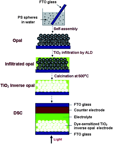 | ||
| Scheme 1 Schematics of the fabrication procedure of TIO electrodes under this study. | ||
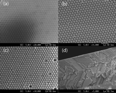 | ||
| Fig. 1 FESEM top-view images of initial opals formed from (a) 288 nm, (b) 390 nm, (c) 510 nm polystyrene spheres, and (d) cross-sectional view of 288 nm photonic crystal. | ||
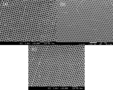 | ||
| Fig. 2 FESEM images of TiO2 inverse opals based on different size polystyrene opals. (a) 288 nm, (b) 390 nm and (c) 510 nm. | ||
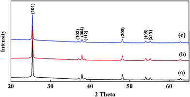 | ||
| Fig. 3 Powder XRD patterns of TiO2 inverse opals based on different size polystyrene opals. (a) 288 nm, (b) 390 nm and (c) 510 nm. | ||
The obtained TIOs can transmit light at a specific wavelength depending on the photonic lattice size of the TIOs. However, the measurement was difficult because the intensity was poor due to the thick films. Fortunately, the major optical signature can be measured through the specular reflectance measurements and compared to the calculated one using a Bragg diffractive equation (eqn (1)).
| λmax = 2d111neff sinθ | (1) |
| d111 = (2/3)1/2D | (2) |
| neff = [(ns)2f + (np)2(1 − f)]1/2 | (3) |
The specular reflectance spectra of initial opals, infiltrated opals, inverse opals, and dye-sensitized inverse opals with electrolytes are shown in Fig. 4. It is worth noting that the spectra of opals with different photonic lattice sizes show a similar trend in wavelength shifting when they were transformed from opal to dye-sensitized inverse opal. The spectra of initial opals (Fig. 4(a)) have a narrow bandwidth and their measured Bragg reflectance peaks were in excellent agreement with the one calculated by the Bragg equation (eqn (1)). After infiltrating amorphous TiO2 into the opals, the reflectance peaks (Fig. 4(b)) shifted to a higher wavelength due to the increased average effective refractive index. However, the spectra still remained sharp and symmetrical. The filling fractions were calculated to be 82.6, 83.3 and 84.2% of the total void volume for 288, 390 and 510 nm opals, respectively. This corresponds to 96.0, 96.9 and 97.9% of the maximum possible infiltration by conformal filling of fcc opal crystal. Higher filling fractions can reduce the cracks because a structural shrinkage is minimized after the high temperature decomposition and evaporation of the polystyrene spheres. Upon removing the polystyrene spheres from the infiltrated opals, a decrease in the mean effective refractive index of the structures has resulted in blue shifting of the reflectance peaks back to a lower wavelength (Fig. 4(c)). After immersing TIOs in dye and electrolyte solution, the Bragg peaks (Fig. 4(d)) shifted to a higher wavelength, but lower than the one measured for the TiO2 infiltrated opals. Based on these Bragg peak positions, the average refractive index of the electrolyte in TIO was calculated to be around 1.62, which is close to the refractive index of the MPN solvent, indicating complete filling of electrolyte within the air voids of TIO.
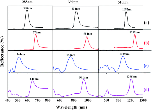 | ||
| Fig. 4 Specular reflectance spectra at 15° incidence measured for (a) initial opals, (b) infiltrated opals, (c) TiO2 inverse opals and (d) electrolyte-dye-sensitized TiO2 inverse opals formed from 288, 390 and 510 nm polystyrene spheres. | ||
Optoelectrical properties of TIOs in DSCs
Table 1 shows the open circuit photovoltage (VOC), short circuit photocurrent density (JSC), fill factor (FF), and power conversion efficiencies of DSCs with TIO electrodes of different photonic lattice sizes. A notable result is that the photocurrent decreases with increasing TIO sizes, leading to a decrease of power conversion efficiency. The TIO electrode of a size 288 nm shows the highest photocurrent density of 4.97 mA cm−2, and a power conversion efficiency of 2.22%. This size-dependent results are in contrast to the one reported by Kwak et al.18 They showed that the power conversion efficiency decreases with size reduction, even though the surface area of the structure increases with size reduction. They attributed this anomaly to the poor interfacial contact between the TIO and the conducting substrate due to partial infiltration of TiO2 nanoparticles in opal, which has resulted in an inverse relationship of solar cell efficiency to the surface area of TIO. In our results, the highly precise nature of the infiltration method by the ALD enables the fabrication of the high quality TIO structure for all photonic sizes as proven by the optoelectrical measurements. Hence, the ALD is a superior technique to achieve high infiltration and obtain high quality TIO electrodes for DSC applications.| Size/nm | V OC/V | J SC/mA cm−2 | FF | η (%) |
|---|---|---|---|---|
| 288 | 0.692 | 4.97 | 0.627 | 2.22 |
| 390 | 0.679 | 3.84 | 0.671 | 1.81 |
| 510 | 0.681 | 2.96 | 0.687 | 1.42 |
Comparing to the conventional TiO2 nanoparticle electrode with the same dye,33 the photocurrent of a TIO electrode is much lower than that of the conventional one due to the fact that the TIO has a smaller surface area and thus less dye loading. This in turn leads to the poor light absorption and light harvesting. However, considering the surface area of TIO electrodes is ∼ 14–25 times smaller than that of the nanoparticle electrode (assuming the nanoparticles are ∼20 nm in size diameter and the electrode film has the same thickness as the TIO electrode), the photocurrent generated per dye molecule on TIO electrodes is actually much superior to that on the nanoparticle electrode (without a scattering layer) since their photocurrent difference is no more than 4 times the best DSC using the same dye reported so far,33 suggesting efficient light trapping/scattering within TIO electrodes.
The IPCE of a DSC can be defined as34
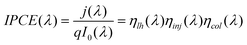
Fig. 5(a) shows the IPCE spectra of DSCs with different TIO electrode sizes. The result is consistent with the one observed from the I–V characteristics, showing that the TIO288 electrode has the highest quantum efficiency in most of the measured wavelength range. Unlike the wavelength dependency observed in the photocurrent as a function of TIO electrode sizes, the IPCE is different among the three TIO electrodes. Although the TIO288 electrode presents the highest IPCE at shorter wavelength, its quantum yield becomes lower than that of TIO390 at longer wavelength (Fig. 5(a)). This trend becomes more apparent when their IPCE spectra were normalized using their peak maxima (Fig. 5(b)). All three TIO electrodes show an almost identical quantum yield at wavelength shorter than 580 nm but longer than 450 nm, indicating that they share the same phenomenon of charge injection and collection within the wavelength range. However, at wavelength longer than 580 nm, TIO390 demonstrates the highest quantum efficiency while TIO288 is the lowest one. This difference can be understood by correlating the quantum efficiency with the respective reflectance spectra. When the incident photon wavelength is shorter than 580 nm, there is almost no feature of selective reflection for all three electrodes (Fig. 4(d)). The light harvesting is purely determined by the surface area of the electrode, being consistent with the identical quantum efficiency of the normalized spectra. On the contrary, when the incident photon wavelength is longer than 580 nm but shorter than 700 nm, TIO288 presents very strong reflection between 600 and 700 nm, while TIO510 only has modest reflection, and TIO390 has no appreciable reflection. As a consequence, TIO390 benefits from the large amount of photon absorption, whereas TIO288 suffers the largest loss of incident photons as they were reflected by the electrode.
 | ||
| Fig. 5 (a) Incident photon to current conversion efficiency (IPCE), (b) IPCE curves normalized to the maximum value, and (c) relative enhancement factor versus wavelength for inverse-opal TiO2/FTO dye sensitized solar cells. | ||
The absorption of D149 dye as well as most of the other commonly used dyes decreases significantly at longer wavelengths (> 700 nm).35,36 At wavelength of 700 nm, the extinction coefficient of the D149 molecule is very low. A slight attenuation of the incident light at this wavelength region will strongly affect the light harvesting. As a result, TIO288 and TIO510 give almost no response in the IPCE measurement and this may be attributed to the strong reflectance of the two TIO electrodes to the photons with wavelength of more than 700 nm. In comparison, TIO390 has almost no reflection at ∼700 nm. Consequently, some light harvesting was observed for TIO390, while none for TIO288 and TIO510 (Fig. 5(b)). This difference is further illustrated in Fig. 5(c) where it shows the relative increment of TIO390 and TIO510 with respect to TIO288. The largest difference of IPCE appears at λ = 640 nm, corresponding to the maximum reflectance of TIO288 and minimum reflectance of TIO390 (Fig. 4(d)).
The selective reflection of TIO electrodes and its influence on the IPCE spectrum are important considerations if TIOs were to be used as dielectric mirrors to enhance light harvesting of DSCs. As shown in Fig. 4(d), TIO electrodes of different sizes show different reflectance maxima. To enhance the absorption, the reflectance spectrum of the TIO electrode should be tuned to complement the absorption spectrum of the light absorber. For example, the absorption spectrum of D149 dye has a maximum at ∼530 nm but tails off gradually from 530 to 700 nm. To enhance the harvesting of these long wavelength photons (from 530 to 700 nm), a TIO layer with a reflectance maximum at this wavelength range is highly desired as it can reflect the light back to the electrode for further light absorption. Therefore, the result showed that TIO288 would be a desired material as a dielectric mirror to combine with a mesoporous TiO2 layer since it has the strongest reflectance to the photons between 600 and 700 nm.
4. Conclusions
In conclusion, it is the first attempt of TIOs being fabricated by the ALD method and being used as photoanodes for DSC applications. ALD is the preferred technique to achieve high infiltration and to obtain high quality TIO electrodes because it can achieve more than 96% of the maximum possible infiltration. The power conversion efficiencies of 2.22, 1.81 and 1.42% were achieved with TIO of sizes 288, 390 and 510 nm, respectively. When compared to the conventional nanocrystalline TiO2 type of photoanode in DSC, TIO electrode showed weaker absorption due to its low surface area for dye loading. However, the selective reflection of single-layer TIO electrodes and their influence on the IPCE spectra that were revealed in this study provide new insights into their potential application as a dielectric mirror on the photoanode or on the counter electrode. The high quality TIOs can act as a dielectric mirror by coupling it on a nanocrystalline TiO2 layer that reflects the incident photons back to the dye, and at the same time it can act as a photoanode to effectively harness the transmitted light for enhancing the light harvesting of DSCs.Acknowledgements
This work was supported by the Ministry of Education, Singapore by Tier 2 Academic Research Fund under grant number T208A1225, ARC 5/08.References
- E. Yablonovitch, Phys. Rev. Lett., 1987, 58, 2059 CrossRef CAS.
- S. John, Phys. Rev. Lett., 1987, 58, 2486 CrossRef CAS.
- S. John and T. Quang, Phys. Rev. Lett., 1997, 78, 1888 CrossRef CAS.
- J. S. Foresi, P. R. Villeneuve, J. Ferrera, E. R. Thoen, G. Steinmeyer, S. Fan, J. D. Joannopoulos, L. C. Kimerling, H. I. Smith and E. P. Ippen, Nature, 1997, 390, 143 CrossRef CAS.
- K. Busch and S. John, Phys. Rev. E, 1998, 58, 3896 Search PubMed.
- R. Biswas, M. M. Sigalas, G. Subramania and K.–M. Ho, Phys. Rev. B, 1998, 57, 3701 CrossRef CAS.
- R. Biswas, M. M. Sigalas, G. Subramania, C. M. Soukoulis and K.–M. Ho, Phys. Rev. B, 2000, 61, 4549 CrossRef CAS.
- T. Honda, K. Yanashima, J. Yoshino, H. Kukimoto, F. Koyama and K. Iga, Jpn. J. Appl. Phys., 1994, 33, 3960 CrossRef CAS.
- S. Chao, W.–H. Wang and C.–C. Lee, Appl. Optics, 2001, 40, 2177 CrossRef CAS.
- T. Yokogawa, S. Yoshii, A. Tsujimura, Y. Sasai and J. Merz, Jpn. J. Appl. Phys., 1995, 34, L751 CrossRef CAS.
- V. Pore, A. Rahtu, M. Leskelä, M. Ritala, T. Sajavaara and J. Keinonen, Chem. Vap. Deposition, 2004, 10, 143 CrossRef CAS.
- S. Ichikawa and R. Doi, Thin Solid Films, 1997, 292, 130 CrossRef CAS.
- S. Nishimura, N. Abrams, B. A. Lewis, L. I. Halaoui, T. E. Mallouk, K. D. Benkstein, J. van de Lagemaat and A. J. Frank, J. Am. Chem. Soc., 2003, 125, 6306 CrossRef CAS.
- I. Rodriguez, P. Atienzar, F. Ramiro-Manzano, F. Meseguer, A. Corma and H. Garcia, Photonics and Nanostructures-Fundamentals and Applications, 2005, 3, 148 Search PubMed.
- L. I. Halaoui, N. M. Abrams and T. E. Mallouk, J. Phys. Chem. B, 2005, 109, 6334 CrossRef CAS.
- C. L. Huisman, J. Schoonman and A. Goossens, Solar Energy Materials & Solar Cells, 2005, 85, 115 Search PubMed.
- S. -H. A. Lee, N. M. Abrams, P. G. Hoerz, G. D. Barber, L. I. Halaoui and T. E. Mallouk, J. Phys. Chem. B, 2008, 112, 14415 CrossRef CAS.
- E. S. Kwak, W. Lee, N.–G. Park, J. Kim and H. Lee, Adv. Funct. Mater., 2009, 19, 1093 CrossRef CAS.
- S. Guldin, S. Hüttner, M. Kolle, M. E. Welland, P. Müller-Buschbaum, R. H. Friend, U. Steiner and N. Tétreault, Nano Lett., DOI:10.1021/nI904017t.
- A. Mihi and H. Míguez, J. Phys. Chem. B, 2005, 109, 15968 CrossRef CAS.
- A. Mihi, F. J. López-Alcaraz and H. Míguez, Appl. Phys. Lett., 2006, 88, 193110 CrossRef.
- A. Mihi, M. E. Calvo, J. A. Anta and H. Míguez, J. Phys. Chem. C, 2008, 112, 13 CrossRef CAS.
- J. S. King, D. Heineman, E. Graugnard and C. J. Summers, Applied Surface Science, 2005, 244, 511 CrossRef CAS.
- T. Suntola, Thin Solid films, 1992, 216, 84 CrossRef CAS.
- V. Pore, A. Rahtu, M. Leskelä, M. Ritala, T. Sajavaara and J. Keinonen, Chem. Vap. Deposition, 2004, 10, 143 CrossRef CAS.
- M. Leskelä and M. Ritala, Thin Solid Films, 2002, 409, 138 CrossRef CAS.
- O. Sneh, R. B. Clark-Phelps, A. R. Londergan, J. Winkler and T. E. Seidel, Thin Solid Films, 2002, 402, 248 CrossRef CAS.
- S. K. Karuturi, L. Liu, L. T. Su, Y. Zhao, H. J. Fan, X. Ge, S. He and A. I. Y. Tok, J. Phys. Chem. C, 2010, 114, 14843 CAS.
- S. O. Kucheyev, J. Biener, T. F. Baumann, Y. M. Wang, A. V. Hamza, Z. Li, D. K. Lee and R. G. Gordon, Langmuir, 2008, 24, 943 CrossRef CAS.
- G. M. Sundaram, E. W. Deguns, R. Bhatia, M. J. Dalberth, M. J. Sowa and J. S. Becker, Solid State Technology, 2009, 52, 12 CAS.
- J. S. King, E. Graugnard and C. J. Summers, Adv. Mater., 2005, 17, 1010 CrossRef CAS.
- L. M. Fortes, M. C. Gonçalves and R. M. Almeida, J. Non-Crystalline Solids, 2009, 355, 1189 CrossRef CAS.
- S. Ito, S. M. Zakeeruddin, R. Humphry-Baker, P. Liska, R. Charvet, P. Comte, M. K. Nazeeruddin, P. Péchy, M. Takata, H. Miura, S. Uchida and M. Grätzel, Adv. Mater., 2006, 18, 1202 CrossRef CAS.
- J. R. Jennings and Q. Wang, J. Phys. Chem. C, 2010, 114, 1715 CrossRef CAS.
- K. MdZazeeruddin, R. Humphry-Baker, P. Liska and M. Grätzel, J. Phys. Chem. B, 2003, 107, 8981 CrossRef CAS.
- H. J. Snaith, A. Petrozza, S. Ito, H. Miura and M. Grätzel, Adv. Funct. Mater., 2009, 19, 1810 CrossRef CAS.
| This journal is © The Royal Society of Chemistry 2011 |