Exploring the fundamental effects of deposition time on the microstructure of graphene nanoflakes by Raman scattering and X-ray diffraction
Navneet
Soin
a,
Susanta Sinha
Roy
*a,
Christopher
O'Kane
a,
James A. D.
McLaughlin
a,
Teck H.
Lim
b and
Crispin J. D.
Hetherington
b
aNanotechnology and Integrated Bio-Engineering Centre, School of Engineering, University of Ulster, Newtownabbey, BT37 0QB, UK. E-mail: s.sinha-roy@ulster.ac.uk
bDepartment of Materials, University of Oxford, Parks Road, Oxford, OX1 3PH, UK
First published on 8th September 2010
Abstract
A systematic study is reported of the growth of vertically aligned few layered graphene (FLG) nanoflakes on Si (100) substrates by microwave plasma enhanced chemical vapour deposition (MPECVD) method. Asymmetric grazing incident angle X-ray diffraction (GIAXRD) studies revealed a structural transformation, from nanocrystalline graphite layers to FLG, with the increase of growth time. As the growth time increased we observed a preferred vertical orientation of FLGs accompanied by a sharp decrease in the d002 spacing. Transmission electron microscopy shows these structures have highly graphitized edge planes which terminate in a few layers (1–3) of graphene sheets. Detailed Raman studies not only support the structural transformation but also confirm that the process occurs via the sudden release of stress in nanocrystalline turbostratic graphite films. Graphical plot of all major Raman parameters (such as G peak position, ID/IG value, FWHM of D, G, and G′ peaks) vs.growth time shows a well defined trend. Using the graphical plots a tentative trajectory of the Raman parameters is proposed, which can be very useful in understanding structural transformation during growth process. Finally, a possible growth mechanism of FLGs is presented.
1. Introduction
Graphene, a single sheet of sp2 hybridised carbon atoms essentially forms the basis of all carbon nanostructures.1 The formation of carbon nanostructures stems from the presence of topological defects in sp2graphene sheets and eventually the graphene sheets fold onto themselves to form structures ranging from fullerenes to carbon nanotubes.1,2 Recently, 2D structures such as monolayered and few layered graphene sheets have been synthesized via routes such as mechanical exfoliation,1,2 epitaxial growth,3 vigorous chemical exfoliation of graphite,4 ultra high vacuum annealing of SiC surfaces,5chemical vapour deposition (CVD) on lattice matched substrates6 and microwave plasma enhanced chemical vapour deposition (MPECVD).7,8 Some of the methods such as mechanical exfoliation from HOPG surfaces, UHV annealing and epitaxial growth are very elaborate in nature and cannot be scaled up for mass production. However, methods such as chemical reduction of graphite oxide to graphene and chemical vapour deposition (CVD) including microwave plasma enhanced CVD (MPECVD) show more promise as they can be scaled up easily while providing high reproducibility.4In the literature, there is no consensus in naming few layered graphene (FLG) flakes, other than FLG they are often described as carbon nanowalls, nanoflakes, carbon nanosheetsetc.9–11 In general, FLGs is entirely different from other materials like carbon nanowalls which are more commensurate with highly defective nanostructured graphite.12 The FLG flake like structures grown without the use of any catalyst are predominantly made up of vertically stacked two dimensional graphene sheets, growing from the underlying substrate which terminates into open graphitic edge planes and sheets on top. While this catalyst free growth seems attractive especially for applications such as bioelectronics sensing and for electrochemical studies, the growth mechanism of these FLGs is not entirely understood; especially with regards to the initial nucleation stages and how the subsequent vertical alignment comes about. Earlier reports by Malesevic et al.7 have hypothesized that the release of stress is responsible for the vertical orientation of the flakes and indicated that the growth of FLGs follows a three step process.
Here, we report the results of systematic study of time dependence growth of few layered graphene (FLG) nanoflakes. The transmission electron microscopy confirms the growth of FLG nanoflakes. We, for the first time provide direct evidence using in depth Raman and X-ray analysis that the vertical orientation of FLGs is brought about via stress release at growing graphitic edges, responsible for orientation change from an in plane growth to vertical growth. Also, we suggest that the growth of FLGs proceeds via the nucleation of highly stressed nanocrystalline graphite layers.
2. Materials and methods
The synthesis of FLGs was carried out in SEKI Microwave Plasma Enhanced Chemical Vapour (MPECVD) deposition system, equipped with a 1.5 kW, 2.45 GHz microwave source. The substrates used were bare n type Si wafers (10 mm × 10 mm), cleaned viaultrasonication in acetone/DI water. The cleaned Si wafer was then placed on top of a thicker Si substrate and chamber pumped down via a rotary pump to ∼ 2 × 10⁻³ Torr. Once the desired base pressure was obtained, N2 plasma at 700 W was excited for certain duration of time during which the substrate temperature increased to ∼1200 °C, as monitored by an optical pyrometer on top of the chamber. CH4 was injected at the end of pre treatment time and growth carried out for different durations of time. The samples were allowed to cool down up till room temperature under a N2 atmosphere. In literature H2 has been used instead of N2 during the growth of FLGs.7,10 The use of nitrogen instead of hydrogen is advantageous as hydrogen plasma preferably etches amorphous as well as graphitic phases synthesised and may attack the nucleation sites during the growth process. For simplicity, the deposition conditions mentioned above is shown schematically in Fig. 1.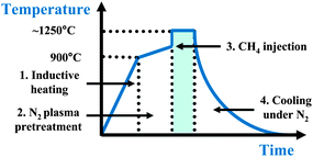 | ||
| Fig. 1 Illustration of FLG growth process with different stages (1–4). 1. Heating of the sample from room temperature to 900 °C via inductive heating under N2 flow. 2. N2 plasma pre-treatment for approx. 10 min. 3. CH4 injection at the end of pre-treatment for FLG growth. 4. Cooling to ambient under N2 flow. | ||
Scanning electron microscopy was performed on a FEI Quanta 300D operating at 30 kV. TEM analysis was performed on a JEOL JEM-4000EX HREM operating at 100 kV, for which samples were scraped off the surface and deposited on a 300 mesh holey carbon grids. AFM studies were carried out using a Veeco Nanoman DI 300 system. In order to study the growth process of FLG system, Raman spectroscopy was performed using an ISA LabRam system equipped with a 632.8 nm He–Ne laser with a spot size of ∼ 2–3 μm, yielding a spectral resolution of better than 2 cm−1. Due care was given to minimise sample heating by using a lower laser power below 2 mW. Grazing incident angle X-ray diffraction (GIAXRD) studies were carried out on a Bruker D8 advance XRD system with a Cu Kα radiation (0.154 nm) with a 0.06 degree step size and an acquisition time of 15 s/step. Scans were also performed in triplicate at 0.02 degree step size and an acquisition time of 60 s per step to accurately determine the C(002) peak as well as corresponding d002 spacing.
3. Results and discussion
3.1 Growth of FLGs
The overall morphology and structure of the FLGs were characterized by scanning electron microscopy (SEM), atomic force microscopy (AFM) and transmission electron microscopy (TEM). Fig. 2 shows the SEM images of the FLGs at various growth times from 15 s to 10 min. The films consist of flake like structures with randomly interwoven sharp edges with open spaces between them. As evident from the SEM images of Fig. 2, with the increase in the growth time, the degree of interlinking increased along with an overall increase in the height of the flakes. It is worthwhile to point out here that during the initial growth stage, there is some degree of interlinking however many sheets could have folded under their own weight, thus displaying orientations spread out from 0° to 90° with respect to the substrate (Fig. 2a). At higher growth times, the enhanced interlinking possibly makes the structures stiffer and thereby making them stand perpendicular to the surface more (Inset Fig. 2d).13Fig. 3 shows a cross-sectional area of Focussed Ion Beam (FIB) milled sample in which the aggregation of individual flakes can be observed. The aggregates are direct evidence that the growth proceeds via the amalgamation of separate nucleation centres, instead of formation of a continuous thin film. The TEM analysis (Fig. 4) confirmed that the flakes were indeed made up of large number of edges with the presence of graphene layers and graphitic steps. Low magnification image shows a crumpled sheet like morphology and with sheets possibly stacked over one another, it produces a variation in thickness under the electron beam and hence the contrast can be observed. The flakes show predominantly a knife like structure with a thicker base ∼ 15–20 nm which constantly narrows down along the axial growth direction, until at the top where there are only 1–3 graphene layers present. The calculated (002) plane spacing of 0.342–0.339 nm from XRD, also confirmed by TEM is more commensurate with single crystal graphite (0.335 nm) in comparison to previously reported carbon nanosheets (0.37 nm) by Wang et al.14 Also, no amorphous carbon deposition was detected on the outside of FLG unlike those found during the growth of carbon nanowalls on SiO2.15 Thus, the FLGs deposited by this method show a higher crystallinity than carbon nanowalls and nanosheets reported earlier. | ||
| Fig. 2 Scanning electron microscopy (SEM) images of FLGs at various growth times, (A) 15 s, (B) 60 s, (C) 180 s, and (D) 600 s. Inset shows the vertical alignment of the FLGs to the underlying Si substrate. | ||
 | ||
| Fig. 3 FIB milled cross sectional image of FLG sample. The presence of voids is indicative that the growth proceeds via amalgamation of different nucleation sites. | ||
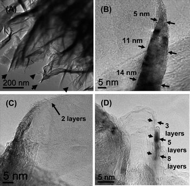 | ||
| Fig. 4 Transmission electron microscopy (TEM) images of FLGs at (a) low magnification showing extensive edges. High resolution images showing, (b) knife edge like structure narrowing at the top, (c) continuous reduction of graphene layers to reveal only bilayered graphene at the top, (d) trilayered graphene at flake edge. | ||
3.2 X-ray diffraction study
The preferred orientation of various aligned carbon nanostructured systems such as aligned CNTs has been studied by techniques such as Near Edge X-ray Absorption Fine spectroscopy (NEXAFS), however they require intense tunable source of soft X- rays which are available at synchrotron stations only.16–18 In our case we have made use of asymmetric grazing incident angle X-ray diffraction (GIAXRD) to assess the preferred orientation of FLG system and provided evidence of their growth mechanism. Similar XRD geometry has been used in the past by other groups to assess vertical alignment of carbon nanowalls.13,19,20Fig. 5 shows the asymmetric XRD scans for varying growth times from 15 s to 10 min. Fig. 6 shows the variation of the diffraction angle and FWHM of the (002) peak as a function of growth time. The peaks in the XRD scans correspond to the hexagonal graphite structure. With the increase in the growth time, the increase in the intensity and reduction of the Full Width at Half Maxima (FWHM) of C (002) peak can be observed. Also, the carbon peak at approx. 2θ = 42.7°, corresponding to a combination of turbostratic graphite and crystalline graphite appears to be building up at longer growth times.13,19 Turbostratic carbon is essentially a two dimensional structure in which even though the interlayer distance (0.342 nm) approaches that of crystalline graphite (0.335 nm), they possess no periodicity as the layers are misaligned to each other either by translation or rotation.19,21 The (00l) reflections are observed due to the consistent layer spacing, but for truly crystalline material such as HOPG, only full (hkl) indices reflections can be observed.19,21 While there are conflicting reports by French13,19 and Yoshimura20 on the presence of turbostratic carbon in FLG and FLG like systems, the peak position and peak shapes observed are indicative of the presence of turbostratic carbon. Previous reports by French et al.13,19 have confirmed the presence of turbostratic graphite in carbon nanosheets. As the growth time increases the reduction in the FWHM of the C (002) peak, along with the increase in the relative intensity can be observed, indicative of higher crystallinity, accompanied by an upshift of the C (002) 2θ peak (Fig. 6). Calculation of the graphene interlayer spacing revealed that there is a significant reduction in the d002 spacing as the growth time is increased, from 0.342 nm for 20 s growth time to around 0.339 nm for 10 min growth (Fig. 5 inset). The increase in the stacking along the z axis, along with a reduction in the d002 spacing can be attributed to the increased number of graphene layers being added to the flakes, which increase the long-range, inter atomic attractive forces causing the sheets to collapse together and thereby decreasing the d002 value. These results are consistent with results previously observed by French et al.13 Recent computer simulation results show that the curvature of the graphene layers have significant impact on the FWHM and diffraction angle of C (002) peak. The decreases of FWHM and increases of C (002) peak position with increasing growth time (Fig. 6) can also be related to the decrease of curvature of graphene layers, as in this case overall curvature decreases due to the increased number of graphene layers with deposition time.
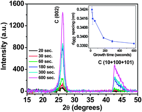 | ||
| Fig. 5 Asymmetric grazing angle XRD scans of FLGs grown for various times. Inset shows the change in the d002 spacing with increase in growth time. | ||
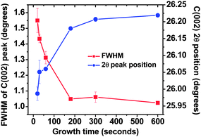 | ||
| Fig. 6 Variation of FWHM and peak position of C (002) peak with the increase of growth time. | ||
Also, in Fig. 5 the change in the peak shape of C ((10) + (100) + (101)) peak can be observed and becomes increasingly symmetric at higher growth times. At lower growth times (at 15–20 s) the peak at 2θ = 42.7° cannot be observed, however there is a gradual build-up of the peak after 30 s of growth time. It is not possible for a sample with adequate layers stacked together to yield (00l) reflection and not also yield (hk) reflection, the absence of this peak at small growth times can thus be attributed to a change in the average orientation of the layers in the sample.13,19
3.3 Raman spectroscopy
The Raman spectra of nearly all carbon based material exhibit at least three to four major bands, denoted as D, G, D′ and G′(2D) band.22–24 The defect induced band, D, does not have any dependence on the number of graphene layers but only depends solely on the amount of disorder present.16–18,22–24 The G peak corresponds to the stretching vibration mode, E2g phonon at the Brillouin zone centre. The D′ peak originates from the symmetry breaking due to finite sp2 crystallite size and appears as a shoulder of the G band.25 In recent report,26 the origin of Raman D and D′ bands is clearly understood by double resonance theory. The D band is associated with an inter-valley double resonance process, whereas the D′ band comes from an intra-valley double resonance process.26 The 2D peak is the second order of the D peak which originates via a participation of two phonons with opposite wave vectors (q and −q) leading to momentum conservation. The appearance of D peak requires defects whereas the 2D band does not require defects for its activation. Thus, the appearance of 2D peak is treated as a fingerprint of crystalline carbon materials.25–27 The transition from bulk graphite to nanocrystalline graphite and vice-versa produces pronounced effects in the Raman spectra, especially with the intensity ratio of the D and G peak, ID/IG. The smaller crystalline grains as well as the interdefect distance produces higher ID/IG ratio, along with an increased FWHM (Γ) of the bands.22–25Fig. 7 shows the normalized Raman spectra of FLG samples at various growth times and provides important insights into the nucleation and growth of FLGs. It can be clearly observed that the nucleation of FLGs starts in between 10 and 15 s after the injection of CH4 into the chamber, suggesting that there is a 10–12 s lag time in the nucleation of in-plane basal graphene sheets and onset of subsequent vertical alignment which is the growth phase. This lag time is far less than those reported for Radio Frequency Plasma Enhanced Chemical Vapor Deposition (RF PECVD) system used by other research groups.10 The primary reason for this is that the effective electron and flux densities in microwave plasma are at least two orders higher than an inductively/capacitively coupled RF plasma source. Resemblance (shape of the peaks and position) of the Raman spectra of samples grown between 15 and 20 s (Fig. 7) were very similar to the nanocrystalline graphite.28 As growth time increased, D peak intensity decreased and G peak intensity increased progressively. Also, the peak position of the D band moves from 1328 cm−1 for 20 s growth time to 1336 cm−1 for growth time of 10 min, whereas the G′ band moved from 2658 cm−1 to 2665 cm−1 for above mentioned growth time (Fig. 7). These phenomena may be linked to the overall increase in the number of edge planes which are continuously being added by the increase in the number of graphene layers causing an enhanced interlinking between flakes. The D band is accompanied by a shoulder near 1620 cm−1, whose intensity decreases with the increase in growth time. The appearance of this band has been associated with the presence of the crystalline edge and has also been related to the lattice defects present in the crystal.29–31
 | ||
| Fig. 7 Normalized Raman spectra for FLGs at various growth times, showing the transition from nanocrystalline graphite to FLGs. The black spectrum shows no growth was observed until 10 s after the addition of CH4 into the chamber. The up shift of D and G′ bands is highlighted with the dotted line. | ||
We have attempted to elucidate the growth mechanism by analysing the Raman parameters of films across a range of growth times from 10 s to 10 min. To obtain the peak positions and widths correctly, fit of the first order spectral bands was performed with Lorentzian function for D and G band and a Gaussian function for the D′ band. This provides a natural convergence and does not induce any shifts in the G band.32 The fit of second order spectra (G′) was performed using Lorentzian functions. Apart from structural characterisation, in the past Raman spectra has been used for residual stress measurements in thin diamond like carbon (DLC) films.33 More recently, it has been applied to stress measurement in graphene.34 Usually, an increase in the stress is accompanied by the movement of G band to higher wave number. Fig. 8 shows the plot of G peak position and ID/IG ratio as a function of growth time. The G peak position sharply decreased by ∼ 5 cm−1 as the growth time increased from 15 s to 30–60 s. The blue shift of G band has been previously attributed to an increase in the strong compressive strain of graphene layers.34 Also, G peak movement has recently been attributed to the change in the number of layers by Gupta et al.35 Thus, a red shift in the observed G band position in our study could be a combination of reduction in the compressive stress and an increase in the number of layers. After 60 s of growth time, there is a slight increase of G peak position which is possibly due to the formation of graphitic nanoflakes at higher growth times. The ID/IG ratio in our samples showed a similar trend to the G peak positions with the change in the deposition time (Fig. 8). In carbon based nanomaterials, ID/IG value changes due to the following two factors. Firstly, defects in crystalline structure and secondly, due to the edge defects (such as edge shape and curvature). At the onset of nucleation at 15 s growth time, ID/IG ratio is very high (∼ 2.1) with a large G FWHM (Γ) of 40 cm−1 indicating that these nucleation sites are predominantly made up of highly defective/distorted nanocrystalline graphite in the form of graphene sheets. However, increase in the growth time from 15 s to 30 s immediately improves the overall crystallinity, as seen by the drastic change in the ID/IG (0.93) ratio. As the growth time increased beyond 60 s, ID/IG ratio started to increase again due to an increased number of edges present on the surface as well as their more inclination towards vertical direction, which contribute heavily towards the Raman scattering. Above 5 min of growth time we did not observe any increase in the value of ID/IG. The high value of ID/IG ratio, as compared to recent works by other groups observed is caused by a large number of edges normal to the surface and the high density of these flakes on the surface.7,36,37 For carbon based materials the excitation energy has a strong correlation with peak positions and peak intensities and a part of the high ID/IG ratio may be attributed to the longer excitation wavelength used in this study. Also, the values of IG/IG′ followed a similar trend to the ID/IG values, with a minimum value of ∼ 0.9 at 30 s growth time.
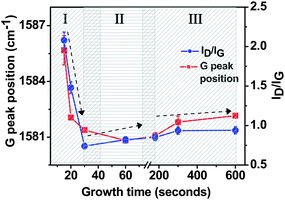 | ||
| Fig. 8 Plot of G peak position vs.growth time showing the stress release and corresponding change in the ID/IG ratio showing the change in the overall microstructure of FLGs. Error bars denote standard deviation. Region I represents nanocrystalline graphite region, region II represents FLG system and region III represents graphitic nanoflakes. Arrows mark the possible trajectory of the graph. | ||
The FWHM values (Γ) of all the bands, depicted in Fig. 9 follow a similar trend where they rapidly reduce during the initial nucleation and growth of the structure and then increase with the increase in growth time. For graphitic films, a low ID/IG ratio and a narrow FWHM of the G band are indicative of a higher quality film.38 We observed a dramatic reduction in the G band FWHM to ∼ 22.5 cm−1 from 40 cm−1 (Fig. 9) for the films grown at 30 s. One of the indicators of FLG like systems is the narrow FWHM of the G′ band near 2650 cm−1 along with the absence of a shoulder.7,39 In our studies the G′ FWHM reduced from about 60 cm−1 at 15 s to about 40 cm−1 for 30 s and this value does not changed significantly up to 60 s growth. As reported by other groups, the value of FWHM for few layered graphene like systems lies within the range of 35 to 50 cm−1.6,40 The FWHM of G′ band is also reported to be ∼25 cm−1 for monolayer graphene.26 Similar nature and shape of the G′ band was found by Malesevic et al. in their growth of few layered graphene system on silicon and other metals.7 It is also in agreement with previous results by various authors who have observed for CVD derived few graphene layers on SiC and metals, one, two and three layered graphene samples, all exhibit a single and sharp Lorentzian G′ band.6,7,39,41–44 For higher growth times above 5 min, the FWHM increased due to increased number of edges present on the surface as well as the edge thickness which contribute towards the Raman scattering. The ID/IG value has been used extensively to evaluate the in plane sp2 crystallite size, La, in disordered carbon materials. In this report, we have determined La from the following general formula described by Cançado et al. for nanographitic material, for any excitation energy (EL) of laser source:28
 | (1) |
 | ||
| Fig. 9 Variation of FWHM of Raman bands (■) D band; (●) G band; (▲) G′ band at different growth times and its inverse dependence to the crystallite size (◊).Region I represents nanocrystalline graphite region, region II represents FLG system and region III represents graphitic nanoflakes. | ||
Fig. 9 also shows the plot of Lavs.growth time. The full width at half maximum (Γ) of all peaks was roughly proportional to 1/La, showing the phonon life time (τ) was proportional to crystalline size.
Taking into account the plots of (i) FWHM of all peaks, (ii) G peak position, (iii) ID/IG ratio and (iv) Lavs.growth time and their quantitative values, the following observations can be made: (i) the first stage of growth (nucleation) process exhibit a high density of defects inside the stressed nanocrystalline graphite. (ii) After 20–30 s of growth a stress release mechanism leads to phase transformation from highly stressed nanocrystalline graphite to few layered graphene. This is clearly indicated by the sharp change of all the Raman parameters. (iii) The optimum time range for growth of FLG systems is between 30 s and 60 s, (iv) beyond 60–90 s, Raman parameters did not show any significant change possibly due to the addition of multiple graphene layers. Based on the above observations a simple trajectory (shown by arrows) of all Raman parameters with respect to growth time is shown in Fig. 8 and 9. This trajectory can be divided into three different regimes. Region I is described as a nano-crystalline graphitic region, where a high density of defects exists. The structures existing within this regime are highly stressed with a turbostratic graphite like structure as evident by an upshift of the G band to higher wavenumbers. This, along with an enhanced d002 spacing of 0.342 nm as well as the high Raman FWHM of the G′ band provides a compelling evidence of the existence of highly stressed turbostratic nanographite in region I. Region II can be ascribed as the growth window for few layered graphene (FLG) like system. It is characterised by a dramatic reduction in the Raman FWHM of the G′ band as well as a red shift of the G band. The evidence for FLG like system is also provided by the TEM images shown in Fig. 4. Finally, region III is attributed as the initial stage of graphitic nanoflakes. In this regime, there is an addition of large number of graphene sheets causing an increase in the edge thickness. The addition of these multiple layers leads to an increase in the long-range interatomic attractive forces causing the sheets to collapse together. This manifests into an up shift of 2θ position and a calculated d002 spacing of 0.339 nm approaching that of graphite (0.335 nm).
In general, high resolution TEM (and corresponding selected area electron diffraction) and X-ray diffraction studies are employed to evaluate stacking order in graphitic materials. Recently, Raman studies on heat-treated disordered graphite films, showed that the G′ peak shape, width and positions can be used to infer information about the degrees of stacking order.45 For the FLG samples we observed a clear variation in the G′ line shape (Fig. 7 and Fig. 9). At the initial stage G′ peak is wider, the peak becomes sharper and more intense as the growth time increase and finally wider again as the growth time was further increased (Fig. 9). At the initial stage single Lorentzian with larger linewidth is the signature of 2D graphite, hence no stacking order between adjacent graphene layers.45 At the second stage sharp G′ line, indicates that an ordered stacking (i.e., ABAB stacking) has formed in some regions of the FLGs. Although G′ width increases significantly at higher growth time, we have not observed two-peaks in G′ line, which is the typical profile for the 3D graphite samples. This suggests electronic coupling between graphene layers may not occur in all regions of the FLGs and there is a certain degree of ABAB stacking disorder.6 This interpretation is consistent with our transmission electron microscopy studies, where we found local stacking order of graphene layers was not the same all over the samples but a continuous reduction of graphene layers on the top knife edges (Fig. 4).
In Fig. 10 we have highlighted the possible growth mechanism using schematic and AFM measurements. The growth proceeds via the nucleation of highly stressed and defective nanocrystalline graphite which do not have any stacking order, except for lattice spacing matching close to that of turbostratic graphite present as graphene sheets which starts to grow parallel to the substrate. As the number of graphene sheets being added start to increase, there is an increase in the size of the flake in all directions (Fig. 10a) This increase in the flake size accompanied by other internal stress inducing factors such as temperature gradient and ion bombardment, causes higher stress at grain boundaries of individual flakes. The interaction between the edges of these growing nanoflakes promotes a release of stress thereby causing a change in the overall alignment of these nanoflakes from being parallel to the substrate to that of being vertically aligned (Fig. 10b).7,10,46Fig. 10c and Fig. 10d show the AFM image of FLGs at growth times of 20 and 60 s. It was observed that FLGs present a robust net-like structure with a high degree of interlacing which increases with growth time. At 60 s (Fig. 10d) of growth an optimal wall like structure can be clearly observed while at longer growth times an increase in the individual wall thickness can be observed (not shown here). Also, in plasma based growth systems, the effect of electric field in promoting vertical alignment cannot be ruled out. Bower et al. have shown previously that aligned carbon nanotubes can be grown perpendicular to the local substrate surface, regardless of the surface tilt.47 This alignment is induced by the electrical self-bias field imposed on the substrate surface from the plasma environment. In the growth of FLGs, once the geometry of the sheets has turned from in-plane to out of plane via stress release as shown in Fig. 10b, the high surface mobility of incoming carbon-bearing species and the induced polarization of graphitic layers causes the FLGs to grow perpendicular to the substrate.10 In a high carbon bearing flux environment any carbon-bearing species which diffuse towards the in plane growth region of substrate instead of the growing edges (acting as nucleation centres) will get re-evaporated because of weak Van der Waals interaction between the substrate and the carbon-bearing species.10 Thus, at an optimal growth time, this accounts for the wall like morphology observed in the AFM image of Fig. 10d which essentially terminates into 1–3 layers of graphene at the top.
 | ||
| Fig. 10 Schematic showing the (a) growth and interaction of nanoflakes, (b) stress release via change in the orientation during the first 15–20 s of growth (black hexagons denote in plane graphene layer, whereas red hexagons denote out of plane vertical graphene layer). AFM images of structural evolution of FLG nanoflakes at (c) 20 s., (d) 60 s. The interconnection of flakes and increased edge formation can be clearly observed. | ||
4. Conclusion
Few layered graphene (FLG) nanoflakes were deposited on Si substrate with preferred vertical orientation and possessing a large number of highly graphitised knife like edges. The XRD analysis show an increased crystallinity evident by reduction in FWHM and an upshift in the C (002) position. By analyzing the changes in the Raman parameters with the structural information obtained by X-ray diffraction and microscopic studies, we show that the growth of these FLGs proceeds via the nucleation of highly stressed nanocrystalline turbostratic graphite and the vertical orientation is brought by the release of stress at longer growth times. Dispersion of Raman parameters with deposition time provide direct experimental evidence of phase transformation from turbostratic graphite to FLG. Three clear regions in the trajectory of all Raman parameters proved to be effective in classifying three different phases; nanocrystalline graphite, FLGs and graphitic nanoflakes. These FLG systems could have potential applications in electrochemical based biosensors, field emission sources and catalysis.Acknowledgements
The EPSRC is thanked for funding the access to the TEM instruments in Oxford Materials under the Materials Equipment Access scheme, grant reference: EP/F01919X/1. We are grateful to Dr Gareth Hughes at Dept. of Materials at University of Oxford for his help with FIB milling and Dr Patrick Lemoine at NIBEC for his help with AFM studies.References
- K. S. Novoselov, A. K. Geim, S. V. Morozov, D. Jiang, Y. Zhang, S. V. Dubonos, I. V. Grigorieva and A. A. Firsov, Science, 2004, 306, 666 CrossRef CAS.
- K. S. Novoselov, D. Jiang, F. Schedin, T. J. Booth, V. V. Khotkevich, S. V. Morozov and A. K. Geim, Proc. Natl. Acad. Sci. U. S. A., 2005, 102, 10451 CrossRef CAS.
- P. W. Sutter, J.-I. Flege and E. A. Sutter, Nat. Mater., 2008, 7, 406 CrossRef CAS.
- S. Gilje, S. Han, M. Wang, K. L. Wang and R. B. Kaner, Nano Lett., 2007, 7, 3394 CrossRef CAS.
- K. V. Emtsev, F. Speck, T. Seyller, J. D. Riley and L. Ley, Phys. Rev. B: Condens. Matter Mater. Phys., 2008, 77, 155303 CrossRef.
- A. Reina, X. Jia, J. Ho, D. Nezich, H. Son, V. Bulovic, M. S. Dresselhaus and J. Kong, Nano Lett., 2009, 9, 30 CrossRef CAS.
- A. Malesevic, R. Vitchev, K. Schouteden, A. Volodin, L. Zhang, G. V. Tendeloo, A. Vanhulsel and C. V. Haesendonck, Nanotechnology, 2008, 19, 305604 CrossRef.
- G. D. Yuan, W. J. Zhang, Y. Yang, Y. B. Tang, Y. Q. Li, J. X. Wang, X. M. Meng, Z. B. He, C. M. L. Wu, I. Bello, C. S. Lee and S. T. Lee, Chem. Phys. Lett., 2009, 467, 361 CrossRef.
- N. G. Shang, F. C. K. Au, X. M. Meng, C. S. Lee, I. Bello and S. T. Lee, Chem. Phys. Lett., 2002, 358, 187 CrossRef CAS.
- M. Zhu, J. J. Wang, B. C. Holloway, R. A. Outlaw, X. Zhao, K. Hou, V. Schutthanandan and D. M. Manos, Carbon, 2007, 45, 2229 CrossRef CAS.
- Y. Wu, P. Qiao, T. Chong and Z. Shen, Adv. Mater., 2002, 14, 64 CrossRef CAS.
- A. T. H. Chuang, J. Robertson, B. O. Boskovic and K. K. K. Koziol, Appl. Phys. Lett., 2007, 90, 123107 CrossRef.
- B. L. French, J. J. Wang, M. Y. Zhu and B. C. Holloway, J. Appl. Phys., 2005, 97, 114317 CrossRef.
- J. J. Wang, M. Y. Zhu, O. X. Zhao, D. M. Manos, B. C. Holloway and V. P. Mammana, Appl. Phys. Lett., 2004, 85, 1265 CrossRef CAS.
- K. Tanaka, M. Yoshimura, A. Okamoto and K. Ueda, Jpn. J. Appl. Phys., 2005, 44, 2074 CrossRef CAS.
- S. Banerjee, T. Hemraj-Benny, S. Sambasivan, D. A. Fischer, J. A. Misewich and S. S. Wong, J. Phys. Chem. B, 2005, 109, 8489 CrossRef CAS.
- G. Abbas, P. Papakonstantinou, G. R. S. Iyer, I. W. Kirkman and C. L. Chen, Phys. Rev. B: Condens. Matter Mater. Phys., 2007, 75, 195429 CrossRef.
- N. G. Shang, P. Papakonstantinou, M. McMullan, M. Chu, A. Stamboulis, A. Potenza, S. S. Dhesi and H. Marchetto, Adv. Funct. Mater., 2008, 18, 3506 CrossRef CAS.
- B. L. French, J. J. Wang, M. Y. Zhu and B. C. Holloway, Thin Solid Films, 2006, 494, 105 CrossRef CAS.
- H. Yoshimura, S. Yamada, A. Yoshimura, I. Hirosawa, K. Kojima and M. Tachibana, Chem. Phys. Lett., 2009, 482, 125 CrossRef CAS.
- Z. Q. Li, C. J. Lu, Z. P. Xia, Y. Zhou and Z. Lou, Carbon, 2007, 45, 1686 CrossRef CAS.
- A. C. Ferrari and J. Robertson, Phys. Rev. B: Condens. Matter Mater. Phys., 2000, 61, 14095 CrossRef CAS.
- F. Tuinstra and J. L. Koenig, J. Chem. Phys., 1970, 53, 1126 CrossRef CAS.
- A. C. Ferrari and J. Robertson, Phys. Rev. B: Condens. Matter Mater. Phys., 2001, 64, 075414 CrossRef.
- J. Kastner, T. Pichler, H. Kuzmany, S. Curran, W. Blau, D. N. Weldon, M. Delamesiere, S. Draper and H. Zandbergen, Chem. Phys. Lett., 1994, 221, 53 CrossRef CAS.
- L. M. Malard, M. A. Pimenta, G. Dresselhaus and M. S. Dresselhaus, Phys. Rep., 2009, 473, 51 CrossRef CAS.
- C. Casiraghi, A. Hartschuh, H. Qian, S. Piscanec, C. Georgi, A. Fasoli, K. S. Novoselov, D. M. Basko and A. C. Ferrari, Nano Lett., 2009, 9, 1433 CrossRef CAS.
- L. G. Cancado, K. Takai, T. Enoki, M. Endo, Y. A. Kim, H. Mizusaki, A. Jorio, L. N. Coelho, R. Magalhães-Paniago and M. A. Pimenta, Appl. Phys. Lett., 2006, 88, 163106 CrossRef.
- K. Yasushi and K. Gen, Phys. Rev. B: Condens. Matter, 1995, 52, 10053 CrossRef.
- R. Saito, A. Jorio, A. G. Souza Filho, G. Dresselhaus, M. S. Dresselhaus and M. A. Pimenta, Phys. Rev. Lett., 2001, 88, 027401 CrossRef.
- P. H. Tan, C. Y. Hu, J. Dong, W. Shen and B. Zhang, Phys. Rev. B: Condens. Matter Mater. Phys., 2001, 64, 214301 CrossRef.
- V. Mennella, G. Monaco, L. Colangeli and E. Bussoletti, Carbon, 1995, 33, 115 CrossRef.
- J.-K. Shin, C. S. Lee, K.-R. Lee and K. Y. Eun, Appl. Phys. Lett., 2001, 78, 631 CrossRef CAS.
- Z. H. Ni, H. M. Wang, Y. Ma, J. Kasim, Y. H. Wu and Z. X. Shen, ACS Nano, 2008, 2, 2301 CrossRef CAS.
- A. Gupta, G. Chen, P. Joshi, S. Tadigadapa and P. C. Eklund, Nano Lett., 2006, 6, 2667 CrossRef CAS.
- D. Graf, F. Molitor, K. Ensslin, C. Stampfer, A. Jungen, C. Hierold and L. Wirtz, Nano Lett., 2007, 7, 238 CrossRef.
- L. Zeng, H. Peng, W. Wang, Y. Chen, W. Qi, D. Lei, J. Liang, J. Zhao and X. Kong, J. Phys. Chem. C, 2008, 112, 10735 CrossRef CAS.
- A. Yoshida, Y. Kaburagi and Y. Hishiyama, Carbon, 2006, 44, 2333 CrossRef CAS.
- A. C. Ferrari, J. C. Meyer, V. Scardaci, C. Casiraghi, M. Lazzeri, F. Mauri, S. Piscanec, D. Jiang, K. S. Novoselov, S. Roth and A. K. Geim, Phys. Rev. Lett., 2006, 97, 187401 CrossRef CAS.
- Y.-H. Lee and J.-H. Lee, Appl. Phys. Lett., 2009, 95, 143102 CrossRef.
- M. A. Pimenta, G. Dresselhaus, M. S. Dresselhaus, L. G. Cancado, A. Jorio and R. Saito, Phys. Chem. Chem. Phys., 2007, 9, 1276 RSC.
- P. Poncharal, A. Ayari, T. Michel and J. L. Sauvajol, Phys. Rev. B: Condens. Matter Mater. Phys., 2008, 78, 113407 CrossRef.
- D. S. Lee, C. Riedl, B. Krauss, K. von Klitzing, U. Starke and J. H. Smet, Nano Lett., 2008, 8, 4320 CrossRef CAS.
- A. Ismach, C. Druzgalski, S. Penwell, A. Schwartzberg, M. Zheng, A. Javey, J. Bokor and Y. Zhang, Nano Lett., 2010, 10, 1542 CrossRef CAS.
- L. G. Cancado, K. Takai, T. Enoki, M. Endo, Y. A. Kim, H. Mizusaki, N. L. Speziali, A. Jorio and M. A. Pimenta, Carbon, 2008, 46, 272 CrossRef CAS.
- A. N. Obraztsov, E. A. Obraztsova, A. V. Tyurnina and A. A. Zolotukhin, Carbon, 2007, 45, 2017 CrossRef CAS.
- C. Bower, O. Zhou, W. Zhu, D. J. Werder and S. Jin, Appl. Phys. Lett., 2000, 77, 2767 CrossRef CAS.
| This journal is © The Royal Society of Chemistry 2011 |