DOI:
10.1039/C0CE00220H
(Paper)
CrystEngComm, 2011,
13, 158-166
Facile on-demand oriented growth of perovskite oxide thin films: applications of Dion–Jacobson phase as seed layer
Received
21st May 2010
, Accepted 8th July 2010
First published on 27th August 2010
Abstract
We investigated a new fabrication process for high-quality, uniaxial-oriented grown Dion–Jacobson perovskite (DJP) RbLaNb2O7 thin films by means of excimer laser assisted metal organic deposition. Oriented crystal growth occurred only by excimer laser irradiation in air at 400 °C after a deposition of metal–organic solution and preheating at 400 °C. The obtained RbLaNb2O7 thin film showed perfect (010)-oriented growth on borosilicate glass substrates, and the film surface had atomically flat terraces. We confirmed that the obtained DJP RbLaNb2O7 thin films functioned very well as a seed layer for the fabrication of various perovskite oxide thin films with high orientation quality. An oriented grown LaNiO3 thin film fabricated on the DJP seed layer and prepared at 400 °C exhibited low electrical resistivity at room temperature. Moreover, we demonstrated the utility of our methodology for on-demand fabrication by combining our method with an inkjet printing technique to pattern LaNiO3 thin films with a line shape, which also were successfully grown with uniaxial orientation on the DJP seed layer. A ferroelectric Na0.5K0.5NbO3 perovskite film was heteroepitaxially grown on the uniaxial-oriented grains of the LaNiO3/RbLaNb2O7 thin film, and this oriented film exhibited a higher dielectric constant than that of a film fabricated without the DJP seed layer. Thus, we demonstrated facile, oriented crystal growth enabled by the uniaxial-oriented DJP seed layer.
Introduction
Physical properties of oxide thin films are strongly dependent on their crystal quality. In particular, control of crystal orientation is considered to be one of the most important issues in obtaining good properties of oxide thin film materials, and to date such control has generally been achieved by designing surface structures on substrates to promote specific crystal orientations. For many studies of oxide thin films, single crystal oxide substrates such as SrTiO3, LaAlO3, α-Al2O3, and MgO have been used because of their precise surface structural control that enables high-quality crystal growth in particular orientations.1–5 However, the use of single crystal oxide substrates is not realistic for industrial applications due to the crystals' high cost and difficulty in up scaling. Therefore, crystal growth processes for high-quality oriented oxide thin films without single crystal substrates have been recently developed; some seed layer methods, such as ion beam assisted deposition and Langmuir–Blodgett nanosheet deposition.6–10 Though these processes have enabled the fabrication of high-quality, oriented oxide heterostructures, further improvements are still needed to allow on-demand fabrication of oriented films for oxide electronics applications, such as microelectromechanical systems (MEMS),11,12 owing to process restrictions associated with these applications. Thus, further development of oriented film growth techniques is an important issue for future high-integration applications.
In this study, we report a new process based on chemical solution deposition (CSD) for preparation of perovskite oxide multi-layered thin films with high-quality uniaxial orientation. The CSD process was very simple and enabled on-demand fabrication, in contrast to the conventional methods. To achieve the objectives, we employed an excimer laser-assisted metal organic deposition (ELAMOD) process developed from a conventional metal organic deposition (MOD) process.13–16 The ELAMOD process can be used to fabricate oxide thin films at low temperature for commonly used substrates such as Si and borosilicate glass, which cannot withstand high temperatures (T > 400 °C) in air: oxide films are crystallized by means of excimer laser irradiation (λ = 193, 248, and 308 nm) instead of by high-temperature furnace heating as is used in the MOD process. Details of the ELAMOD crystal growth mechanism are described elsewhere.15,16 In this study, we chose the Dion–Jacobson perovskite (DJP) oxide RbLaNb2O717–19 to prepare an oriented growth seed layer on amorphous glass substrates by means of the ELAMOD process. The crystal structure of RbLaNb2O7 (referred to herein as “DJP seed layer”) is shown in Fig. 1.19 The Rb ions and double-layered perovskite slabs are stacked alternately along the b-axis. We investigated the oriented growth of DJP seed layer thin films on amorphous glass substrates, and we demonstrate herein the fabrication of various multi-layered perovskite thin films on the obtained oriented RbLaNb2O7 seed layers.
 |
| | Fig. 1 Schematic crystal structure of RbLaNb2O7 used to fabricate DJP seed layer films. Rb ions and double-layered perovskite slabs are stacked alternately along the b-axis. | |
Experimental
Thin film fabrication procedures
DJP seed layer (RbLaNb2O7) thin films were fabricated by the ELAMOD process. The starting solutions for the RbLaNb2O7 films were prepared by mixing 2-ethylhexanoate solutions of the constituent metals diluted with toluene to obtain the required concentration and viscosity for spin-coating. The Rb![[thin space (1/6-em)]](https://www.rsc.org/images/entities/char_2009.gif) :La:Nb molar ratio in the coating solution was 1.0:1.0:2.0. This solution was spin-coated onto borosilicate glass substrates at 4000 rpm for 10 s. The coated films were preheated at 400 °C in air for 10 min to decompose the organic components of the films. The spin coating and preheating were repeated three times, and then the films were irradiated with a KrF laser (Lambda Physik Compex110) at an afluence of 60 mJ cm−2 and a pulse duration of 26 ns for 7500 pulses at 400 °C in air. The laser energy was homogenized by a beam homogenizer. Thereafter, the obtained RbLaNb2O7 thin films were used as a DJP seed layer for the preparation of various perovskite materials as described below. SrTiO3 thin films on borosilicate glass substrates with and without the DJP seed layer were prepared by means of the ELAMOD process. A mixed solution of strontium and titanium 2-ethylhexanoates (Sr:Ti = 1.0:1.0) diluted with toluene was spin-coated onto substrates at 4000 rpm for 10 s. The coated films were dried at 100 °C in air to remove the solvent, and then preheated at 400 °C in air for 10 min. The preheated films were irradiated with the KrF laser at an afluence of 75 mJ cm−2 for 7500 pulses at 400 °C in air. For conducting LaNiO3 thin films on borosilicate glass substrates with and without the DJP seed layer, lanthanum and nickel 2-ethylhexanoate solutions (La:Ni = 1.0:1.0) diluted with toluene were used as a starting solution. The solution was spin-coated onto substrates at 4000 rpm for 10 s. In addition, a line-shaped LaNiO3 thin film was also prepared on the DJP seed layer by deposition of the lanthanum–nickel starting solution using an inkjet printer (Microjet, FemtoJet). The deposited films were dried at 100 °C in air and then preheated at 400 °C in air for 10 min. The preheated films were irradiated with the KrF laser at an afluence of 50 mJ cm−2 for 5000 pulses at 400 °C in air. On the obtained bottom electrode LaNiO3 thin films, ferroelectric Na0.5K0.5NbO3 thin films were fabricated. The Na:K:Nb molar ratio in the coating solution was 1.0:1.0:2.0. This solution was spin-coated onto the LaNiO3 thin films at 4000 rpm for 10 s. The coated films were dried at 100 °C in air and preheated at 400 °C in air for 10 min. The preheated films were irradiated with the KrF laser at an afluence of 50 mJ cm−2 for 5000 pulses at 400 °C in air. The film thickness of each perovskite thin film on the seed layer was increased by repeating the coating, preheating, and laser irradiation processes. All of the processes were carried out at low temperature (<400 °C) in air.
:La:Nb molar ratio in the coating solution was 1.0:1.0:2.0. This solution was spin-coated onto borosilicate glass substrates at 4000 rpm for 10 s. The coated films were preheated at 400 °C in air for 10 min to decompose the organic components of the films. The spin coating and preheating were repeated three times, and then the films were irradiated with a KrF laser (Lambda Physik Compex110) at an afluence of 60 mJ cm−2 and a pulse duration of 26 ns for 7500 pulses at 400 °C in air. The laser energy was homogenized by a beam homogenizer. Thereafter, the obtained RbLaNb2O7 thin films were used as a DJP seed layer for the preparation of various perovskite materials as described below. SrTiO3 thin films on borosilicate glass substrates with and without the DJP seed layer were prepared by means of the ELAMOD process. A mixed solution of strontium and titanium 2-ethylhexanoates (Sr:Ti = 1.0:1.0) diluted with toluene was spin-coated onto substrates at 4000 rpm for 10 s. The coated films were dried at 100 °C in air to remove the solvent, and then preheated at 400 °C in air for 10 min. The preheated films were irradiated with the KrF laser at an afluence of 75 mJ cm−2 for 7500 pulses at 400 °C in air. For conducting LaNiO3 thin films on borosilicate glass substrates with and without the DJP seed layer, lanthanum and nickel 2-ethylhexanoate solutions (La:Ni = 1.0:1.0) diluted with toluene were used as a starting solution. The solution was spin-coated onto substrates at 4000 rpm for 10 s. In addition, a line-shaped LaNiO3 thin film was also prepared on the DJP seed layer by deposition of the lanthanum–nickel starting solution using an inkjet printer (Microjet, FemtoJet). The deposited films were dried at 100 °C in air and then preheated at 400 °C in air for 10 min. The preheated films were irradiated with the KrF laser at an afluence of 50 mJ cm−2 for 5000 pulses at 400 °C in air. On the obtained bottom electrode LaNiO3 thin films, ferroelectric Na0.5K0.5NbO3 thin films were fabricated. The Na:K:Nb molar ratio in the coating solution was 1.0:1.0:2.0. This solution was spin-coated onto the LaNiO3 thin films at 4000 rpm for 10 s. The coated films were dried at 100 °C in air and preheated at 400 °C in air for 10 min. The preheated films were irradiated with the KrF laser at an afluence of 50 mJ cm−2 for 5000 pulses at 400 °C in air. The film thickness of each perovskite thin film on the seed layer was increased by repeating the coating, preheating, and laser irradiation processes. All of the processes were carried out at low temperature (<400 °C) in air.
Sample characterization
The crystal structure and orientation properties of the obtained films were studied by X-ray diffraction measurements (Rigaku, SmartLab). 2θ − β maps (β: the direction along Debye rings), a χ − ϕ map, and micron-scale analysis were obtained with a two-dimensional (2D) pixel area detector (Dectris, PILATUS 100 K)20 and a collimator with 200 μm diameter. The detector length from the samples was fixed at 102 mm. The degree of crystal orientation was evaluated in terms of the Lotgering factor F, which is calculated from the following equation.21
| F(hkl) = (P − P0)/(1 − P0) |
where P0 = ΣI0(hkl)/ΣI0(HKL) and P = ΣI(hkl)/ΣI(HKL). I0 and I are the intensities of each of the diffraction peaks in X-ray diffraction patterns as presented in ICSD database and in experimental data, respectively. The relative growth rate of the crystal planes was determined for each facet area of the RbLaNb2O7 as calculated by the Bravais–Friedel Donnay–Harker (BFDH) method22 using a Materials Studio program package. The crystal growth process and crystallinity of the thin films were observed by cross-sectional transmission electron microscopy (XTEM) and selected area electron diffraction (SAED) analysis using a JEM-2010 (JEOL) instrument operating at 200 kV. The samples for the XTEM observations were prepared by argon milling using an ion milling device (BAL-TEC, RES100). The surface of the samples was studied with an atomic force microscope (AFM). The electrical resistivity curves of the LaNiO3 thin films as a function of temperature were measured by a four-probe technique. The dielectric constants of the Na0.5K0.5NbO3 thin films were collected at 1 kHz with a LCR meter (WAYNE KERR, 6440A).
Results and discussion
Oriented growth of Dion–Jacobson perovskite RbLaNb2O7 thin films
Fig. 2 shows the 2θ/ω scan of X-ray diffraction for a ELAMOD-fabricated DJP RbLaNb2O7 film with a thickness of 60 nm on a glass substrate. The RbLaNb2O7 film was very well crystallized without impurities, and all of the observed Bragg reflections were assigned to 0k0 indices without any other orientations. This assignment indicates that the film was grown with a strong (010) orientation, corresponding to the layered stacking direction of the DJP structure shown in the inset of Fig. 2. From the X-ray diffraction intensities, the Lotgering factor F(010) was estimated to be 1.0, indicating a perfect (010) orientation. To analyze the orientation quality of the obtained film, we evaluated 2D X-ray diffraction measurements. The 2θ − β map for the RbLaNb2O7 film is shown in Fig. 3a. The Bragg reflections corresponding to 0k0 indices appeared as spots at β = 0°. The β scan profiles for 020 and 080 reflections were collected from the obtained 2θ − β map. Both reflection profiles showed an obvious peak shape, and their full widths at half maximum (FWHM) were 3.70° and 3.85°, respectively. These values can be regarded as small for the crystal orientation quality on the amorphous glass substrates. Fig. 3c shows the χ − ϕ map around the 141 reflection. The 141 reflection was observed along χ = 55° at all values of ϕ. The obtained results indicate that the in-plane crystallized grains of the film had random orientations, although the in-plane crystal grain size appeared to be relatively large as evidenced by the inhomogeneous distribution of peak intensities. On the basis of these X-ray diffraction measurements, we confirmed that the fabricated RbLaNb2O7 film exhibited high-quality, uniaxial, (010)-oriented crystal growth.
 |
| | Fig. 2
X-Ray diffraction pattern for a DJP RbLaNb2O7 thin film on a borosilicate glass substrate (top), and the simulated pattern of polycrystalline RbLaNb2O7 with random orientation (bottom). The inset shows a schematic illustration for the relationship between the obtained film orientation and the substrate. | |
 |
| | Fig. 3 (a) 2θ − β map for a DJP RbLaNb2O7 thin film on a borosilicate glass substrate. (b) β scan profiles collected from the 2θ − β map at 2θ = 8.02° and 32.72° for 020 and 080 reflections, respectively. (c) χ − ϕ map around the 141 reflection. | |
Fig. 4 shows a high-resolution XTEM image (a) and the SAED pattern (b) of the prepared RbLaNb2O7 film along the [101] projection. The layered structure corresponding to the alternate stacking of Rb ions and double-layered perovskite slabs along the b-axis of RbLaNb2O7 was clearly observed in a direction normal to the substrate surface. The emerging stacking faults observed in the structure shown in Fig. 4a probably gave rise to the larger FWHM (ca. 3.70°) observed in β-scans of 0k0 X-ray diffraction peaks of the RbLaNb2O7 film compared to those of peaks generally observed in single crystals. Fig. 5a shows the XTEM image of the sample after the excimer laser irradiation at 3000 pulses to the amorphous precursor film. A crystalline, layered phase about 20 nm was confirmed at the film surface, and a partially crystalline phase was observed under the crystalline phase. The location of these phases indicates that the crystal growth of the RbLaNb2O7 thin film preferentially proceeded from the amorphous film surface to the interface with the glass substrate.
![(a) [101]-zone high-resolution XTEM image for a DJP RbLaNb2O7 thin film on a borosilicate glass substrate after excimer laser irradiation at 7500 pulses. The white arrows represent stacking faults of the DJP layered structure. (b) SAED pattern of the RbLaNb2O7 thin film.](/image/article/2011/CE/c0ce00220h/c0ce00220h-f4.gif) |
| | Fig. 4 (a) [101]-zone high-resolution XTEM image for a DJP RbLaNb2O7 thin film on a borosilicate glass substrate after excimer laser irradiation at 7500 pulses. The white arrows represent stacking faults of the DJP layered structure. (b) SAED pattern of the RbLaNb2O7 thin film. | |
![(a) [101]-zone high-resolution XTEM image for a DJP RbLaNb2O7 thin film after excimer laser irradiation at 3000 pulses, and brightness analysis of the obtained XTEM image as a function of depth. The brightness periodicity indicates the presence of a crystalline DJP phase, and one period of brightness intensity corresponds to one layer unit (1 l.u.) of the DJP structure as shown in the inset. (b) Schematic illustrations of the depth dependence of the temperature distribution under pulsed laser irradiation, and of the crystal growth process with increasing number of laser pulses.](/image/article/2011/CE/c0ce00220h/c0ce00220h-f5.gif) |
| | Fig. 5 (a) [101]-zone high-resolution XTEM image for a DJP RbLaNb2O7 thin film after excimer laser irradiation at 3000 pulses, and brightness analysis of the obtained XTEM image as a function of depth. The brightness periodicity indicates the presence of a crystalline DJP phase, and one period of brightness intensity corresponds to one layer unit (1 l.u.) of the DJP structure as shown in the inset. (b) Schematic illustrations of the depth dependence of the temperature distribution under pulsed laser irradiation, and of the crystal growth process with increasing number of laser pulses. | |
Two remarkable features associated with crystal growth of oxide films in the ELAMOD process should be noted here. First, when no effective crystal nucleation sites are present in an amorphous precursor film matrix, crystal nucleation occurs from the film surface, since the excimer laser irradiation induces a gradient temperature profile through a film thickness of several hundred nanometres due to a large photoabsorbance of the films (left panel of Fig. 5b).16 Second, epitaxial growth proceeds preferentially from active nucleation sites, provided that the sites have a large absorbance for the irradiated laser wavelength and a small lattice mismatch with the grown material.15 Therefore, the initial nucleation of crystalline RbLaNb2O7 on the glass substrate probably occurred at the amorphous precursor film surface under excimer laser irradiation. The film then would have grown epitaxially from those first nucleation sites at the film surface, as the crystallized RbLaNb2O7 has a large absorbance at the KrF excimer laser wavelength (248 nm). In addition, the potential feature of the crystal growth in RbLaNb2O7 is essential for the orientation growth in this process. Crystal facet area calculations associated with the crystal growth rates (Table 1) revealed that the {020} plane was largely preferred among the crystal facets of RbLaNb2O7, reflecting the two-dimensionality of the DJP layered structure. This suggests that the (010) orientation at the film surface would significantly reduce the surface energy in the crystal growth process. Hence, the growth mechanism of (010) orientation corresponding to the DJP layered structure in this process can be explained as follows. First, nucleation owing to the gradient temperature distribution induced by the excimer laser irradiation occurred at the film surface, while the (010)-layered structural ordering reduced the crystal surface energy. Then, the film grew epitaxially from the first (010)-oriented crystal nuclei toward the interface with the borosilicate glass substrate. Thus, we concluded that the uniaxial-oriented growth observed in this study was enabled by the complementary nature of the ELAMOD process to the DJP RbLaNb2O7 crystal growth.
Table 1 Relative stability of crystal facets for the DJP RbLaNb2O7
| {hkl} |
d(hkl)/Å |
Total facet area (%) |
| 020 |
10.995 |
54.03 |
| 011 |
5.329 |
19.38 |
| 101 |
3.884 |
26.58 |
| 200 |
2.747 |
0.01 |
The surface of the prepared RbLaNb2O7 film was observed by AFM (Fig. 6a), and the root-mean-squared surface roughness of the film was evaluated to be 9.46 nm. This value is large compared to that of commercial single crystal substrates. We conducted additional evaluations of the surface roughness of the film. Fig. 6b shows the XTEM image of the film around the variable thickness region that caused the surface roughness observed in the AFM image. It should be noted that the film surface in the flat region of the film (labelled 1 in Fig. 6b and 6c) was confirmed to be atomically flat, comparable to the surfaces of perovskite nanosheets and cleaved layered crystals.9,23–26 This flatness would have originated from the reduced crystal surface energy associated with the crystal growth of RbLaNb2O7 discussed above. Moreover, remarkable features were also observed in regions of varied thickness in the film (labelled 2 and 3 in Fig. 6b and 6c), including steps the size of layer units (the thickness of one layer unit is about 1.1 nm) and atomically flat terraces without ambiguous disordered lattice morphology. These results mean that the RbLaNb2O7 film had a clean (010) crystal surface, which is favorable for seed layers used to grow uniaxial-oriented perovskite heterostructures, at almost surface area, even though the film had a relatively large surface roughness. Thus, these results demonstrated perfect (010)-oriented growth of the DJP RbLaNb2O7 thin film at low temperature by means of the CSD-based ELAMOD process that we developed. In particular, we note that this process was extremely facile, involving only three steps: coating, preheating, and laser irradiation.
 |
| | Fig. 6 (a) AFM image of the surface of a DJP RbLaNb2O7 thin film. (b) XTEM image of the thin film after excimer laser irradiation at 7500 pulses, and (c) high-resolution XTEM images of the enlarged views for the regions labelled 1, 2, and 3 in (b). The black arrows indicate atomically flat surface regions. The red indicators represent one layer unit of the DJP structure. | |
Seed layer property of RbLaNb2O7 thin films for uniaxial-oriented growth of perovskites
We studied the utility of the obtained (010)-oriented DJP RbLaNb2O7 thin film as a seed layer for preparation of uniaxial-oriented perovskite oxide thin films. We prepared thin films of SrTiO3, which is a representative cubic perovskite oxide with lattice parameter a = 3.905 Å (the lattice mismatch of SrTiO3 with the b-plane of RbLaNb2O7 in the simple perovskite units is 0.53%),27 on glass substrates with and without the DJP seed layer by means of the ELAMOD process at 400 °C in air. The 2θ/ω scans of X-ray diffraction of the prepared SrTiO3 thin films with 60 nm thickness are shown in Fig. 7. On the bare glass substrate, the observed diffraction peaks were indexed to 100, 110, and 200 for the cubic SrTiO3, indicating almost random orientations: the Lotgering factor F(100) was evaluated to be 0.268. In contrast, the SrTiO3 film on the seed layer was well crystallized and showed a highly (100)-oriented growth. The main diffraction peaks were assigned to h00, whereas a trace of 110 peak intensity was also confirmed near 32.5° by multi-peak fittings. The Lotgering factor F(100) was calculated to be 0.983, which was significantly large.
 |
| | Fig. 7
X-Ray diffraction patterns for prepared films of RbLaNb2O7/glass (blue), SrTiO3/RbLaNb2O7/glass (red), and (c) SrTiO3/glass (black). The inset shows an enlarged view of each diffraction pattern at 31.5–34.0°. The subscripts R and S represent RbLaNb2O7 and SrTiO3, respectively. | |
Fig. 8a and 8b show the 2θ − β mappings for the obtained SrTiO3 films without and with the seed layer, respectively. Although the Bragg reflections of the SrTiO3 film without the seed layer exhibited spread Debye rings along β, those for the SrTiO3 film with the seed layer were clearly observed as defined spots. The β-scans for the 080 diffraction of the seed layer and 200 diffraction of the SrTiO3 film are shown in Fig. 8c. The FWHM of these peaks were 3.72° and 5.52°, respectively. These values suggest that the SrTiO3 film was well crystallized and oriented in the (100) direction with a nearly equivalent orientation quality in the seed layer. The slight deterioration of the FWHM value indicates that the increasing orientation distribution might have been caused by the imperfect surface flatness of the seed layer.
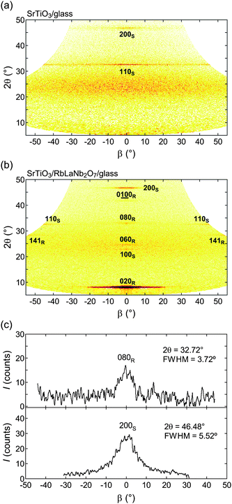 |
| | Fig. 8 2θ − β map for (a) SrTiO3/glass and (b) SrTiO3/RbLaNb2O7/glass. (c) β-scan profiles collected from the 2θ − β map for 080R (2θ = 32.72°) and 200S (2θ = 46.48°) reflections in SrTiO3/RbLaNb2O7/glass. The subscripts R and S represent RbLaNb2O7 and SrTiO3, respectively. | |
Fig. 9 shows the XTEM and SAED analyses for the prepared (100)-oriented SrTiO3 film grown on the DJP seed layer. The high-resolution lattice images and SAED patterns of both phases showed that the SrTiO3 film was grown epitaxially on the (010)-oriented grain of the seed layer: the cube-on-cube relationship was clearly maintained at the interface between the flat surface of the seed layer and the SrTiO3 film, suggesting that the (010)-oriented RbLaNb2O7 functioned well as the seed layer for the fabrication of perovskite oxide, uniaxial-oriented heterostructures.
 |
| | Fig. 9 (a) High resolution XTEM image of a prepared multi-layered SrTiO3/RbLaNb2O7 thin film on a borosilicate glass substrate. The enlarged lattice images and SAED patterns for (b) the SrTiO3 film and (c) the RbLaNb2O7 film are also shown. The subscript P represents the unit cell for the simple cubic perovskite. | |
Application of the DJP seed layer for conducting and ferroelectric perovskite materials
The pseudo-cubic perovskite LaNiO3 with a = 3.840 Å28 (the lattice mismatch is 1.15% with RbLaNb2O7 in the simple perovskite units) is well known as a material for conducting electrodes.29–33 Polycrystalline LaNiO3 thin films have exhibited electrical resistivity characteristic of a metallic material, about 0.5–2.0 mΩ cm, at room temperature.30–33 However, a relatively high process temperature (about 700–800 °C) was used to produce these metallic films. Therefore, we prepared metallic LaNiO3 films by means of the ELAMOD process with the DJP RbLaNb2O7 seed layer at a low process temperature (below 400 °C).
Fig. 10 shows the 2θ/ω scans of X-ray diffraction for the LaNiO3 films prepared at 400 °C in air with a thickness of ca. 100 nm with and without the DJP seed layer. The crystallized LaNiO3 film on the bare glass substrate showed random orientation growth without (100) orientation. In contrast, the LaNiO3 film on the seed layer was well crystallized and exhibited a significant enhancement of h00 diffraction peaks, which indicated the (100) orientation. The Lotgering factor F(100) of this film was calculated to be 0.971. The electrical resistivities (ρ) of the prepared LaNiO3 films with and without the DJP seed layer at room temperature as a function of film thickness are shown in Fig. 11. The ρ values for both samples decreased with increasing film thickness up to about 60 nm. At a film thickness of about 100 nm, ρ of the obtained LaNiO3 films with and without the DJP seed layer were 4.42 and 1.02 mΩ cm, respectively. Hence, the film with the DJP seed layer exhibited a 77% decrease in resistivity compared to the film on the bare substrate, and the temperature dependence of ρ was good metal to low temperature. Furthermore, the ρ value of the LaNiO3 film on the DJP seed layer was comparably lowered to that of the films prepared at high process temperatures in the previous reports.29–33
 |
| | Fig. 10
X-Ray diffraction patterns for prepared films of LaNiO3/RbLaNb2O7/glass (red) and LaNiO3/glass (black). The inset shows the enlarged view of each diffraction pattern at 31.5–34.0°. The subscripts R and L represent RbLaNb2O7 and LaNiO3, respectively. | |
 |
| | Fig. 11
ρ for LaNiO3/RbLaNb2O7/glass and LaNiO3/glass as a function of LaNiO3 film thickness. The inset shows the temperature dependence of ρ for LaNiO3/RbLaNb2O7/glass with a LaNiO3 thickness of ca. 100 nm. | |
Fig. 12a displays an optical microscope image of the line-shape patterned LaNiO3 film on the DJP seed layer after ELAMOD processing. The starting solution was deposited by an inkjet printer (see Experimental). The width and thickness of the patterned LaNiO3 wire film were evaluated to be 60 μm and 30 nm, respectively (inset of Fig. 12). Fig. 12b shows the 2θ-ω scan of the region including the patterned LaNiO3 film by using a ϕ200 μm X-ray collimator. All of the observed Bragg reflections were assigned to h00 peaks for LaNiO3 and 0k0 peaks for the DJP seed layer, indicating the successful (100)-oriented growth of the microscopic patterned LaNiO3 film. The compatibility of the ELAMOD process with the inkjet printing technique and with the DJP seed layer indicates that our developed method could be used for on-demand fabrication of uniaxial oriented perovskite oxide thin films, which would be very useful for integrated devices such as MEMS.
 |
| | Fig. 12 (a) Optical microscope image for a patterned LaNiO3 film on the DJP seed layer after excimer laser irradiation. The inset shows an AFM image for the patterned LaNiO3 film. (b) Microscopic analysis of X-ray diffraction for the patterned LaNiO3 film on the DJP seed layer. The inset shows the β-scan profile for the 200L (2θ = 47.46°) reflection. The subscripts R and L represent RbLaNb2O7 and LaNiO3, respectively. | |
We also observed the heteroepitaxial multi-layered structure of perovskite films on uniaxial oriented grains of the DJP seed layer. Ferroelectric Na0.5K0.5NbO3 thin films with a thickness of ca. 420 nm were fabricated on the aforementioned LaNiO3 thin films as a bottom electrode with and without the DJP seed layer by means of the ELAMOD process. Fig. 13 shows the 2θ/ω scans of X-ray diffraction for the Na0.5K0.5NbO3 thin films on the LaNiO3 electrode films with and without the seed layer. On the LaNiO3 thin film with random orientations, the Na0.5K0.5NbO3 thin film exhibited a weak (100) orientation; the Lotgering factor F(100) was calculated to be 0.552. In contrast, the Na0.5K0.5NbO3 thin film fabricated on the highly (100)-oriented LaNiO3 thin film was crystallized with uniaxial orientation: the Lotgering factor F(100) in this case was calculated to be 0.943. This result indicates the utility of the DJP seed layers for fabricating multi-layered, uniaxial-oriented growth of perovskite heterostructures. The small decrease in the uniaxial orientation of the Na0.5K0.5NbO3 thin film compared to that of the (100)-oriented LaNiO3 thin film might have been caused by the relatively large lattice mismatch (about 2.79%) between the films' respective perovskite unit cells.34
 |
| | Fig. 13
X-Ray diffraction patterns for prepared films of Na0.5K0.5NbO3/LaNiO3/RbLaNb2O7/glass (red) and Na0.5K0.5NbO3/LaNiO3/glass (black). The inset shows the temperature dependence of the relative dielectric constants for Na0.5K0.5NbO3 films with (red) and without (black) the DJP seed layer. The subscripts R, L, and N represent RbLaNb2O7, LaNiO3, and Na0.5K0.5NbO3, respectively. | |
The relative dielectric constants (εr) of the prepared samples at room temperature were measured by applying AC 0.1 V at 1 kHz frequency. The εr values for the Na0.5K0.5NbO3 thin films on the (100)-oriented and non-oriented LaNiO3 electrodes were 570 and 325, respectively. As shown in the inset of Fig. 13, enhancement of εr in the highly crystallized and oriented grown film was clearly observed over a wide temperature range including the two structural phase transition temperatures of Na0.5K0.5NbO3 near 218 °C (orthorhombic–tetragonal) and 420 °C (tetragonal–cubic)35–37 owing to the high crystal orientation degree and the grain growth effect as observed in the previous reports.38–40 The broader temperature dependence of εr in the obtained Na0.5K0.5NbO3 films compared to that of the ceramic samples could be caused by multiple phenomena, such as the strain effect from the substrate lattices, the thermal excitation of dipolar (double ionized oxygen vacancies and niobium ions) under the alternative electric field,41 and the smaller crystal grain size of the films compared to that of the ceramic samples.
Therefore, we demonstrated that the DJP seed layer prepared by the ELAMOD process was successfully utilized for the fabrication of uniaxial-oriented, multi-layered perovskite heterostructures. All of the fabrication process temperatures for the various perovskite oxide thin films were low, below 400 °C, and we also demonstrated that this process was suitable in combination with an inkjet printing technique for the on-demand fabrication of uniaxial-oriented grown perovskite oxide thin films.
Conclusions
A new fabrication process for high-quality, uniaxial-oriented grown DJP RbLaNb2O7 thin films by means of an ELAMOD process has been investigated: oriented crystal growth occurred only by excimer laser irradiation in air at 400 °C after deposition of a metal–organic solution and preheating at 400 °C. The obtained RbLaNb2O7 thin film exhibited perfect (010)-oriented growth on borosilicate glass substrates, and the film surface had atomically flat terraces. We confirmed that the characteristics of the obtained DJP thin films functioned very well as a seed layer for the fabrication of various perovskite oxide thin films with high orientation quality. An oriented grown LaNiO3 thin film prepared on the DJP seed layer at 400 °C exhibited a low electrical resistivity of 1.02 mΩ cm at room temperature. Moreover, we demonstrated the utility of our methodology for on-demand fabrication: a patterned LaNiO3 thin film deposited as a line shape by inkjet printing was successfully grown with uniaxial orientation on the DJP seed layer. A ferroelectric Na0.5K0.5NbO3 perovskite film was also heteroepitaxially grown on the uniaxial-oriented grains of the LaNiO3/RbLaNb2O7 thin film, and the oriented film showed a higher dielectric constant than that of a film grown without the seed layer. Thus, we demonstrated facile, oriented crystal growth enabled by the uniaxial-oriented DJP seed layer.
Acknowledgements
We are grateful to M. Ichihara at the Institute for Solid State Physics, the University of Tokyo, for his help as well as valuable discussions. The XTEM observations and electrical resistivity measurements were carried out at the facilities of the Materials Design and Characterization Laboratory, Institute for Solid State Physics, University of Tokyo.
References
- A. Brinkman, M. Huijben, M. Vanzalk, J. Huijben, U. Zeitler, J. C. Maan, W. G. van der Wiel, G. Rijnders, D. H. A. Blank and H. Hilgenkamp, Nat. Mater., 2007, 6, 493 CrossRef CAS.
- I. Vrejoiu, M. Alexe, D. Hesse and U. Gösele, Adv. Funct. Mater., 2008, 18, 3892 CrossRef CAS.
- S. J. May, P. J. Ryan, J. L. Robertson, J.-W. Kim, T. S. Santos, E. Karapetrova, J. L. Zarestky, X. Zhai, S. G. E. te Velthuis, J. N. Eckstein, S. D. Bader and A. Bhattacharya, Nat. Mater., 2009, 8, 892 CrossRef CAS.
- Y. Wakabayashi, D. Bizen, H. Nakao, Y. Murakami, M. Nakamura, Y. Ogimoto, K. Miyano and H. Sawa, Phys. Rev. Lett., 2006, 96, 017202 CrossRef CAS.
- S. A. Chambers, Adv. Mater., 2009, 21, 1622 CrossRef CAS.
- M. Q. Huang, J. Greek, S. Massing, O. Meyer, H. Reiner and G. Linker, Nucl. Instrum. Methods Phys. Res., Sect. B, 1999, 148, 793 CrossRef CAS.
- T. Kato, Y. Iijima, T. Muroga, T. Saitoh, T. Hirayama, I. Hirabayashi, Y. Yamada, T. Izumi, Y. Shiohara and Y. Ikuhara, Phys. C, 2003, 392–396, 790 CrossRef CAS.
- K. Kikuta, K. Noda, S. Okumura, S. Yamaguchi and S. Hirano, J. Sol-Gel Sci. Technol., 2007, 42, 381 CrossRef CAS.
- T. Shibata, K. Fukuda, Y. Ebina, T. Kogure and T. Sasaki, Adv. Mater., 2008, 20, 231 CrossRef CAS.
- T. Shibata, T. Ohnishi, I. Sakaguchi, M. Osada, K. Takada, T. Kogure and T. Sasaki, J. Phys. Chem. C, 2009, 113, 19096 CrossRef CAS.
- M. Heule, S. Vuillemin and L. J. Gauckler, Adv. Mater., 2003, 15, 1237 CrossRef CAS.
- S. W. Kirchoefer, E. J. Cukauskas, N. S. Barker, H. S. Newman and W. Chang, Appl. Phys. Lett., 2002, 80, 1255 CrossRef CAS.
- T. Tsuchiya, K. Daoudi, T. Manabe, I. Yamaguchi and T. Kumagai, Appl. Surf. Sci., 2007, 253, 6504 CrossRef CAS.
- T. Tsuchiya, I. Yamaguchi, T. Manabe, T. Kumagai and S. Mizuta, Mater. Sci. Semicond. Process., 2002, 5, 207 CrossRef CAS.
- T. Nakajima, T. Tsuchiya, M. Ichihara, H. Nagai and T. Kumagai, Chem. Mater., 2008, 20, 7344 CrossRef CAS.
- T. Nakajima, T. Tsuchiya, M. Ichihara, H. Nagai and T. Kumagai, Appl. Phys. Express, 2009, 2, 023001 Search PubMed.
- M. Dion, M. Ganne and M. Tournoux, Mater. Res. Bull., 1981, 16, 1429 CrossRef CAS.
- J. Gopalakrishnan, V. Bhat and B. Raveau, Mater. Res. Bull., 1987, 22, 413 CrossRef CAS.
- A. R. Armstrong and P. A. Anderson, Inorg. Chem., 1994, 33, 4366 CrossRef.
- P. Kraft, A. Bergamaschi, Ch. Broennimann, R. Dinapoli, E. F. Eikenberry, B. Henrich, I. Johnson, A. Mozzanica, C. M. Schlepütz, P. R. Willmott and B. Schmitt, J. Synchrotron Radiat., 2009, 16, 368 CrossRef CAS.
- F. K. Lotgering, J. Inorg. Nucl. Chem., 1959, 9, 113 CrossRef CAS.
- J. D. H. Donnay and D. Harker, Amer. Mineralogist, 1937, 22, 446 Search PubMed.
- M. M. Treacy, S. B. Rice, A. J. Jacobson and J. T. Lewandowski, Chem. Mater., 1990, 2, 279 CrossRef CAS.
- R. E. Schaak and T. E. Mallouk, Chem. Mater., 2000, 12, 3427 CrossRef CAS.
- Y. Wakabayashi, M. H. Upton, S. Grenier, J. P. Hill, C. S. Nelson, J.-W. Kim, P. J. Ryan, A. I. Goldman, H. Zheng and J. F. Mitchell, Nat. Mater., 2007, 6, 972 CrossRef CAS.
- R. Matzdorf, Ismail, T. Kimura, Y. Tokura and E. W. Plummer, Phys. Rev. B: Condens. Matter Mater. Phys., 2002, 65, 085404 CrossRef.
- R. J. Nelmes, G. M. Meyer and J. Hutton, Ferroelectrics, 1978, 21, 461 CAS.
- A. Wold, B. Post and E. Banks, J. Am. Chem. Soc., 1957, 79, 4911 CrossRef CAS.
- K. Sreedhar, J. Honig, M. Darwin, M. McElfresh, P. Shand, J. Xu, B. Crooker and J. Spalek, Phys. Rev. B: Condens. Matter, 1992, 46, 6382 CrossRef CAS.
- A.-D. Li, C.-Z. Ge, D. Wu, P. Lü, Y.-Q. Zuo, S.-Z. Yang and N.-B. Ming, Thin Solid Films, 1997, 298, 165 CrossRef CAS.
- K. Ueno, W. Sakamoto, T. Yogo and S. Hirano, Jpn. J. Appl. Phys., 2001, 40, 6049 CrossRef CAS.
- D. Bao, X. Yao, N. Wakiya, K. Shinozaki and N. Mizutani, J. Phys. D: Appl. Phys., 2003, 36, 1217 CrossRef CAS.
- L. Yang, G. Wang, C. Mao, Y. Zhang, R. Liang, C. Soyer, D. Rémiens and X. Dong, J. Cryst. Growth, 2009, 311, 4241 CrossRef CAS.
- T. Saito, T. Wada, H. Adachi and I. Kanno, Jpn. J. Appl. Phys., 2004, 43, 6627 CrossRef CAS.
- Y. P. Guo, K. Kakimoto and H. Ohsato, Appl. Phys. Lett., 2004, 85, 4121 CrossRef CAS.
- B. Zhang, L. Zhang, J. Li, X. Ding and H. Zhang, Ferroelectrics, 2007, 358, 188 CrossRef CAS.
- D. Lin, K. W. Kwok and H. L. W. Chan, Appl. Phys. Lett., 2007, 90, 232903 CrossRef.
- C.-R. Cho and A. Grishin, Appl. Phys. Lett., 1999, 75, 268 CrossRef CAS.
- H. Takao, Y. Saito, Y. Aoki and K. Horibuchi, J. Am. Ceram. Soc., 2006, 89, 1951 CrossRef CAS.
- K. Shibata, K. Suenaga, A. Nomoto and T. Mishima, Jpn. J. Appl. Phys., 2009, 48, 121408 CrossRef.
- J. Miao, X. G. Xu, Y. Jiang, L. X. Cao and B. R. Zhao, Appl. Phys. Lett., 2009, 95, 132905 CrossRef.
|
| This journal is © The Royal Society of Chemistry 2011 |
Click here to see how this site uses Cookies. View our privacy policy here.