Correlating the scattered intensities of P3HT and PCBM to the current densities of polymer solar cells†‡
Enrique D.
Gomez
*a,
Katherine P.
Barteau
a,
He
Wang
ab,
Michael F.
Toney
c and
Yueh-Lin
Loo
*a
aDepartment of Chemical and Biological Engineering, Princeton University, Princeton, NJ 08544, USA. E-mail: edg12@psu.edu; lloo@princeton.edu
bDepartment of Electrical Engineering, Princeton University, Princeton, NJ 08544, USA
cStanford Synchrotron Radiation Lightsource, Menlo Park, CA 94025, USA
First published on 30th September 2010
Abstract
Grazing-incidence X-ray diffraction and rocking scans have quantified the structure of poly(3-hexylthiophene) and [6,6]-phenyl-C61-butyric acid methyl ester in the active layers of organic solar cells. Our study reveals that the device JSC correlates with the local structural development of pure PCBM and, to second order, the extent of out-of-plane P3HT π-stacking.
It is well documented that the processing conditions of organic solar cells comprising poly(3-hexylthiophene), P3HT, can have strong influences on device performance.1–5 For example, thermal or solvent-vapor annealing of the active layer has led to increases in the short-circuit current densities (JSC) of P3HT/[6,6]-phenyl-C61-butyric acid methyl ester, or PCBM, solar cells; this improvement in device performance has been attributed to enhancements of the polymer crystallinity.6–9 Given that the active layer consists of a blend of a polymer and a small molecule, its phase separation and crystallization characteristics are necessarily complex and interdependent on the aggregation and crystallization of the constituents. Yet, the details of how such processing affect the structuring of PCBM remains unclear. We have examined, for the first time, the structure of the individual constituents in the active layers of bulk–heterojunction organic solar cells comprising P3HT and PCBM in relation to the device JSC by quantifying the X-ray scattered intensity acquired during both grazing-incidence X-ray diffraction and rocking scan (or local specular) experiments. We find the structure of PCBM is most important in determining device JSC; the extent of out-of-plane π-stacking of P3HT is a secondary effect in influencing JSC. These experiments imply that the overall P3HT crystallinity in itself is not the sole factor governing device performance.
Figs. 1a and b show two-dimensional grazing-incidence X-ray diffraction (GIXD) patterns acquired on 150 nm thick P3HT/PCBM films deposited on an indium tin oxide (ITO) substrate pre-coated with poly(3,4-ethylenedioxythiophene) that is doped with poly(styrene sulfonate), or PEDOT![[thin space (1/6-em)]](https://www.rsc.org/images/entities/char_2009.gif) ∶PSS. The data shown in Fig. 1a were taken prior to thermal annealing of the active layer while the diffraction pattern in Fig. 1b was acquired on nominally the same film after annealing at 165 °C for 240 min. Reflections that are characteristic of P3HT and PCBM have been labeled for clarity. In Figs. 1a and b, the (100) reflection of P3HT (q ≈ 0.4 Å−1) is most intense at the meridian, indicating that P3HT is preferentially oriented with its (100) plane parallel to the substrate. PCBM reflections are visible near 1.4 Å−1. Fig. 1c shows the in-plane traces, selected at qz = 0.1 Å−1, of the data shown in Figs. 1a and b. After annealing, we observe a narrowing of the reflections accompanied by a concomitant increase in intensities. Furthermore, three individual reflections for PCBM become visible after annealing.10 The PCBM reflections remain azimuthally isotropic in intensity, suggesting that after annealing PCBM crystallizes without a preferred orientation. We note that a broad PCBM halo is observed (see Fig. 1a) in the majority of our samples, indicating PCBM is amorphous. Detailed examination of the intensities in this q-range reveals variations in the shape and intensity of the PCBM amorphous halo. Such changes in the amorphous halo can be attributed to local structural changes associated with PCBM, likely stemming from aggregation prior to crystallization. It follows that the PCBM scattered intensity is proportional to the amount of phase separated PCBM dispersed in P3HT. To properly examine the structural development of PCBM in these samples, we have thus tracked the changes in the integrated intensities associated with this PCBM scattering.
∶PSS. The data shown in Fig. 1a were taken prior to thermal annealing of the active layer while the diffraction pattern in Fig. 1b was acquired on nominally the same film after annealing at 165 °C for 240 min. Reflections that are characteristic of P3HT and PCBM have been labeled for clarity. In Figs. 1a and b, the (100) reflection of P3HT (q ≈ 0.4 Å−1) is most intense at the meridian, indicating that P3HT is preferentially oriented with its (100) plane parallel to the substrate. PCBM reflections are visible near 1.4 Å−1. Fig. 1c shows the in-plane traces, selected at qz = 0.1 Å−1, of the data shown in Figs. 1a and b. After annealing, we observe a narrowing of the reflections accompanied by a concomitant increase in intensities. Furthermore, three individual reflections for PCBM become visible after annealing.10 The PCBM reflections remain azimuthally isotropic in intensity, suggesting that after annealing PCBM crystallizes without a preferred orientation. We note that a broad PCBM halo is observed (see Fig. 1a) in the majority of our samples, indicating PCBM is amorphous. Detailed examination of the intensities in this q-range reveals variations in the shape and intensity of the PCBM amorphous halo. Such changes in the amorphous halo can be attributed to local structural changes associated with PCBM, likely stemming from aggregation prior to crystallization. It follows that the PCBM scattered intensity is proportional to the amount of phase separated PCBM dispersed in P3HT. To properly examine the structural development of PCBM in these samples, we have thus tracked the changes in the integrated intensities associated with this PCBM scattering.
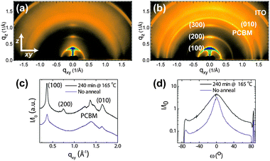 | ||
| Fig. 1 Two-dimensional grazing-incidence X-ray diffraction images of P3HT/PCBM films (a) not annealed and (b) annealed at 165 °C for 240 min. The films were cast on PEDOT∶PSS/ITO to resemble the structure of the active layer in solar cells. (c) In-plane radial traces of GIXD data from (a) and (b) taken at qz = 0.1 Å−1. The data from the annealed film are shifted along the y-axis for comparison. (d) Full pole figures of the same P3HT/PCBM films as a function of the polar angle, ω. | ||
We can obtain a quantitative estimate of the P3HT crystallinity by constructing full pole figures from a combination of GIXD and X-ray rocking experiments as shown in Fig. 1d.11,12 From the pole figure analysis, we have determined the crystallinity of P3HT to be 3-fold higher in the P3HT/PCBM film that was annealed at 165 °C for 240 min compared to that of the unannealed film. We also estimated the P3HT crystallinity of P3HT/PCBM films prepared under a wide range of conditions using the same pole figure analysis. Films of P3HT and PCBM, for example were thermally annealed for 5, 10, 30 or 240 min at 50, 130 or 165 °C. These films were prepared on ITO, as well as ITO pre-treated with n-tetradecylphosphonic acid (HSAM), 1H,1H,2H,2H-perfluorotetradecylphosphonic acid (FSAM), or pre-coated with PEDOT∶PSS to simulate the active layers that are deposited on different anodes in conventional solar cells. Altogether, 19 different processing conditions were explored. Given the strong dependence of the device JSC on the morphology of the active layer,6–9 we have chosen to compare the P3HT and PCBM scattered intensity to the device JSC.
In Fig. 2, we have compiled the extracted JSC of all tested devices as a function of the integral of the product of the full pole figure (Fig. 1d) and sin(ω) over all orientations. This quantity is proportional to the P3HT crystallinity. The JSC varies between 4 to 10 mA cm−2 across all device processing conditions we explored. Consistent with prior reports,8,9 devices with unannealed active layers having low P3HT crystallinities generally exhibit JSC that are markedly lower than those of devices with annealed active layers. We do not, however, observe a definitive correlation between the P3HT crystallinity and the device JSC that encompasses all of our samples. In particular, Fig. 2 emphasizes that while the P3HT crystallinity is important in determining JSC in many of our samples, it is not the only structural property that influences JSC. In what follows, we have quantified our X-ray data to elucidate how the structural development of PCBM influences device JSC.
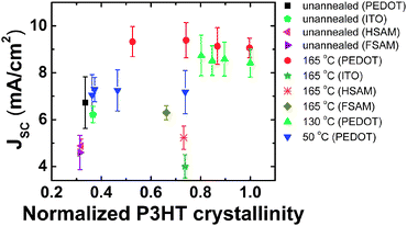 | ||
| Fig. 2 Device JSCvs. normalized P3HT crystallinity of films annealed at 50, 130 or 165 °C for 0, 5, 10, 30 or 240 min. The substrate or anode used was either PEDOT∶PSS (PEDOT), ITO, HSAM or FSAM. The P3HT crystallinity is normalized by the largest P3HT crystallinity found in our samples. Error bars denote standard deviations obtained from multiple experiments. | ||
To fully capture the structural development of PCBM, we should ideally construct full pole figures by stitching the GIXD data with the appropriate rocking scans at the PCBM reflection (q = 1.4 Å−1). The acquisition of rocking curves at q = 1.4 Å−1, however, requires a relatively large X-ray incident angle of 6.2° (for λ = 0.975 Å). At such angles, the X-rays penetrate deep into the specimen, increasing the background contribution to the X-ray diffraction data, which introduces large uncertainties to the diffracted intensity from the organic thin film. To obviate these problems, we opted to only utilize GIXD data to obtain the PCBM scattered intensity by first normalizing the GIXD intensity of the PCBM reflection at 1.4 Å−1 against that of the P3HT (100) reflection acquired during the same scan. This normalization allows us to account for differences in scattered intensities due to small changes in the incident angle during GIXD experiments and enables a meaningful comparison across all samples. For further details, see discussion in the ESI‡. Fig. 3 shows the device JSC as a function of the extracted PCBM scattered intensity for organic solar cells processed with HSAM-treated, FSAM-treated and PEDOT–PSS-coated anodes, as well as those thermally annealed at different temperatures for varying times. As in Fig. 2, the integrated scattered intensity is normalized by the highest PCBM scattered intensity in our samples for ease in comparison. At normalized PCBM scattered intensity of 0.6 or less, JSC of devices comprising these films is linearly and positively correlated with the PCBM scattered intensity irrespective of processing history. At normalized PCBM scattered intensity >0.6, JSC appears to be independent of PCBM scattered intensity. Interestingly, P3HT/PCBM cast on PEDOT∶PSS-coated ITO generally exhibits a higher PCBM scattered intensity, and accordingly, these devices exhibit higher JSC's. The reason for this observation is unclear at this point, though variations in the surface roughness and surface energy between ITO, HSAM- and FSAM-treated ITO or PEDOT∶PSS on ITO could lead to differences in the crystallization and aggregation behavior of PCBM (see ESI‡ for more details).
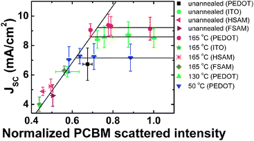 | ||
| Fig. 3 Device JSCvs. normalized PCBM scattered intensity obtained from GIXD of P3HT/PCBM films annealed at 50, 130 or 165 °C for 0, 5, 10, 30 or 240 min. The substrate or anode used was either PEDOT∶PSS (PEDOT), ITO, HSAM or FSAM. The PCBM scattered intensity is normalized by the largest PCBM scattered intensity in our samples. The lines are guides to the eye. Error bars denote standard deviations obtained from multiple experiments. | ||
Unlike the operation of organic thin-film transistors in which charge transport occurs along the dielectric surface, charge transport occurs through the thickness of the active layer during organic solar cell operation. Given that charge transport in P3HT is anisotropic and is favored along the π-stacking direction,13,14 the orientation of P3HT crystallites must affect the JSC we measure during device operation. To quantify this structure–function relationship, we examined the extent of out-of-plane π-stacking of P3HT within active layers of our organic solar cells. We estimate the extent of out-of-plane P3HT π-stacking from the intensity of our P3HT rocking curves near ω = 90°. The P3HT intensity is then normalized by the highest value in our samples for comparison. To determine the factors governing device JSC at normalized PCBM scattered intensity > 0.6, we plot JSC as a function of the normalized P3HT rocking curve intensity near ω = 90° in Fig. 4. We observe a linear correlation between the P3HT rocking curve intensity near ω = 90°, which is related to the extent of out-of-plane π-stacking, and JSC. In the ESI‡, we also obtain an estimate of the extent of out-of-plane π-stacking from GIXD alone. Similar to the results shown in Fig. 4, we obtain a linear trend between the estimated out-of-plane P3HT π-stacking and JSC.
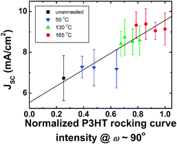 | ||
| Fig. 4 Device JSCvs. normalized P3HT rocking curve intensity at ω = 90°, proportional to the extent of out-of-plane π-stacking of P3HT, from P3HT/PCBM films annealed at various temperatures. The P3HT intensity is normalized by the largest P3HT intensity in our samples. The samples included in this figure have PCBM scattered intensities >0.6. The line is a guide to the eye. Error bars denote standard deviations obtained from multiple experiments. | ||
The operation of polymer solar cells requires efficient hole and electron conduction; one should thus only expect optimal performance when electron and hole transport through the active layer is balanced. Our results in Fig. 3 suggest that establishing local organization of PCBM in the active layer, as evident from the high PCBM scattering intensity, is critical for high-performance P3HT/PCBM devices. On the other hand, when the PCBM local organization in the active layer is sufficiently high (∼0.6 in Fig. 3), and—we postulate—when percolation of PCBM domains throughout the active layer occurs, the device JSC ceases to be sensitive to the local organization of PCBM. Instead, intermolecular hole transport along the π-stacking direction of P3HT13,14 influences device JSC. Careful examination of the GIXD patterns shown in Fig. 1 does in fact suggest the presence of multiple populations of P3HT crystals, from crystals oriented with their (100) planes parallel to the substrate to crystals oriented with their (010) planes parallel to the substrate.
Phase separation of P3HT and PCBM in the active layer can have a strong effect on device performance.8,15–18 The existence of percolating networks with a domain size near the exciton diffusion length (ca. 10 nm)19 is important to prevent recombination losses and promote efficient charge transport.20 Phase separation is notoriously difficult to quantify; while this work does not directly address this phenomenon in P3HT/PCBM active layers, it highlights the structural changes in the active layer that do have strong influences on device performance.
MRSEC funding through Princeton's NSF-sponsored Princeton Center for Complex Materials is acknowledged. Funding from the Sloan Foundation and the Photovoltaics Program at the Office of Naval Research (N00014-08-1-1175) are also acknowledged. Portions of this research were carried out at the Stanford Synchrotron Radiation Lightsource, a national user facility operated by Stanford University on behalf of the U.S. Department of Energy, Office of Basic Energy Sciences. We gratefully acknowledge George Malliaras and Yee-Fun Lim for advice with the initial set up of our solar cell testing facilities, Brad Olsen and Shong Yin for providing Igor routines and codes for X-ray data reduction, and Jeffrey Schwartz for providing the phosphonic acid molecules.
Notes and references
- B. C. Thompson and J. M. J. Frechet, Angew. Chem., Int. Ed., 2008, 47, 58–77 CrossRef.
- R. Kroon, M. Lenes, J. C. Hummelen, P. W. M. Blom and B. de Boer, Polym. Rev., 2008, 48, 531–582 Search PubMed.
- M. C. Scharber, D. Wuhlbacher, M. Koppe, P. Denk, C. Waldauf, A. J. Heeger and C. L. Brabec, Adv. Mater., 2006, 18, 789–794 CrossRef CAS.
- H. Hoppe and N. S. Sariciftci, Adv. Polym. Sci., 2008, 214, 1–86 CAS.
- G. Li, V. Shrotriya, Y. Yao, J. S. Huang and Y. Yang, J. Mater. Chem., 2007, 17, 3126–3140 RSC.
- G. Li, V. Shrotriya, J. S. Huang, Y. Yao, T. Moriarty, K. Emery and Y. Yang, Nat. Mater., 2005, 4, 864–868 CAS.
- H.-Y. Chen, H. Yang, G. Yang, S. Sista, R. Zadoyan, G. Li and Y. Yang, J. Phys. Chem. C, 2009, 113, 7946–7953 CrossRef CAS.
- C. W. Chu, H. C. Yang, W. J. Hou, J. S. Huang, G. Li and Y. Yang, Appl. Phys. Lett., 2008, 92, 103306 CrossRef.
- T. Erb, U. Zhokhavets, G. Gobsch, S. Raleva, B. Stuhn, P. Schilinsky, C. Waldauf and C. J. Brabec, Adv. Funct. Mater., 2005, 15, 1193–1196 CrossRef CAS.
- J. B. Kim, S. S. Lee, M. F. Toney, Z. Chen, A. Facchetti, Y. S. Kim and Y. L. Loo, Chem. Mater., 2010, 22, 4931 CrossRef CAS.
- J. L. Baker, L. H. Jimison, S. Mannsfeld, S. Volkman, S. Yin, V. Subramanian, A. Salleo, A. P. Alivisatos and M. F. Toney, Langmuir, 2010, 26, 9146–9151 CrossRef CAS.
- L. H. Jimison, A. Salleo, M. L. Chabinyc, D. P. Bernstein and M. F. Toney, Phys. Rev. B: Condens. Matter Mater. Phys., 2008, 78, 125319 CrossRef.
- H. Sirringhaus, P. J. Brown, R. H. Friend, M. M. Nielsen, K. Bechgaard, B. M. W. Langeveld-Voss, A. J. H. Spiering, R. A. J. Janssen, E. W. Meijer, P. Herwig and D. M. de Leeuw, Nature, 1999, 401, 685–688 CrossRef CAS.
- L. H. Jimison, M. F. Toney, I. McCulloch, M. Heeney and A. Salleo, Adv. Mater., 2009, 21, 1568–1572 CrossRef CAS.
- C. R. McNeill, S. Westenhoff, C. Groves, R. H. Friend and N. C. Greenham, J. Phys. Chem. C, 2007, 111, 19153–19160 CrossRef CAS.
- V. D. Mihailetchi, H. X. Xie, B. de Boer, L. M. Popescu, J. C. Hummelen, P. W. M. Blom and L. J. A. Koster, Appl. Phys. Lett., 2006, 89, 012107 CrossRef.
- Y. Yao, J. H. Hou, Z. Xu, G. Li and Y. Yang, Adv. Funct. Mater., 2008, 18, 1783–1789 CrossRef CAS.
- J. Peet, J. Y. Kim, N. E. Coates, W. L. Ma, D. Moses, A. J. Heeger and G. C. Bazan, Nat. Mater., 2007, 6, 497–500 CrossRef CAS.
- P. Peumans, A. Yakimov and S. R. Forrest, J. Appl. Phys., 2003, 93, 3693–3723 CrossRef CAS.
- P. K. Watkins, A. B. Walker and G. L. B. Verschoor, Nano Lett., 2005, 5, 1814–1818 CrossRef CAS.
Footnotes |
| † This article is part of the ‘Emerging Investigators’ themed issue for ChemComm. |
| ‡ Electronic supplementary information (ESI) available: Methods and X-ray data and analysis. See DOI: 10.1039/c0cc02927k |
| This journal is © The Royal Society of Chemistry 2011 |