Rapid prototyping of polymeric electrophoresis microchips with integrated copper electrodes for contactless conductivity detection
Wendell Karlos
Tomazelli Coltro
*ab,
José Alberto
Fracassi da Silva
bc and
Emanuel
Carrilho
bd
aInstituto de Química, Universidade Federal de Goiás, Campus Samambaia, 74001-970, Goiânia, GO, Brazil. E-mail: wendell@quimica.ufg.br; Fax: +55 62 3521-1127
bInstituto Nacional de Ciência e Tecnologia de Bioanalítica, Campinas, SP, Brazil
cInstituto de Química, Universidade Estadual de Campinas, 13083-970, Campinas, SP, Brazil. E-mail: fracassi@iqm.unicamp.br
dInstituto de Química de São Carlos, Universidade de São Paulo, 13566-970, São Carlos, SP, Brazil. E-mail: emanuel@iqsc.usp.br
First published on 4th November 2010
Abstract
A simple and easy approach to produce polymeric microchips with integrated copper electrodes for capacitively coupled contactless conductivity detection (C4D) is described. Copper electrodes were fabricated using a printed circuit board (PCB) as an inexpensive thin-layer of metal. The electrode layout was first drawn and laser printed on a wax paper sheet. The toner layer deposited on the paper sheet was thermally transferred to the PCB surface working as a mask for wet chemical etching of the copper layer. After the etching step, the toner was removed with an acetonitrile-dampened cotton. A poly(ethylene terephthalate) (PET) film coated with a thin thermo-sensitive adhesive layer was used to laminate the PCB plate providing an insulator layer of the electrodes to perform C4D measurements. Electrophoresis microchannels were fabricated in poly(dimethylsiloxane) (PDMS) by soft lithography and reversibly sealed against the PET film. These hybrid PDMS/PET chips exhibited a stable electroosmotic mobility of 4.25 ± 0.04 × 10⁻⁴ V cm−2 s−1, at pH 6.1, over fifty runs. Efficiencies ranging from 1127 to 1690 theoretical plates were obtained for inorganic cations.
Introduction
Microchip-based capillary electrophoresis (MCE) has emerged as a powerful and reliable analysis platform. MCE presents several noticeable advantages such as portability, reduced cost and waste, disposability and the potential for on-site use.1–5 MCE devices have been often fabricated in glass and silicon due to their similarities to the fused silica capillaries employed in conventional capillary electrophoresis.6–8 The fabrication of these devices is laborious and it requires sophisticated and expensive instrumentation located in clean rooms.6–8 For this reason, the use of alternative platforms, such as polymer,9 toner10 or paper-based10,11 devices, has offered great opportunities for researchers in this field.Interest in the development of polymeric electrophoresis microdevices has presented continuous growth in recent years. Polymeric substrates offer infinite advantages over pioneered substrates, such as low cost, ease of fabrication, biocompatibility, and high flexibility. A wide range of polymeric substrates and different fabrication protocols have been reported and well-reviewed in the literature.12–19 Among all polymeric materials, PDMS is the most popular substrate explored in microfluidics.15,16 PDMS is elastomeric, inexpensive, and possesses good optical clarity. It also presents reversibly or irreversibly self-sealing capabilities, as well as sealing to other flat surfaces, without distortion of the channels.16
Electrochemical (EC) detection is quite compatible with miniaturization because microelectrodes can be also fabricated using photolithographic procedures. Due to this compatibility, separation channels and detection electrodes can be incorporated together into a single device leading to a fully integrated injection/separation/detection system.20–23 In the last decade, conductivity detection has received considerable attention for coupling with MCE.21,22 Conductivity detection involves a two-electrode system in which electrodes are either in direct contact with the background electrolyte solution (contact mode) or are externally and capacitively coupled to the solution (contactless). Capacitively coupled contactless conductivity detection (C4D) for capillary and microchip electrophoresis has gained much popularity because of its many advantages over the contact mode.21–26 The contactless mode significantly simplifies construction and eliminates interference by the high voltages applied for electrophoretic separation.21,22 Once the electrodes are not in direct contact with the electrolyte within the microchannel, the background noise is greatly decreased leading to lower limits of detection. In addition, problems related to electrode fouling or electrolytic reactions associated with the contact mode are also avoided.20–26
The integration of planar electrodes for contactless conductivity detection on electrophoresis microchips is quite attractive since these devices can be used for applications in this field. Electrodes for on-chip C4D measurements have been often fabricated by sputtering27–29 and screen-printed30 techniques as well as using silver paint,31 aluminium foil32–34 or copper adhesive35,36 strips. The use of copper adhesive or aluminium foil strips compromises chip-to-chip repeatability and prevents the study of more complex geometries. On the other hand, the use of standard techniques such as a sputtering system is quite restricted to a few workplaces due to its high-cost instrumentation. For this reason, research for alternative microfabrication technologies for rapid prototyping of microchips or microelectrodes is the focus of many research groups.
This report describes a simple approach to fabricate a polymeric electrophoresis device coupled with copper electrodes for C4D measurements using easily accessible instrumentals. The copper electrodes were fabricated on a PCB containing a thin copper layer. The detection electrodes were insulated from contact with the channel solution by a PET film coated with a thermo-sensitive adhesive layer. PDMS channels were fabricated by soft lithography and reversibly sealed against the PET surface. Some electrophoresis features, such as electroosmotic flow (EOF), separation performance and run-to-run as well as chip-to-chip repeatability, were investigated.
Experimental
Materials, reagents and samples
The following materials and chemicals were used as received: PCB substrates with single-side copper layer (thickness of 30 µm) (Pinhé, São Carlos-SP, Brazil), waxed paper sheet (Ferragini, Sao Carlos-SP, Brazil, http://www.ferragini.com.br/), Sylgard 184 (Dow Corning, Campinas-SP, Brazil), toner cartridge C4096A (Hewlett Packard, Palo Alto-CA, USA), sodium chloride, potassium chloride, lithium chloride, L-histidine (His) and 2-(N-morpholino)ethanesulfonic acid (MES) (Sigma, St Louis, MO, USA). The 20 mmol L−1MES/His solution (pH = 6.1) was prepared in ultrapure water (resistivity 18 MΩ cm) and filtered through 0.45 µm membrane filters before use. Stock solutions of cations (10 mmol L−1) were prepared in water from the corresponding chloride salts. The working sample solution was prepared daily in running buffer.Fabrication of the copper electrodes
The detection electrodes were fabricated on a commercially available PCB containing a single copper layer (I) as depicted in Fig. 1. The copper surface was previously etched in a 5![[thin space (1/6-em)]](https://www.rsc.org/images/entities/char_2009.gif) :1:7 (v/v/v) H2SO4/H2O2/H2O solution at 55 °C for 30 min. The etching rate was around 0.55 µm min−1. The resulting copper layer thickness was 15 µm. Following this first etching step, the copper surface was polished in order to remove an oxide layer formed due to exposure to air. It was observed that this procedure improved the adherence between the toner layer and the metal surface. The design of the electrode geometry was drawn using Corel Draw 11.0 software (Corel Corporation, Ottawa, Canada) and printed on an A4-size waxed paper sheet by a 1200 dpi resolution laser printer (Hewlett Packard, LaserJet P1005 model). The printed layout was thermally transferred from the paper to the copper surface at 130 °C for 2 min assisted by a pressure of ca. 0.1 MPa (II), similar to the description for toner transfer to a glass surface.37,38 After thermal transference, the unprotected copper layer was chemically etched in a ferric chloride solution for 5 min at room temperature (III). Then, the toner layer was removed by wiping the PCB board with an acetonitrile-dampened cotton, obtaining toner-free copper electrodes (IV). The substrate was rinsed thoroughly with deionized water and dried with N2.
:1:7 (v/v/v) H2SO4/H2O2/H2O solution at 55 °C for 30 min. The etching rate was around 0.55 µm min−1. The resulting copper layer thickness was 15 µm. Following this first etching step, the copper surface was polished in order to remove an oxide layer formed due to exposure to air. It was observed that this procedure improved the adherence between the toner layer and the metal surface. The design of the electrode geometry was drawn using Corel Draw 11.0 software (Corel Corporation, Ottawa, Canada) and printed on an A4-size waxed paper sheet by a 1200 dpi resolution laser printer (Hewlett Packard, LaserJet P1005 model). The printed layout was thermally transferred from the paper to the copper surface at 130 °C for 2 min assisted by a pressure of ca. 0.1 MPa (II), similar to the description for toner transfer to a glass surface.37,38 After thermal transference, the unprotected copper layer was chemically etched in a ferric chloride solution for 5 min at room temperature (III). Then, the toner layer was removed by wiping the PCB board with an acetonitrile-dampened cotton, obtaining toner-free copper electrodes (IV). The substrate was rinsed thoroughly with deionized water and dried with N2.
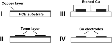 | ||
| Fig. 1 Fabrication of copper electrodes on the printed circuit board (PCB). I, PCB substrate with Cu layer; II, thermally transferred toner mask on Cu surface; III, etching of the Cu layer; and IV, Cu electrodes after removal of the toner. | ||
The electrical insulation between the Cu electrodes and the microfluidic channels was provided by a PET film coated with a thin layer of a thermo-sensitive adhesive, as shown in Fig. 2. A PET film (Fig. 2A) with access holes to electrical connections (i) was cut with dimensions similar to the electrode plate (Fig. 2B). Then, the PET film was put over the PCB substrate. Both pieces were aligned, heated and pressed at 130 °C for 2 min. During the heating, the adhesive layer melts onto the surface, providing a strong seal between the PET film and the PCB substrate, through which the insulated electrodes are obtained (Fig. 2C). The electrodes were designed, in an antiparallel configuration to minimize the stray capacitance, and aligned across the separation microchannel. The electrode dimensions were 20 mm length, 1.0 mm width and 750 µm gap between them.
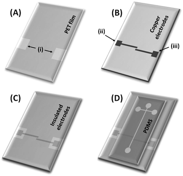 | ||
| Fig. 2 Scheme of the electrical insulation and integration of electrodes to the polymeric channels. (A) PET film with access holes (i) to electrical connections; (B) PCB substrate containing copper electrodes; (C) Cu-electrodes insulated by a PET film after heating (130 °C, 2 min); and (D) assembling of PDMS channels to insulated electrodes for C4D measurements. In (B), the labels (ii) and (iii) represents the electrodes for excitation and pickup the resulting signal, respectively. | ||
Fabrication of the PDMS microchannels
The fabrication of PDMS microchannels using SU-8 molding has been described in detail previously.39 After curing (70 °C for ∼1 h), the PDMS layer was peeled from the master and reversibly sealed to the PET film bringing the two substrates into conformational contact with one another (Fig. 2D). In this case, hybrid PDMS/PET microfluidic structures were produced. The PET film thickness (250 µm) kept the non-contact mode between the electrodes and the microchannel. The separation and injection channels were 40 mm and 15 mm long, respectively. The effective length of the separation channel was 35 mm. The channels were 12 µm deep and 150 µm wide.Electrophoresis procedures
All experiments were performed at room temperature. PDMS/PET channels were first preloaded with isopropyl alcohol to avoid the formation of bubbles. Then, channels were preconditioned with 0.1 mol L−1sodium hydroxide and buffer solution for 5 min each. All solution reservoirs were filled with the same volume (50 µL). Electrokinetic injection was carried out by applying a potential (+750 V) for 8 s to the sample reservoir with the sample waste reservoir grounded and all other reservoirs floating. Electrophoretic separations were performed by switching the high voltage contacts and applying the corresponding separation voltages to the running buffer reservoir with the detection reservoir grounded and all other reservoirs floating. Injection and separation voltages were generated using a bipolar high-voltage power supply (CZE 1000R, Spellman, Hauppauge, New York, USA).Contactless conductivity detection
The separations were monitored by a lab-made C4D system.29 Detection was carried out by passing a sinusoidal excitation signal of 300 kHz and 5 Vpp from the function signal generator to the first electrode and collecting the resulting signal at the second electrode. The C4D data acquisition was carried out using LabVIEW® software. This software was also used to control the injection/separation steps. Electropherograms and the current plot were recorded using a time resolution of 50 ms without software or hardware filtering.Results and discussion
Electrodes fabrication
Preliminary experiments were carried out without the prior etching step, obtaining, in this case, electrodes with ca. 30 µm height. The reversible sealing of PDMS channels against the plate containing the PET-film-coated copper electrodes was not complete due to the formation of air bubbles in the electrode area, also generating channel deformation. In the proposed fabrication process, the channel sealing was similar to that one obtained for hybrid PDMS/glass devices.39 The sealing quality is dependent of the surface cleaning. After decreasing the thickness from 30 to ca. 10–15 µm, the problems related to the sealing of PDMS channels were solved and their integration to the electrodes piece was carried out successfully. Although no fluorescence microscopy experiment was carried out, we can ensure that no leakage was observed. This affirmation is based on the electrical measurements. By monitoring the electrical current, a linear correlation was observed as function of the voltage applied to the channel. By filling the channel with methylene blue, the absence of sample leakage was also assured.The production of electrodes on PCB substrates was monitored by profilometric measurements using a Dektak profilometer model 3 ST (Veeco, Plainview, NY, USA). Fig. 3 shows the profile of two typical copper electrodes on a PCB piece spaced by a 750 µm gap. It is possible to note that the height of both electrodes was ca. 12.5 µm, still presenting a low-roughness surface. It is important to mention that conventional photolithographic technologies could also be used to produce similar copper electrodes on PCB substrates.40,41
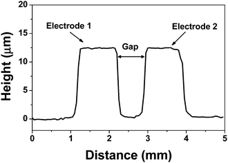 | ||
| Fig. 3 Profile of the copper electrodes fabricated on PCB substrate. | ||
Analytical performance
The analytical performance of the PDMS/PET microchips was evaluated with the separation of inorganic cations including potassium (K+), sodium (Na+) and lithium (Li+). These compounds are often used for evaluating the separation performance in new microfluidic devices with C4D measurements. As can be seen on the electropherograms presented in Fig. 4, the PDMS/PET microchip provided well resolved peaks for an equimolar solution of the cations (200 µmol L−1 each) within less than 30 s.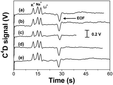 | ||
| Fig. 4 Electropherograms showing the separation of K+, Na+ and Li+ (200 µmol L−1 each) recorded on five (a–e) different hybrid PDMS/PET electrophoresis devices. Running buffer: 20 mmol L−1MES/His, pH 6.1. Injection: 750 V/8 s. Separation: 250 V cm−1. Detection: 300 kHz, 5 Vpp. | ||
The hybrid PDMS/PET devices exhibited excellent repeatability in terms of run-to-run and also chip-to-chip comparison. Fig. 4 shows five electropherograms obtained for the separation of the inorganic cations on five different prototypes. For an inter-chip comparison, the migration times for K+, Na+ and Li+ were 12.2 ± 0.2 s, 14.9 ± 0.1 s and 16.8 ± 0.2 s, respectively. The EOF peak, depicted as a negative peak, presented a migration time of 28.8 ± 0.7 s. Comparing the EOF magnitude for each PDMS/PET device the average value was 4.17 ± 0.10 × 10⁻⁴ cm2 V−1 s−1 with RSD of 2.4%. This low RSD allows concluding that the hybrid PDMS/PET devices demonstrate great potential for routine on-chip applications, in which run-to-run and chip-to-chip repeatability is required. For an intra-chip comparison, the RSD obtained for the EOF (4.25 ± 0.04 × 10⁻⁴ V cm−2 s−1) was 0.9% (n = 50).
The estimated limits of detection (LD) found for inorganic cations ranged from 20 to 30 µmol L−1 (signal-to-noise ratio = 3). When compared to the values reported on polyester-toner (PT) devices,29 the data presented are ca. 10-fold higher. The reason for this discrepancy is attributed to the insulation layer between the detection electrodes and the microfluidic channels. On PT devices, a 100 µm thick transparency provides the physical insulation. For the current device the insulation is accomplished by a 250 µm thick PET film. The LD values can be improved by using a thinner insulation layer as well as by applying high-voltage excitation.40,41
The separation efficiency recorded on hybrid PDMS/PET devices ranged from 1127 to 1690 theoretical plates. These values are greater (around 5-fold higher) than those reported for PT devices29 and similar to recent results found with hybrid glass/PDMS chips.42 In both reports,29,42 the same detection system was used. On PT devices, the channel dimensions are defined by a laser printer that selectively deposits a toner layer on a transparency (polyester) film. The resulting toner surface presents a roughness of ca. 1 µm and, consequently, the channel resolution is not regular when compared to glass or PDMS chips. For this reason, it has been found that the poor separation efficiency reported for PT devices is attributed mainly to the analyte interaction to the toner wall. Quantitative studies demonstrated that the toner channel wall contributes to almost 90% of the total variance.39
Conclusions
An easy and rapid approach to fabricate polymeric electrophoresis microchips with copper integrated electrodes for C4D measurements has been successfully accomplished using simple instrumentation and low-cost consumables. The final microdevice, including channels and electrodes, can be obtained in ca. 1.5 hours. The hybrid PDMS/PET devices exhibited a stable EOF with good run-to-run and chip-to-chip repeatability.In terms of cost, two independent groups43,44 have demonstrated the fabrication of low-cost electrodes (US cents per unit) and their integration with microchip-based electrophoresis systems. In both reports, the use of recordable compact discs (CD-R) to fabricate gold electrodes for coupling with PT43 or PDMS44electrophoresis devices was successfully demonstrated. The PCB-based electrodes used in this work are economically attractive alternatives to be used in locations with resource-limited settings or where sputtering facilities are not readily accessible.45,46 We estimated that the cost of each integrated device is ca. two dollars. This approach can become even cheaper and faster with use of a laser-printing step to produce masters for soft-lithography.10
Acknowledgements
This project was supported by CNPq and FAPESP. The authors would like to acknowledge the Microfabrication Laboratory of the Brazilian Synchrotron Light Laboratory for use of their facilities. Dr Carol Collins and Dr Carlos A. Neves are also thanked for manuscript revision and for writing the first version of the software in LabVIEW®, respectively.References
- T. Vilkner, D. Janasek and A. Manz, Anal. Chem., 2004, 76, 3373–3385 CrossRef CAS.
- P. S. Dittrich, K. Tachikawa and A. Manz, Anal. Chem., 2006, 78, 3887–3907 CrossRef CAS.
- W. K. T. Coltro, E. Piccin, E. Carrilho, D. P. de Jesus, J. A. Fracassi da Silva, H. D. T. da Silva and C. L. do Lago, Quim. Nova, 2007, 30, 1986–2000 CAS.
- J. West, M. Becker, S. Tombrink and A. Manz, Anal. Chem., 2008, 80, 4403–4419 CrossRef CAS.
- A. Arora, S. G. Giuseppina, G. B. Salieb-Beugelaar, J. T. Kim and A. Manz, Anal. Chem., 2010, 82, 4830–4847 CrossRef CAS.
- Z. J. Jia, Q. Fang and Z. L. Fang, Anal. Chem., 2004, 76, 5597–5602 CrossRef CAS.
- M. Castaño-Álvarez, D. F. P. Ayuso, M. G. Granda, M. T. Fernandez-Abedul, J. R. Garcia and A. Costa-Garcia, Sens. Actuators, B, 2008, 130, 436–448 CrossRef.
- I. Rodriguez, P. Spicar-Mihalic, C. L. Kuyper, G. S. Fiorini and D. T. Chiu, Anal. Chim. Acta, 2003, 496, 205–215 CrossRef CAS.
- H. Becker and C. Gartner, Anal. Bioanal. Chem., 2008, 390, 89–111 CrossRef CAS.
- W. K. T. Coltro, D. P. de Jesus, J. A. F. da Silva, C. L. do Lago and E. Carrilho, Electrophoresis, 2010, 31, 2487–2498 CrossRef CAS.
- A. W. Martinez, S. T. Phillips, G. M. Whitesides and E. Carrilho, Anal. Chem., 2010, 82, 3–10 CrossRef CAS.
- V. Dolník, S. Liu and S. Jovanovich, Electrophoresis, 2000, 21, 41–54 CrossRef CAS.
- H. Becker and C. Gartner, Electrophoresis, 2000, 21, 12–26 CrossRef CAS.
- H. Becker and L. E. Locascio, Talanta, 2002, 56, 267–287 CrossRef CAS.
- D. C. Duffy, J. C. McDonald, O. J. A. Schueller and G. M. Whitesides, Anal. Chem., 2000, 70, 4974–4984.
- J. C. McDonald and G. M. Whitesides, Acc. Chem. Res., 2002, 35, 491–499 CrossRef CAS.
- G. S. Fiorini and D. T. Chiu, BioTechniques, 2005, 38, 429–446 CrossRef CAS.
- H. Shadpour, H. Musyimi, J. Chen and S. A. Soper, J. Chromatogr., A, 2006, 1111, 238–251 CrossRef CAS.
- E. Piccin, W. K. T. Coltro, J. A. F. da Silva, S. Claro-Neto, L. H. Mazo and E. Carrilho, J. Chromatogr., A, 2007, 1173, 151–158 CrossRef CAS.
- D. J. Fischer, M. K. Hulvey, A. R. Regel and S. M. Lunte, Electrophoresis, 2009, 30, 3324–3333 CrossRef CAS.
- P. Kubáñ and P. C. Hauser, Anal. Chim. Acta, 2008, 607, 15–29 CrossRef CAS.
- M. Pumera, Talanta, 2007, 74, 358–364 CrossRef CAS.
- R. S. Pai, K. M. Walsh, M. M. Crain, T. J. Roussel, D. J. Jackson, R. P. Baldwin, R. S. Keynton and J. F. Naber, Anal. Chem., 2009, 81, 4762–4769 CrossRef CAS.
- J. G. A. Brito-Neto, J. A. F. da Silva, L. Blanes and C. L. do Lago, Electroanalysis, 2005, 17, 1198–1206 CrossRef CAS.
- J. A. F. da Silva and C. L. do Lago, Anal. Chem., 1998, 70, 4339–4343 CrossRef.
- P. Kubáñ and P. C. Hauser, Electrophoresis, 2009, 30, 176–188 CrossRef CAS.
- J. Lichtenberg, N. F. de Rooij and E. Verpoorte, Electrophoresis, 2002, 23, 3769–3780 CrossRef CAS.
- C. Lee, C. M. Chen, G. Chang, C. Lin and L. Fu, Electrophoresis, 2006, 27, 5043–5050 CrossRef CAS.
- W. K. T. Coltro, J. A. F. da Silva and E. Carrilho, Electrophoresis, 2008, 29, 2260–2265 CrossRef CAS.
- J. Wang, G. Chen, M. P. Chatrathi, M. Wang, R. Rinehart and A. Muck, Electroanalysis, 2008, 20, 2416–2421 CrossRef CAS.
- J. Tanyanyiwa and P. C. Hauser, Anal. Chem., 2002, 74, 6378–6382 CrossRef CAS.
- M. Pumera, J. Wang, F. Opekar, I. Jelinek, J. Feldman, H. Lowe and S. Hardt, Anal. Chem., 2002, 74, 1968–1971 CrossRef CAS.
- J. Wang, G. Chen and A. Muck, Jr, Anal. Chem., 2003, 75, 4475–4479 CrossRef CAS.
- Y. Ding, C. D. Garcia and K. R. Rogers, Anal. Lett., 2008, 41, 335–350 CrossRef CAS.
- C. L. do Lago, H. D. T. da Silva, C. A. Neves, J. G. A. Brito-Neto and J. A. F. da Silva, Anal. Chem., 2003, 75, 3853–3858 CrossRef.
- E. M. Abad-Villar, J. Tanyanyiwa, M. T. Fernandez-Abedul, A. Costa-Garcia and P. C. Hauser, Anal. Chem., 2004, 76, 1282–1288 CrossRef CAS.
- C. L. do Lago, D. P. de Jesus, H. D. T. da Silva, C. A. Neves, J. G. A. Brito-Neto and J. A. F. da Silva, Electrophoresis, 2004, 25, 3825–3831 CrossRef.
- W. K. T. Coltro, E. Piccin, J. A. F. da Silva, C. L. do Lago and E. Carrilho, Lab Chip, 2007, 7, 931–934 RSC.
- W. K. T. Coltro, S. M. Lunte and E. Carrilho, Electrophoresis, 2008, 29, 4928–4937 CrossRef CAS.
- P. Kubáñ and P. C. Hauser, Lab Chip, 2005, 5, 407–415 RSC.
- P. Kubáñ and P. C. Hauser, Lab Chip, 2008, 8, 1829–1836 RSC.
- T. P. Segato, W. K. T. Coltro, A. L. J. Almeida, M. H. O. Piazetta, A. L. Gobbi, L. H. Mazo and E. Carrilho, Electrophoresis, 2010, 31, 2526–2533 CrossRef CAS.
- W. K. T. Coltro, J. A. F. da Silva, H. D. T. Silva, E. M. Richter, R. Furlan, L. Angnes, C. L. do Lago, L. H. Mazo and E. Carrilho, Electrophoresis, 2004, 25, 3832–3839 CrossRef CAS.
- D. C. Kirkpatrick, C. Antwi and R. Scott Martin, Anal. Methods, 2010, 2, 811–816 RSC.
- M. Abdelgawad and A. R. Wheeler, Adv. Mater., 2007, 19, 133–137 CrossRef CAS.
- M. Vázquez, C. Frankenfeld, W. K. T. Coltro, E. Carrilho, D. Diamond and S. M. Lunte, Analyst, 2010, 135, 96–103 RSC.
| This journal is © The Royal Society of Chemistry 2011 |