Ultrafast studies of single semiconductor and metal nanostructures through transient absorption microscopy
Gregory V.
Hartland
*
Department of Chemistry and Biochemistry, University of Notre Dame, Notre Dame, IN 46556-5670, USA. E-mail: ghartlan@nd.edu; Tel: +1 574 631-9320
First published on 17th June 2010
Abstract
The past decade has seen tremendous progress in the development of absorption based techniques for studying single semiconductor and metal nanoparticles. These techniques complement the more common emission and Rayleigh scattering measurements. The advantages of absorption-based detection are that a wider range of materials can be examined compared to emission, and smaller particles can be studied than is possible with Rayleigh scattering. These advantages are somewhat offset by increased difficulty. Importantly, by employing absorption based detection with a pump and probe beam, transient absorption experiments can be performed on single nanostructures. This allows dynamics measurements on ultrafast (sub-ps) timescales, and is the focus of this mini-review. These experiments provide information about how processes such as electron–phonon coupling, energy dissipation, and charge carrier trapping vary between nanostructures, as well as how they depend on environment.
 Prof. Gregory V. Hartland | Prof. Hartland obtained his B.Sc. (Hons.) degree from the University of Melbourne (Australia) in 1985, and a Ph.D. degree from the University of California, Los Angeles in 1991. He performed postdoctoral research with Prof. Hai-Lung Dai at the University of Pennsylvania, before joining the University of Notre Dame as an Assistant Professor in 1994. He was promoted to Associate Professor in 2000, and Full Professor in 2004. Prof. Hartland’s current research interests are in using optics to study the properties of metal and semiconductor nanostructures, particularly, single particle measurements. He is a member of the Editorial Advisory board of Physical Chemistry Chemical Physics (2005–present) and a Senior Editor of The Journal of Physical Chemistry (2009–present). |
1. Introduction and background
Single particle optical measurements are becoming an increasing important way of investigating the properties of nanomaterials.1–3 There are several motivations for these studies: first, samples of nanomaterials contain a range of different sizes, shapes and even compositions. These differences can affect properties, and to understand this it is important to study individual particles. A good example is the Rayleigh scattering spectra of metal nanoparticles, which vary tremendously with size and shape.4 Second, single particle measurements provide a means of investigating how the particles interact with their surroundings in a more precise way than is possible with ensemble measurements. This is because the local environment is often different for different particles. This sensitivity to environment is at the heart of molecular recognition schemes based on single particle spectroscopy.5,6 Finally, new phenomena can be revealed by single particle experiments. The best-known example is fluorescence intermittency (“blinking”), where emission from a particle (or molecule) turns on and off at seemingly random times.7The time-resolution in single particle measurements is a significant issue for designing experiments. Semiconductor particles are usually studied by emission, and lifetime information can be obtained by time-correlated single photon counting (TCSPC). The time-resolution of single particle TCSPC is limited to a few hundred picoseconds, which is fast enough to study radiative lifetimes,8–11 and to generate information about (slow) electron transfer reactions.12 However, fast picosecond processes such as Auger recombination and charge carrier trapping cannot be studied.13 It is also difficult to study materials with low emission quantum yields by TCSPC.
Single metal nanoparticles can be detected by Rayleigh scattering, using either total internal reflection or dark-field illumination.3,4,14,15 Dispersing the scattered light with a spectrometer allows the width of the plasmon resonance to be measured, which provides information about very fast (femtosecond) electron-surface scattering and radiation damping processes.3,16–18 However, it is not possible to study electron–phonon coupling and energy dissipation,19 which are important for applications such as photo-thermal therapy – where heat dissipation from optically excited metal nanoparticles is used to selectively kill cells.20–22 Rayleigh scattering experiments are also hard to do for particles smaller than ca. 20 nm diameter, because the efficiency is proportional to volume squared, and so dies off quickly with size.2
Many of the disadvantages of Rayleigh scattering and emission detection can be ameliorated using optical absorption to study single particles.2,23 Absorption based measurements are more general than emission (everything that emits absorbs, but the converse is not true), and they allow the study of smaller particles than is possible by Rayleigh scattering.2,24 More importantly, however, by using absorption detection pump–probe measurements can be performed with ultrafast time resolution.25,26 This allows the study of a range of picosecond processes in semiconductor and metal nanoparticles that cannot be interrogated with conventional TCSPC or Rayleigh scattering measurements. These are significant advantages; however, it is obvious that absorption based measurements are more difficult than zero-background techniques like emission and Rayleigh scattering detection.
To understand why absorption detection of single particles works, consider a focused Gaussian beam with an intensity distribution of I(r) = (2P/πw20)e−2r2/w02, where w0 is the beam waist, r is the radial distance from the beam center, and P is total power carried by the beam.27 A particle placed at the center of the beam will experience an intensity of 2P/πw20, and will cause a change in the transmitted power of ΔP/P = −2σ/πw20, where σ is the extinction cross-section of the particle.28 In this expression the geometrical factor of πw20/2 is equal to the area of a uniform “top-hat” beam with the same total power and peak intensity as the Gaussian beam.27 This gives the simple interpretation that the change in transmitted intensity is the cross-section of the particle divided by the area of the laser spot.28 For a 10 nm diameter gold particle and a 532 nm laser focused to a diffraction limited spot σ ≈ 80 nm2 and w0 ≈ λ/NA ≈ 400 nm,27 where NA is the numerical aperture of the objective (which we take as 1.3 for a 100× oil immersion objective). This implies a change in transmitted power of ∼1%. This is a small change, but it can be easily detected with a lock-in amplifier if the signal can be modulated in some way.
There are several methods for extracting the absorption of a single particle from the background. For example, in spatial modulation spectroscopy (SMS),28 the nanoparticle is moved in and out of the laser beam. These measurements directly give the absolute extinction cross-section of the particle, and scanning the laser wavelength yields the extinction spectrum. The combination of spectral and cross-section information allows the size and shape of the particle to be determined solely from optical measurements.28,29 This is an advantage compared to Rayleigh scattering, where it is difficult to determine absolute scattering cross-sections from the intensity.30,31 Another way of detecting small particles via absorption is to monitor the heat deposited in the sample using a non-resonant probe.23,32 This technique is known as photothermal heterodyne imaging (PHI), and is very sensitive: the spectra of 5 nm diameter Au particles have been recorded using PHI.33 However, PHI does not give absolute extinction cross-section information, which is a disadvantage compared to SMS.
In pump–probe transient absorption experiments the change in the probe intensity induced by the pump is monitored. This is done by chopping the pump and recording the difference in signal between the pump-on and pump-off. For single particle measurements the magnitude of the signal is ΔP/P = −2Δσ/πw20, where Δσ is the change in cross-section of the particle caused by the pump laser.26 Very low pump intensities must be used in these experiments to avoid destroying the particles: typically the pump powers are on the order of pJ/pulse. This means that Δσ is very small: the detected signal is at least two orders of magnitude smaller than the straight absorption signal. Thus, very stable laser sources and sensitive detection techniques are needed.
These experiments were first performed by Orrit and co-workers using a birefringent crystal to create perpendicularly polarized signal and reference beams in a common path interferometer.25 This scheme provides shot-noise limited detection, and allows the absorptive and dispersive contributions to the signal to be separately extracted.34 Orrit and co-workers used this instrument to examine the response of single gold nanoparticles to ultrafast excitation. In transient absorption experiments on metal particles the pump laser deposits energy into the electron distribution.19 Redistribution of the energy between the electrons and phonons creates a rapid increase in lattice temperature, which coherently excites vibrational modes of the particle that correlate with the expansion co-ordinate (primarily the breathing mode).19,35–37 This effect shows up as an oscillating signal in the transient absorption traces. Ensemble measurements provide information about how the vibrational frequencies depend on size and shape, but they do not give any meaningful information about damping.36 This is because different size particles have different frequencies, and adding the contributions from all the particles in the sample leads to an inhomogeneous decay. This averaging can be removed by single particle measurements. In their initial publication the Orrit group showed that the vibrational lifetimes of single gold nanoparticles are four to five times longer than the decay for an ensemble.25 They subsequently examined single gold nanorods38 and dumbbell shaped particles,39 providing precise information about the acoustic vibrational frequencies and energy relaxation of these materials.
Soon after the initial report by the Orrit group, the group of Vallee and Del Fatti reported transient absorption measurements for single silver nanoparticles based on a straightforward optical pump–probe scheme.26 While sacrificing some of the sensitivity of the common path interferometer, this scheme is much easier to set up. By using a high repetition rate laser, single particles with dimensions in the order of 20 nm can be easily detected with high signal-to-noise. Their initial reports examined electron–phonon coupling in single Ag and Au particles.26,40 They have also investigated the vibrational dephasing of Au nanoparticle dimers produced by nanosphere lithography.41 A large variation in the lifetimes of the acoustic vibrational modes was observed, which was attributed to differences in coupling to the substrate for different dimers.
Ultrafast pump–probe single particle measurements have also been performed using Rayleigh scattering detection for metals,42,43 and fluorescence detection or second harmonic generation for semiconductors.44–47 These techniques are less general than the transient absorption microscopy experiments described below, as they are limited to materials that either emit or scatter strongly, or that posses a non-centrosymmetric crystal structure.44 In the following, I will describe how single particle transient absorption microscopy experiments are performed in my laboratory, and give example results from metal nanoparticles,48 and metal49,50 and semiconductor nanowires51 that illustrate the utility of this technique.
2. Transient absorption microscopy
A diagram of the optical system used for transient absorption microscopy is show in Fig. 1. This instrument is based on the scheme of Del Fatti and Vallee.26 The beam from a Ti:Sapphire oscillator is split to provide the pump and probe pulses, with one of the beams being frequency doubled in a non-linear optical crystal. The intensities of the beams are controlled by λ/2-waveplate/polarizer combinations and neutral density filters. The pump is chopped at high frequency with an acousto-optic modulator (AOM), and the relative timing of the beams is controlled by a stepper-motor driven translation stage. The pump and probe are made co-linear with a dichroic beamsplitter, and focused at the sample with a high NA oil immersion objective. The beams are re-collimated after the sample with a second high NA oil immersion objective, and the pump is extinguished using a combination of optical filters. The probe is then detected with an avalanche photodiode (APD). An APD is needed because very low intensity probe pulses (<0.1 pJ/pulse) must be used. The output of the APD is sent to a lock-in amplifier referenced to the AOM.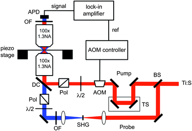 | ||
| Fig. 1 Diagram of the experimental apparatus for transient absorption microscopy. APD = avalanche photodiode; OF = optical filters used to extinguish the Ti:Sapphire fundamental; BS = beam-splitter; DC = dichroic beam-splitter; TS = translation stage; Pol = polarizer; λ/2 = half-waveplate; AOM = acousto-optic modulator; SHG = second harmonic generation crystal. The diagram is drawn for a near-IR pump and near-UV probe, but the instrument can be easily implemented the other way around. | ||
In our experience, all the optical elements given in Fig. 1 are essential to the success of the experiment. Samples are typically prepared by spin coating a dilute polyvinyl-alcohol solution of the nanoparticles onto a clean glass coverslip. Transient absorption traces are collected by changing the relative delay between the pump and probe beams with the translation stage, and images are collected by raster scanning the sample with respect to the laser focus using a closed loop piezo-stage. The transient absorption traces typically contain a background signal, which is attributed to thermal lensing.23,32 This signal has been subtracted from the traces for the data presented below. Note that the experimental technique described in this mini-review is essentially the same as the stimulated emission microscopy technique described by Xie and co-workers.52 However, our emphasis is on dynamics studies of nanomaterials, rather than imaging biological systems.
3. Results and discussion
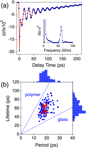
Fig. 2(a) and (b) show single particle and ensemble transient absorption traces for a silver nanocube sample with an average edge length of 35.5 ± 3.4 nm.48 The single particle measurements were performed with 880 nm pump pulses and 440 nm probe pulses (this probe wavelength is close to the plasmon resonance of the particles). The single particle and ensemble traces have a similar form: they both show a fast decay due to electron–phonon coupling followed by modulations from the coherently excited breathing mode.19,35 However, the modulations are much better defined and have a longer lifetime in the single particle trace.25,48 The inset in Fig. 2(a) shows the Fourier transform of the modulated portion of the single particle trace, which gives the frequency of the breathing mode. The vibrational lifetime was determined by fitting the data to a damped cosine function, with the frequency fixed to the value determined from the Fourier transform (the fit is shown as the red line in Fig. 2(a)).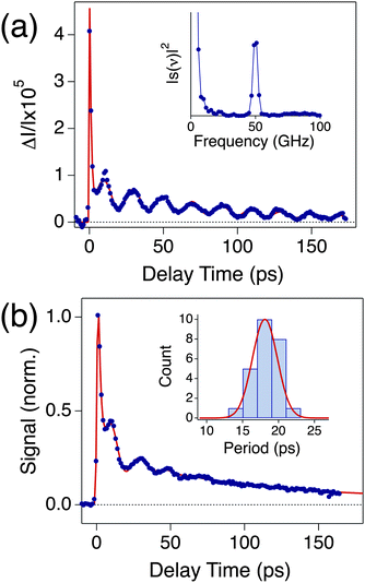 | ||
| Fig. 2 (a) Transient absorption trace from a single Ag nanocube from a sample with an average edge length of 35.5 ± 3.4 nm. The inset shows the Fourier transform of the modulated portion of the data. (b) Ensemble transient absorption trace for the Ag nanocube sample. The inset of (b) gives a histogram of the measured periods from the single particle experiments. The red line is the distribution calculated from the size distribution of the sample. Reproduced with permission from the ACS from ref. 48. | ||
A total of 25 particles were examined in these experiments, and the average frequency was 53.8 ± 4.9 GHz (error equals standard deviation). This is consistent with the result of the ensemble measurement, which gave νbr = 52.3 ± 2.7 GHz (error equal to standard error). The average lifetime of the breathing mode from the single particle experiments was 57.6 ± 7.4 ps, which is approximately two times longer than the dephasing time for the ensemble measurement.48 This difference is entirely due to removing the inhomogeneous damping from the distribution of sizes.
The inset of Fig. 2(b) shows a histogram of the measured periods, along with a curve that represents the distribution expected from the known size distribution of the sample (periods are plotted rather than frequencies, as the period is directly proportional to the dimensions of the particle). The curve was calculated using the continuum mechanics expression for the breathing mode period of 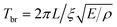 , where L is the edge length, ξ is the reduced frequency of the breathing mode, and E and ρ are the Young's modulus and density of the material.53 The excellent match between the measured histogram and the calculated curve shows that the distribution of periods in the single particle experiments simply comes from the distribution in sizes in the sample.48 Thus, the substrate has little effect on the vibrational period. However, it is not clear whether this is true for the damping times. In these measurements the vibrational damping times and periods are expected to be strongly correlated, as they scale with dimensions in the same way.54 The silver nanocube data shows very little correlation between the period and damping time. This implies that the damping times are affected by the environment, and that there is significant heterogeneity in the local environment.41,48,49
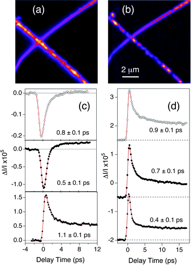
One of the problems in these experiments is finding the particles, and ensuring only one particle is at the focus of the microscope. This is very time-consuming and limited the number of particles that could be studied in the silver nanocube experiments described above. On the other hand, metal nanowires are much easier to find under the microscope, as they are very bright in Rayleigh scattering.49,55,56 The contrast in the Rayleigh scattering images can also be used to determine whether the object is a single wire or multiple wires. A scattered light image of two silver nanowires is shown in Fig. 3(a).49 This image was taken with a camera that automatically subtracts the background. However, metal nanowires with diameters greater than 20 nm can be easily seen by eye when epi-illuminated by a white light source. Fig. 3(b) shows an image where the near-IR pump laser has been focused at one end of the kinked nanowire in Fig. 3(a). This excites propagating surface plasmon polariton (SPP) modes of the wire.55–58 These are electronic excitations that travel down the wire, but only couple to light at the ends or discontinuities in the wire due to momentum matching considerations.55–58 This can be clearly seen in Fig. 3(b).
 | ||
| Fig. 3 (a) Scattered light image of two silver nanowires. (b) Image recorded with the near-IR pump laser focused at the end of the kinked wire in (a). Light emission occurs at points in the wire where there is a break in cylindrical symmetry. (c) Transient absorption image (9 × 14 μm image size) of two Ag nanowires recorded with temporally and spatially overlapped pump and probe pulses. (d) Polarization dependence of the transient absorption signal for a different Ag nanowire. Red = near-IR pump, and blue = near-UV probe. The signal is maximized when the pump is aligned along the nanowire axis, and the probe is perpendicular to the axis. Figures 3(a) and (b) reproduced with permission from Wiley-InterScience from ref. 49, Figure 3(c) and (d) reproduced with permission from the RSC from ref. 50. | ||
Fig. 3(c) shows a transient absorption image of two different silver nanowires. This image was collected with temporally and spatially overlapped pump and probe pulses, with wavelengths of 860 nm and 430 nm, respectively.50 There are several points to note about this image. First, the signal at the end of the wires is stronger than in the middle. This is because the pump laser can excite the propagating SPP modes at the wire ends and, therefore, couple more energy into the electron distribution.55–58 Second, the longer wire in Fig. 3(c) shows different signal levels in different regions of the image. This arises because the signal depends on the alignment of the laser polarizations with the nanowire axis,57,58 and the bend in the longer wire causes a miss-alignment in the lower right region of the image.50
A plot of the magnitude of the transient absorption signal versus the polarization of the pump and probe beams is shown in Fig. 3(d) for a silver nanowire which was almost horizontal in the sample plane (∼−15° angle). The signal is maximized when the polarization of the near-IR pump laser is parallel to the nanowire axis, and the near-UV probe is perpendicular to the nanowire. The same polarization dependence is seen independent of whether the nanowire is excited in the middle or at the ends.50 This is consistent with the near-UV probe being resonant to the transverse plasmon mode,59 and the near-IR pump exciting propagating SPP modes57 and/or antenna modes of the wire.58,60 The transient absorption image in Fig. 3(c) shows that the propagating SPP modes and the antenna modes have similar absorption strengths. This is fundamental information about how metal nanowires couple to light, that has not been seen in previous studies of these materials.
Fig. 4(a) shows a transient absorption trace for one of the silver nanowires examined in this work. Like the nanocube results, the signal shows a fast decay corresponding to electron–phonon coupling, followed by modulations due to the breathing mode.50 A Fourier transform of the modulated portion of the data is presented in the inset of Fig. 4(a). The vibrational frequencies for the nanowires are similar to those for the nanocubes, however, the signal is much larger. The magnitude of the transient absorption signal is proportional to the effective volume probed in the experiments, and there are two important factors. First, the dimensions of the nanowires in these experiments are larger than those of the nanocubes (61.9 ± 11.2 nm diameter for the nanowires versus 35.5 ± 3.4 nm edge length for the cubes). Second, in the nanowire experiments, the effective volume probed is the cross-sectional area of the wire times the diameter of the laser spot ( ), whereas for the nanocubes it is the volume of the particle (edge length cubed L3). These differences in dimensions and experimental geometry give about a factor of ten difference in the effective volume interrogated in the experiments, which is consistent with the difference in signal levels between Fig. 2 and 4.
 | ||
| Fig. 4 (a) Transient absorption trace for a single Ag nanowire. The inset shows the Fourier transform of the modulated portion of the data. The red line is a fit to the data using an exponential decay for the early time signal, and a damped cosine for the modulations. (b) Lifetime versus period data for the Ag nanowires (blue dots) and Ag nanocubes (red squares) examined in ref. 48 and 50. The lines represent the vibrational lifetimes expected for Ag particles in a glass or polymer environment. The histograms on the axes correspond to the nanowire data. | ||
Fig. 4(b) shows a plot of the vibrational lifetimes versus the period for the silver nanowires and nanocubes examined in these experiments. There are many more data points for the nanowires, simply because it is much easier to find the wires under the microscope. The lines in Fig. 4(b) are calculated values of the lifetime versus period for silver nanoparticles in glass and polymer environments (the samples are prepared by spin coating a polymer solution onto a glass substrate).49,50,54 The calculations were performed using an analytic model for the damping of the breathing mode of a sphere in a homogeneous solid.54,61 Even though our particles are not spherical, we believe that these calculations should catch the essential physics of the damping.50 The calculations show that the lifetime of the breathing mode depends strongly on the difference in acoustic impedance (Z = ρcl) of the particle and its surroundings. When the acoustic impedance difference is small, acoustic energy flows rapidly from the particle into the surroundings, giving strong damping. In contrast, when there is a large difference in acoustic impedances, the energy remains inside the particle and the damping times are much longer. Glass has a larger acoustic impedance than polymer and, therefore, a smaller acoustic impedance mismatch with silver. This causes stronger damping of the acoustic vibrational modes of the silver nanoparticles for a glass environment.49,50
The experimental data points are bounded by the calculations. This leads to the following picture of the breathing mode dynamics: nanoparticles (cubes or wires) that are in close contact with the glass support have short damping times, whereas nanoparticles in the polymer have long damping times. The majority of the nanoparticles feel environments that are in-between glass and polymer. The heterogeneity in the local environment experienced by the nanoparticles causes the spread in the lifetime measurements. This is also reflected in the correlation between the periods and damping times. The data for the nanowires shows a medium correlation (correlation coefficient = 0.45), in contrast to the strong correlation expected from theory.50 Information about the effect of local environment on the acoustic mode damping is one of the major outcomes of single particle transient absorption measurements.
We have also used transient absorption microscopy to examine the dynamics of single II–VI semiconductor nanowires.51 A scattered light image of two crossed CdTe nanowires, and the corresponding transient absorption image are shown in Fig. 5(a) and (b), respectively. The transient absorption experiments were performed using 400 nm pump pulses and 800 nm probe pulses. The same features are reproduced in the two images. The roughness in the optical images is attributed to variations in the nanowire thickness.51 These samples were produced by chemical vapor deposition, and have significant intra- and inter-wire diameter variations.62
 | ||
| Fig. 5 (a) Scattered light image of two crossed CdTe nanowires (false color image). (b) Transient absorption image (10 × 10 μm image size) of the same two nanowires recorded with near-UV pump pulses and near-IR probe pulses. (c) Transient absorption traces from different CdTe nanowires. (d) Transient absorption traces recorded at different spatial positions along a single CdTe nanowire. The numbers in (c) and (d) represent the time constants for the fast initial decay. The transient absorption data in this figure was collected with circularly polarized pump and probe beams. Reproduced with permission from the ACS from ref. 51. | ||
Transient absorption traces for different single CdTe nanowires are shown in Fig. 5(c). The signal can be either a bleach (positive ΔI/I) or an absorption (negative ΔI/I) in these experiments, depending on the position of the band-edge of the nanowire compared to the probe wavelength. When the band-edge is close to the probe wavelength, a bleach is obtained due to state filling.63 In contrast, when the probe wavelength is red-shifted from the band-edge we see an absorption signal. The red shifted absorption most likely arises from transitions involving a localized hole state.64,65 Shifts in the band-edge for the different nanowires are assigned to Stark effects from trapped charges.66 All the traces for the CdTe nanowires show a fast decay, which is assigned to charge carrier trapping at surface states. The time constant is different for different wires, presumably because of differences in the density and or energies of the surface trap sites.51,67,68
Fig. 5(d) shows transient absorption traces recorded at different spatial positions along a single nanowire (the traces were separated by several microns). The form of the signal is the same for the different traces, which implies that the absorption onset is constant along the length of the nanowire. However, the time constant for the fast decay changes from trace to trace. This shows that the distribution of trap sites varies along the wire. This is consistent with single wire emission studies, which typically show differences in emission quantum yield along the length of the nanowires.69 This is the first time that this type of heterogeneity has been directly observed in ultrafast measurements.
4. Conclusions and outlook
Many processes of interest in nanomaterials occur on times scales of picoseconds to hundreds of picoseconds. This includes electron–phonon coupling in metals,19,35 Auger recombination and charge carrier trapping in semiconductors,13,67,68 heat dissipation,36,70 and dephasing of vibrational resonances.25 The timescales for these processes depend on the size, shape and environment of the nanostructure, which means that single particle experiments are needed to study them effectively. This requires techniques with high spatial and temporal resolution, as well as high sensitivity. One way of doing this is transient absorption microscopy.25,26 This technique is more general than emission or Rayleigh scattering measurements, and can be used to study a wide variety of materials.The systems that have been examined to date using transient absorption microscopy include different shaped Au and Ag nanoparticles,25,26,38–40,48 nanoparticle dimers,41 and nanowires of Ag49,50 and CdTe.51 For metal nanostructures, the main results have been the measurement of the dephasing times of the acoustic vibrational modes.25,38,41,48–50 The dephasing times show significant variation between different particles, which is attributed to heterogeneity in the environment.41,50 Thus, these experiments provide information about how the particles couple to their surroundings. On the other hand, experiments with semiconductor nanostuctures yield information about the timescales for internal charge carrier relaxation.51 For CdTe nanowires both inter- and intra-wire variations in the charge carrier dynamics were seen, presumably due to differences in the surface chemistry of the wires (which affects the energy and density of trap sites).51
The ability to provide information about variations in dynamics between different nanostructures will make transient absorption microscopy an important addition to the nanoscience tool-box in coming years. One of the key issues moving forward is the sensitivity and the detection limit of the technique. The data in Fig. 5 has a signal-to-noise level of ∼100![[thin space (1/6-em)]](https://www.rsc.org/images/entities/char_2009.gif) :1. These wires are approximately 40 nm in diameter, and have an absorption cross-section of σ ≈ 4 × 10⁻¹⁰ cm2 μm−1 at the pump wavelength.51,71 This translates to an effective cross-section of
:1. These wires are approximately 40 nm in diameter, and have an absorption cross-section of σ ≈ 4 × 10⁻¹⁰ cm2 μm−1 at the pump wavelength.51,71 This translates to an effective cross-section of  in our diffraction limited measurements (in experiments with nanowires the effective cross-section depends on the spot size). These experiments were performed with a fixed probe wavelength. Using a tunable laser (for example an optical parametric oscillator) to probe at the band-edge should increase the signal by at least 10 times.62,65 Thus, by exploiting resonance conditions we will be able to interrogate nanostructures with cross-sections of ∼10−12 cm2 with a signal-to-noise level of >10:1 without any improvement in laser stability. For II–VI nanowires, this implies nanowires with diameters of ∼4 nm should be amenable to study. Improvements in laser stability over our current home-built system will allow even smaller objects to be investigated.
Acknowledgements
This work has been supported by the National Science Foundation through Grant CHE-0647444, and by the University of Notre Dame Faculty Research Program. The silver nanocube and nanowire experiments described in this mini-review were performed by Hristina Staleva, and the CdTe nanowire experiments were performed by Chris Carey. We thank the Xia group at Washington University for synthesizing the silver nanoparticles used in these experiments, and the Kuno group at the University of Notre Dame for supplying the CdTe nanowires.References
- M. A. Van Dijk, M. Lippitz and M. Orrit, Acc. Chem. Res., 2005, 38, 594 CrossRef CAS
.
- M. A. van Dijk, A. L. Tchebotareva, M. Orrit, M. Lippitz, S. Berciaud, D. Lasne, L. Cognet and B. Lounis, Phys. Chem. Chem. Phys., 2006, 8, 3486 RSC
- M. Hu, C. Novo, A. Funston, H. Wang, H. Staleva, S. Zou, P. Mulvaney, Y. N. Xia and G. V. Hartland, J. Mater. Chem., 2008, 18, 1949 RSC
- J. J. Mock, M. Barbic, D. R. Smith, D. A. Schultz and S. Schultz, J. Chem. Phys., 2002, 116, 6755 CrossRef CAS
- G. Raschke, S. Kowarik, T. Franzl, C. Sonnichsen, T. A. Klar, J. Feldmann, A. Nichtl and K. Kurzinger, Nano Lett., 2003, 3, 935 CrossRef CAS
- L. J. Sherry, S. H. Chang, G. C. Schatz, R. P. Van Duyne, B. J. Wiley and Y. N. Xia, Nano Lett., 2005, 5, 2034 CrossRef CAS
- M. Nirmal, D. O. Dabbousi, M. G. Bawendi, J. J. Macklin, J. K. Trautman, T. D. Harris and L. E. Brus, Nature, 1996, 383, 802 CrossRef CAS
- G. Schlegel, J. Bohnenberger, I. Potapova and A. Mews, Phys. Rev. Lett., 2002, 88, 137401 CrossRef
- B. R. Fisher, H. J. Eisler, N. E. Stott and M. G. Bawendi, J. Phys. Chem. B, 2004, 108, 143 CrossRef CAS
- K. Zhang, H. Y. Chang, A. H. Fu, A. P. Alivisatos and H. Yang, Nano Lett., 2006, 6, 843 CrossRef CAS
- V. Fomenko and D. J. Nesbitt, Nano Lett., 2008, 8, 287 CrossRef CAS
- S. Y. Jin and T. Q. Lian, Nano Lett., 2009, 9, 2448 CrossRef CAS
- V. I. Klimov, J. Phys. Chem. B, 2000, 104, 6112 CrossRef CAS
- C. Sonnichsen, S. Geier, N. E. Hecker, G. Von Plessen, J. Feldmann, H. Ditlbacher, B. Lamprecht, J. R. Krenn, F. R. Aussenegg, V. Z. H. Chan, J. P. Spatz and M. Moller, Appl. Phys. Lett., 2000, 77, 2949 CrossRef CAS
- S. Schultz, D. R. Smith, J. J. Mock and D. A. Schultz, Proc. Natl. Acad. Sci. U. S. A., 2000, 97, 996 CrossRef CAS
- C. Sonnichsen, T. Franzl, T. Wilk, G. von Plessen, J. Feldmann, O. Wilson and P. Mulvaney, Phys. Rev. Lett., 2002, 88, 077402 CrossRef CAS
- M. Z. Liu and P. Guyot-Sionnest, J. Phys. Chem. B, 2004, 108, 5882 CrossRef CAS
- C. Novo, D. Gomez, J. Perez-Juste, Z. Y. Zhang, H. Petrova, M. Reismann, P. Mulvaney and G. V. Hartland, Phys. Chem. Chem. Phys., 2006, 8, 3540 RSC
- C. Voisin, N. Del Fatti, D. Christofilos and F. Vallee, J. Phys. Chem. B, 2001, 105, 2264 CrossRef CAS
- J. Y. Chen, D. L. Wang, X. F. Xi, L. Au, A. Siekkinen, A. Warsen, Z. Y. Li, H. Zhang, Y. N. Xia and X. D. Li, Nano Lett., 2007, 7, 1318 CrossRef CAS
- S. Lal, S. E. Clare and N. J. Halas, Acc. Chem. Res., 2008, 41, 1842 CrossRef CAS
- P. K. Jain, X. H. Huang, I. H. El-Sayed and M. A. El-Sayed, Acc. Chem. Res., 2008, 41, 1578 CrossRef CAS
- D. Boyer, P. Tamarat, A. Maali, B. Lounis and M. Orrit, Science, 2002, 297, 1160 CrossRef CAS
- K. Lindfors, T. Kalkbrenner, P. Stoller and V. Sandoghdar, Phys. Rev. Lett., 2004, 93, 037401 CrossRef CAS
- M. A. van Dijk, M. Lippitz and M. Orrit, Phys. Rev. Lett., 2005, 95, 267406 CrossRef
- O. L. Muskens, N. Del Fatti and F. Vallee, Nano Lett., 2006, 6, 552 CrossRef CAS
-
B. E. A. Saleh and M. C. Teich, Fundamentals of Photonics. John Wiley & Sons, Inc.: New York, 1991 Search PubMed
- A. Arbouet, D. Christofilos, N. Del Fatti, F. Vallee, J. R. Huntzinger, L. Arnaud, P. Billaud and M. Broyer, Phys. Rev. Lett., 2004, 93, 127401 CrossRef CAS
- O. L. Muskens, G. Bachelier, N. Del Fatti, F. Vallee, A. Brioude, X. C. Jiang and M. P. Pileni, J. Phys. Chem. C, 2008, 112, 8917 CrossRef CAS
- P. Zijlstra, J. W. M. Chon and M. Gu, Phys. Chem. Chem. Phys., 2009, 11, 5915 RSC
- A. Tcherniak, W. Ha, S. Dominguez-Medina, L. S. Slaughter and S. Link, Nano Lett., 2010, 10, 1398 CrossRef CAS
- S. Berciaud, D. Lasne, G. A. Blab, L. Cognet and B. Lounis, Phys. Rev. B: Condens. Matter Mater. Phys., 2006, 73, 045424 CrossRef
- S. Berciaud, L. Cognet, P. Tamarat and B. Lounis, Nano Lett., 2005, 5, 515 CrossRef CAS
- M. A. van Dijk, M. Lippitz, D. Stolwijk and M. Orrit, Opt. Express, 2007, 15, 2273 CrossRef
- J. H. Hodak, A. Henglein and G. V. Hartland, J. Phys. Chem. B, 2000, 104, 9954 CrossRef CAS
- G. V. Hartland, Phys. Chem. Chem. Phys., 2004, 6, 5263 RSC
- G. V. Hartland, Annu. Rev. Phys. Chem., 2006, 57, 403 CrossRef CAS
- P. Zijlstra, A. L. Tchebotareva, J. W. M. Chon, M. Gu and M. Orrit, Nano Lett., 2008, 8, 3493 CrossRef CAS
- A. L. Tchebotareva, M. A. van Dijk, P. V. Ruijgrok, V. Fokkema, M. H. S. Hesselberth, M. Lippitz and M. Orrit, ChemPhysChem, 2009, 10, 111 CrossRef CAS
- N. Del Fatti, D. Christofilos and F. Vallee, Gold Bulletin, 2008, 41, 147 CAS
- J. Burgin, P. Langot, N. Del Fatti, F. Vallee, W. Huang and M. A. El-Sayed, J. Phys. Chem. C, 2008, 112, 11231 CrossRef CAS
- K. Imura, T. Nagahara and H. Okamoto, J. Phys. Chem. B, 2004, 108, 16344 CrossRef CAS
- M. Pelton, M. Z. Liu, S. Park, N. F. Scherer and P. Guyot-Sionnest, Phys. Rev. B: Condens. Matter Mater. Phys., 2006, 73, 155419 CrossRef
- J. C. Johnson, K. P. Knutsen, H. Q. Yan, M. Law, Y. F. Zhang, P. D. Yang and R. J. Saykally, Nano Lett., 2004, 4, 197 CrossRef CAS
- J. K. Song, J. M. Szarko, S. R. Leone, S. H. Li and Y. P. Zhao, J. Phys. Chem. B, 2005, 109, 15749 CrossRef CAS
- A. B. Djurisic, W. M. Kwok, Y. H. Leung, W. K. Chan, D. L. Phillips, M. S. Lin and S. Gwo, Nanotechnology, 2006, 17, 244 CrossRef CAS
- L. Gundlach and P. Piotrowiak, J. Phys. Chem. C, 2009, 113, 12162 CrossRef CAS
- H. Staleva and G. V. Hartland, J. Phys. Chem. C, 2008, 112, 7535 CrossRef CAS
- H. Staleva and G. V. Hartland, Adv. Funct. Mater., 2008, 18, 3809 CrossRef CAS
- H. Staleva, S. E. Skrabalak, C. R. Carey, T. H. Kosel, Y. Xia and G. V. Hartland, Phys. Chem. Chem. Phys., 2009, 11, 5889 RSC
- C. R. Carey, Y. Yu, M. Kuno and G. V. Hartland, J. Phys. Chem. C, 2009, 113, 19077 CrossRef CAS
- W. Min, S. Lu, S. Chong, R. Roy, G. R. Holtom and X. S. Xie, Nature, 2009, 461, 1105 CrossRef CAS
- H. Petrova, C. H. Lin, S. de Liejer, M. Hu, J. M. McLellan, A. R. Siekkinen, B. J. Wiley, M. Marquez, Y. N. Xia, J. E. Sader and G. V. Hartland, J. Chem. Phys., 2007, 126, 094709 CrossRef
- C. Voisin, N. Del Fatti, D. Christofilos and F. Vallee, Appl. Surf. Sci., 2000, 164, 131–139 CrossRef CAS
- R. M. Dickson and L. A. Lyon, J. Phys. Chem. B, 2000, 104, 6095 CrossRef CAS
- A. W. Sanders, D. A. Routenberg, B. J. Wiley, Y. N. Xia, E. R. Dufresne and M. A. Reed, Nano Lett., 2006, 6, 1822 CrossRef CAS
- H. Ditlbacher, A. Hohenau, D. Wagner, U. Kreibig, M. Rogers, F. Hofer, F. R. Aussenegg and J. R. Krenn, Phys. Rev. Lett., 2005, 95, 257403 CrossRef
- G. Schider, J. R. Krenn, A. Hohenau, H. Ditlbacher, A. Leitner, F. R. Aussenegg, W. L. Schaich, I. Puscasu, B. Monacelli and G. Boreman, Phys. Rev. B: Condens. Matter Mater. Phys., 2003, 68, 155427 CrossRef
-
C. F. Bohren and D. R. Huffman, Absorption and scattering of light by small particles. Wiley-Interscience, New York, 1983 Search PubMed
- E. R. Encina and E. A. Coronado, J. Phys. Chem. C, 2008, 112, 9586 CrossRef CAS
- V. A. Dubrovskiy and V. S. Morochnik, Earth Phys., 1981, 17, 494 Search PubMed
- S. K. C. Lee, Y. Yu, O. Perez, S. Puscas, T. H. Kosel and M. Kuno, Chem. Mater., 2010, 22, 77 CrossRef CAS
- V. I. Klimov, Annu. Rev. Phys. Chem., 2007, 58, 635 CrossRef CAS
- C. Burda, S. Link, M. B. Mohamed and M. A. El-Sayed, J.
Chem. Phys., 2002, 116, 3828 CrossRef CAS
- J. Huang, Z. Huang, S. Jin and T. Lian, J. Phys. Chem. C, 2008, 112, 19734 CrossRef CAS
- S. A. Empedocles and M. G. Bawendi, Science, 1997, 278, 2114 CrossRef CAS
- J. Z. Zhang, J. Phys. Chem. B, 2000, 104, 7239 CrossRef CAS
- M. A. El-Sayed, Acc. Chem. Res., 2004, 37, 326 CrossRef CAS
- V. Protasenko, S. Gordeyev and M. Kuno, J. Am. Chem. Soc., 2007, 129, 13160 CrossRef CAS
- M. Hu and G. V. Hartland, J. Phys. Chem. B, 2002, 106, 7029 CrossRef CAS
- J. Giblin, M. Syed, M. Bunning, M. Kuno and G. V. Hartland, ACS Nano, 2010, 4, 358 CrossRef CAS
| This journal is © The Royal Society of Chemistry 2010 |