Highly uniform SERS substrates formed by wrinkle-confined drying of gold colloids†
Nicolás
Pazos-Pérez
a,
Weihai
Ni
b,
Alexandra
Schweikart
a,
Ramón A.
Alvarez-Puebla
*b,
Andreas
Fery
*a and
Luis M.
Liz-Marzán
*b
aPhysical Chemistry Department, University of Bayreuth, Universitätsstrasse 30, 95445, Bayreuth, Germany. E-mail: andreas.fery@uni-bayreuth.de
bDepartamento de Química Física, and Unidad Asociada CSIC-Universidade de Vigo, 36310, Vigo, Spain. E-mail: ramon.alvarez@uvigo.es; lmarzan@uvigo.es; Fax: +34 9868 12556; Tel: +34 9868 12298
First published on 18th June 2010
Abstract
SERS substrates were fabricated through self-assembly of gold nanoparticles upon solution-drying in a periodic confining structure. The technique leads to uniform, parallel linear nanoparticle arrays with the precise arrangement defined through the dimensions of the particles and the grooves, which provide high and uniform SERS enhancement over extended areas.
Despite the extraordinary detection limits provided by surface-enhanced Raman scattering (SERS),1–5 quantitative applications of this ultrasensitive analytical technique are still restricted by critical limitations, in particular related to the uniformity of the substrates and the corresponding reproducibility in the measurements.6,7 A wide variety of substrates have been engineered to optimize the necessary metallic nanostructures so that high electromagnetic fields can be obtained as required to enhance the Raman signal.8–10 Besides the popular gold or silver island films, obtained by physical vapor deposition,11 a number of other interesting methods such as layer-by-layer (LbL) assembly, electron beam lithography (EBL), nanoimprint lithography (NIL) or nanoparticle self-assembly have been widely reported to provide high enhancing fields which can even lead to single molecule detection.8–10,12 While the vast majority of these substrates focus on the problem of achieving large SERS enhancements, other requirements such as reproducibility of the signal intensity are seldom addressed. Only a few of these substrates are capable of providing reproducible SERS signal intensities over wide areas, and still offer high enhancement factors (EF) for increased sensitivity. Substrates aimed for ultradetection comprise, in most cases, nanostructured metals with a fractal distribution of so-called hot spots, which are spatial regions where the electromagnetic field is extremely intense due to plasmon coupling between neighboring nanoparticles. On the other hand, when quantitative analysis is the target, random hot spot distribution needs to be avoided through high homogeneity in the morphology (shape and size) of the metallic nanostructures and typically with no interaction (plasmon coupling) between them.13–15 This restriction is mainly due to the difficulty of preparing substrates through reproducible aggregation so that hot spots could always be created in the same manner. An approach to solve this has been patterning of substrates by EBL.16 However, while the intensity was indeed very reproducible point to point, it was not competitive with that provided by randomly aggregated films. Other interesting alternatives to control SERS intensity include the use of plasmon standing waves17 or Wood anomalies in gratings;18 however, both methods sacrifice intensity in order to achieve reproducibility. Thus, to date, the closest solution to this problem is probably the use of nanosphere lithography coupled to film over nanospheres (NSL-FON), mainly developed by Van Duyne's Group.19,20 These substrates have been proven to work as quantitative ultrasensitive platforms,21,22 but are still restricted regarding nanoparticle morphology to the triangles (truncated tetrahedrons) generated in the interstices between the organized polystyrene beads, as well as to the size of such nanostructures, which is in turn determined by the size of the beads. Other promising methods have being reported, such as electrodeposition on template surfaces,23 or block copolymer micelle nanolithography.24 Therefore, organization of pre-synthesized nanoparticle colloids using modern lithographic techniques appears as a viable alternative to NSL-FON, if both the size and shape of the particles, as well as their organization on the substrate can be properly controlled. In this context, we introduce in this paper the combination of controlled particle assembly with chemical synthesis of monodisperse gold colloids to fabricate nanostructured substrates with a highly uniform and reproducible distribution of hot spots over large areas.
We have recently demonstrated that wrinkled surfaces are efficient templates toward controlled assembly of particles from solution by either dip coating25 or spin coating.26 In this work the assembly process was further simplified by casting a concentrated gold nanoparticle colloid onto the desired surface and confining it by the elastomeric stamp during drying.27 The assembly of gold nanoparticles using wrinkled polydimethylsiloxane (PDMS) for confining colloidal solutions during drying is sketched in Scheme 1. Wrinkles of different wavelengths (∼340 and ∼500 nm) and depths (∼23 and ∼77 nm, respectively), as measured by AFM (see ESI†) were created by plasma-oxidation of stretched PDMS samples and subsequent relaxation.28,29 Briefly, the PDMS precursor and curing agent were mixed and placed in a flat glass box where they were cured overnight. Thereafter, the mixture was heated up in an oven at 60 °C for two hours and then cooled down to room temperature. After cutting the substrate in strips (30 × 8 mm), it was uniaxially stretched to 125% of its original size.30 Subsequently, the PDMS surface was treated with oxygen plasma to promote the formation of a silica layer.31 Finally, upon relaxation of the PDMS film to its initial size, wrinkle formation was completed in the outer SiOx layer of the substrate. Notably, by controlling the duration of the plasma treatment, the width of the generated grooves could be controlled. A critical parameter in this process is the size and shape monodispersity of the particles in the colloid, which can be readily achieved for various morphologies, in particular using controlled seeded growth.32–35 While other shapes can be used following the same procedure, we have restricted ourselves in this work to gold nanospheres (66 nm diameter), as a proof of concept. Reasons for selecting this size included the effect of nanoparticle volume for the enhancement of the SERS intensity, since it has been reported that particles with a larger volume yield higher intensities.36,37 Additionally, the isotropic nature of the spherical shape allows for a homogeneous distribution of the plasmonic electromagnetic field over their entire volume, in contrast with what has been recently reported about field focalization (i.e. nanoantenna effect) in some anisotropic shapes such as triangles, rods or stars.3,38,39 The latter is a key factor toward reproducibility of the intensity as the homogeneous distribution of the electric field should give rise to homogeneous hot spots regardless of the precise volumes of the particles that are interacting in each particular probe site. Gold nanoparticles were prepared via seed mediated growth, in the presence of cetyltrimethylammonium bromide (CTAB), following the method previously reported by Rodriguez-Fernandez et al. (see details in the ESI†).40 This synthesis yields stable aqueous colloids of monodisperse nanoparticles with an average diameter of 66 nm, and a localized surface plasmon resonance (LSPR) band centred at 539 nm. In order to achieve a dense nanoparticle array during the stamping process, gold colloidal dispersions with high particle concentrations are required.27 Thus, the original colloid was concentrated 50 fold by careful centrifugation, to reach a final concentration in gold of 3.75 mg mL−1. A small volume (10 μL) of the concentrated colloid was cast onto a clean glass surface and stamped for 12 h, leading to evaporation of the solvent and organization of the particles inside the wrinkles. This process was carried out with two different stamps prepared by simply tuning the time of exposure to the oxygen plasma. Fig. 1 shows representative SEM micrographs of the materials obtained upon stamping, showing in both cases a periodic assembly of the nanoparticles into parallel lines. However, while the first one (Fig. 1A) shows a homogeneous pattern of single-particle lines, in the second sample (Fig. 1B), the lines are composed by two alternate rows of particles. This is due to the different size of the grooves, which is a direct consequence of the time of plasma treatment.29 Detailed SEM analysis indicated that the average interparticle distance is 8 nm for both samples, which is consistent with the values for CTAB stabilized colloids reported in the literature.41
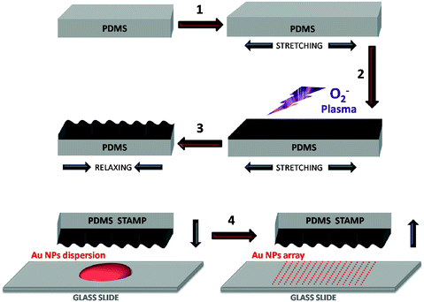 | ||
| Scheme 1 Preparation of the wrinkled PDMS stamp (1–3) and formation of gold nanoparticle arrays (4). Wrinkling process: A PDMS substrate is uniaxially stretched (1), and then treated with oxygen plasma to cross-link the top layer into a harder, thin SiOx film (2). The substrate is then relaxed to its original size forming wrinkles on the surface due to the hardness of the silica layer (3). Confining: A gold nanoparticle solution, drop-cast onto a glass slide, is confined with a wrinkled PDMS stamp (4). After solvent evaporation, the stamp is removed yielding a parallel arrangement of gold nanoparticles ordered in linear arrays. | ||
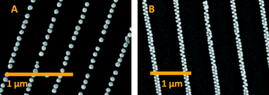 | ||
| Fig. 1 Scanning electron microscopy (SEM) images of two different stamped films, comprising single-line (A) and double-line (B) arrays of gold nanoparticles, upon confinement of a monodisperse gold colloid with wrinkled stamps of varying dimensions. Wrinkle wavelength and depth were determined by AFM to be 340 and 23 nm in A; 500 and 77 nm in B. | ||
Fig. 2 displays a summary of the optical characterization and theoretical modelling for both (single- and double-line) nanoparticle arrays. As expected, the optical properties (determined as scattering intensity from uniform regions using a dark field microspectroscopy setup as described in the ESI†) are affected by the details of the arrangement within each assembly. In both samples, the LSPR was found to be red-shifted with respect to the dilute gold colloid, as a consequence of plasmon coupling due to interactions between the electromagnetic fields of neighbouring particles.42 Interestingly, there are no significant differences between them, with maxima at 593 and 601 nm for the single-line and double-line arrays, respectively, though the double-line array yields a wider scattering band. Aggregation is well known to promote the formation of hot spots where high electromagnetic fields arise.2,43,44 For the specific arrangements obtained in this work, it is relatively simple to calculate the respective far field extinction spectra and the corresponding plasmonic near field enhancement at the maximum LSPR scattering wavelength, through modelling by means of the finite-difference time-domain (FDTD) method. For the calculation, two models were constructed in agreement with the experimental dimensions determined by SEM. The single-line array was simulated by a linear array of six nanoparticles (66 nm diameter), with an interparticle gap distance of 8 nm (Fig. 2C). The model for the double-line array comprised eight nanoparticles linearly aligned in two alternate rows, with a closest gap distance of 8 nm (Fig. 2D). Both model systems are fully consistent with SEM micrographs and the theoretical LSPR bands are in extremely good agreement with the experimental values (Fig. 2A,B), which strongly supports the validity of the models. Near field enhancement profiles, plotted at their corresponding LSPR maximum wavelengths, reveal that the electromagnetic field within the particle arrays is unevenly distributed, with significant enhancements precisely located at the gaps between nanoparticles, generating strong hot spots, in full agreement with the electromagnetic model in SERS.45
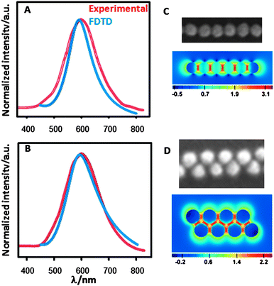 | ||
| Fig. 2 (A,B) Normalized experimental and calculated localized surface plasmon resonance bands for single-line (A) and double-line (B) stamped films. (C,D) Electric field intensity enhancement contours at a logarithmic scale for a single-line (C) Au nanoparticle array (excitation polarization along the x axis; mesh size 1 nm) and double-line (D) Au nanoparticle array (the profile was averaged over excitation polarizations at 0, 90, −58, and 58 degrees referred to the x axis; mesh size is 1.5 nm; contours are plotted in the xy plane). | ||
On the basis of the registered LSPR bands for the nanostructured substrates, the optical enhancing properties were tested using a laser excitation wavelength of 633 nm, upon exposure of the substrates to benzenethiol (BT) in gas phase. As a control, the same experiment was carried out on a physically evaporated gold island film, which is a conventional SERS substrate. It is important to point out that both dark field optical characterization and SERS mapping were carried out on the same specific areas of each substrate. Fig. 3A,B shows the white light, dark field and SERS images (normalized intensity at 1072 cm−1; Fig. 3C) obtained for the single- and double-line arrays. The first observation is that the SERS spectrum of BT, characterized by the CH bending (1022 cm−1) and the ring breathings (999 and 1072 cm−1), could be readily acquired from all points in the image. Further, in both cases the intensity of the SERS signal was highly uniform, in strong contrast to that obtained for the gold island film (Figure S5†). On the other hand, considering the average intensity (Fig. 3D), the island film was still found to outperform the nanoparticle arrays (almost double intensity). However, it should be taken into account that the sample preparation for SERS measurements (i.e. gas adsorption of a thiolated analyte) ensures that the probe creates a perfect Langmuir monolayer on the whole accessible gold surface. Thus, samples with a larger gold content will retain more analyte, with the subsequent increase in the SERS signal. Due to the ordered nature of the linear arrays and the high homogeneity in size and shape of the colloidal sample, it is possible to estimate the number of particles per sampled area. On the basis of the numerical aperture of the objective (0.9), the beam waist of the 100× objective is 430 nm with a 633 nm excitation laser line. Under such conditions and considering that the distance between grooves is 340 and 500 nm for single-line and double-line arrays as experimentally measured with SEM, a maximum of 1 line is probed in each scan. Moreover, the number of particles per sampled area (430 × 430 nm2) was experimentally counted to be around 6 and 12 for each sample, which is consistent with that theoretically expected (5.8 particles) by assuming a total particle diameter of 74 nm (particle + gap). Unfortunately, this method cannot be applied to the irregular gold film, but for a semiquantitative comparison we can consider that an area of 430 × 430 nm would contain 46 particles of the same size in cubic packing or 50 in hexagonal packing. With those numbers in mind we can carry out a correction of the overall intensity into “intensity per particle”, with the following results: 155, 99 and 41 counts for single-line, double-line and island film, respectively. As a consequence, the normalized enhancement by the single-line and double-line arrays is respectively three-fold and two-fold larger than that for an ideal island film. Additionally, this result suggests that the interaction resulting from order within a line is considerably more efficient than that created by the same particles ordered in a plane, in very good agreement with the electric field enhancement values estimated from FDTD. Fig. 2 C and D show that, whereas in both conformations hot spots are created at the gaps between particles, the electromagnetic field generated by the single-line array is up to one order of magnitude larger than that created by the double-line array. This concept becomes particularly important in ultrasensitive analysis since by simply decreasing the amount of nanostructured optical enhancer the detection limit will be increased because the formation of a monolayer will require a lower amount of analyte.46 Finally, an additional demonstration of the homogenous intensity provided by the substrate was obtained by sampling a large area of the single-line array. The results (Fig. 3E) clearly demonstrate that with this assembly method it is possible to control the organization of the colloidal particles on the substrate, with a consequent control over the formation of hot spots and the resulting SERS intensity, thus paving the road for the large scale development of highly-sensitive quantitative platforms, which have remained elusive so far.
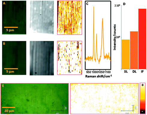 | ||
Fig. 3 (A,B) Optical, dark field and SERS images (λex: 633 nm; normalized intensity at 1072 cm−1; 8.5 × 12.5 μm2, step size 200 and 500 nm for x and y, respectively, with a total of 1062 spectra) for single-line (A) and double-line (B) nanoparticle arrays. (C) Representative SERS spectrum of benzenethiol. (D) Comparison of intensities between single-line (SL) and double-line (DL) nanoparticle arrays and a physically evaporated (IF) 9 nm gold island film; see electronic supplementary information for details.† (E) SERS mapping over a large area of particles arranged in single lines (λex: 633 nm; normalized intensity at 1072 cm−1; 105 × 45 μm2, step size 200 and 500 nm for x and y, respectively, with a total of 47![[thin space (1/6-em)]](https://www.rsc.org/images/entities/char_2009.gif) 250 spectra). Scale bar is the same for all the SERS maps. 250 spectra). Scale bar is the same for all the SERS maps. | ||
Homogeneously wrinkled stamps can be used to produce linear arrays of gold nanoparticles over large areas by confined drying of nanoparticle solutions. Depending on the dimensions of the grooves, the nanoparticles can be arranged into either single-line or double-line arrays, giving rise to marginally different optical response through plasmon coupling. Characterization of the SERS efficiency demonstrates high and extremely uniform enhancements for both types of assemblies, with higher values for the single-line arrays. This technique may become the method of choice for carrying out quantitative analysis while maintaining low detection limits.
Cristina Fernández-López is acknowledged for synthesizing the gold colloids. R.A.A.-P. acknowledges the RyC program (MEC, Spain). This work has been funded by the Spanish Ministerio de Ciencia e Innovación (Grants MAT2007-62696 and MAT2008-05755), the Xunta de Galicia (PGIDIT06TMT31402PR and 08TMT008314PR), and from the EU (NANODIRECT, grant number CP-FP 213948-2). A.F. and A.S. acknowledge funding from the German science foundation within the collaborative research project SFB 481, TP A14 and A.F. acknowledges funding from the German science foundation within the collaborative research project SFB 840, TP B5.
Notes and references
- N. P. Pieczonka and R. F. Aroca, Chem. Soc. Rev., 2008, 37, 946–954 RSC.
- L. Brus, Acc. Chem. Res., 2008, 41, 1742–1749 CrossRef CAS.
- L. Rodríguez-Lorenzo, R. A. Alvarez-Puebla, I. Pastoriza-Santos, S. Mazzucco, O. Stephan, M. Kociak, L. M. Liz-Marzán and F. J. García de Abajo, J. Am. Chem. Soc., 2009, 131, 4616–4618 CrossRef CAS.
- J. Kneipp, H. Kneipp and K. Kneipp, Chem. Soc. Rev., 2008, 37, 1052–1060 RSC.
- X. M. Qian and S. M. Nie, Chem. Soc. Rev., 2008, 37, 912–920 RSC.
- N. P. Pieczonka and R. F. Aroca, ChemPhysChem, 2005, 6, 2473–2484 CrossRef CAS.
- R. A. Alvarez-Puebla and L. M. Liz-Marzán, Small, 2010, 6, 604–610 CrossRef CAS.
- M. J. Banholzer, J. E. Millstone, L. Qin and C. A. Mirkin, Chem. Soc. Rev., 2008, 37, 885–897 RSC.
- R. A. Tripp, R. A. Dluhy and Y. Zhao, Nano Today, 2008, 3, 31–37 CrossRef CAS.
- S. Abalde-Cela, S. Ho, B. Rodriguez-Gonzalez, M. A. Correa-Duarte, R. A. Alvarez-Puebla, L. M. Liz-Marzan and N. A. Kotov, Angew. Chem., Int. Ed., 2009, 48, 5326–5329 CrossRef CAS.
- V. L. Schlegel and T. M. Cotton, Anal. Chem., 1991, 63, 241–247 CrossRef CAS.
- H. Ko, S. Singamaneni and V. V. Tsukruk, Small, 2008, 4, 1576–1599 CrossRef CAS.
- R. A. Alvarez-Puebla, R. Contreras-Cáceres, I. Pastoriza-Santos, J. Pérez-Juste and L. M. Liz-Marzán, Angew. Chem., Int. Ed., 2009, 48, 138–143 CrossRef CAS.
- R. M. Jarvis, H. E. Johnson, E. Olembe, A. Panneerselvam, M. A. Malik, M. Afzaal, P. O'Brien and R. Goodacre, Analyst, 2008, 133, 1449–1452 RSC.
- S. E. Bell and N. M. Sirimuthu, Chem. Soc. Rev., 2008, 37, 1012–1024 RSC.
- M. A. De Jesús, K. S. Giesfeldt, J. M. Oran, N. A. Abu-Hatab, N. V. Lavrik and M. J. Sepaniak, Appl. Spectrosc., 2005, 59, 1501–1508 CrossRef CAS.
- M. Abdelsalam, P. N. Bartlett, A. E. Russell, J. J. Baumberg, E. J. Calvo, N. G. Tognalli and A. Fainstein, Langmuir, 2008, 24, 7018–7023 CrossRef CAS.
- A. G. Brolo, E. Arctander, R. Gordon, B. Leathem and K. L. Kavanagh, Nano Lett., 2004, 4, 2015–2018 CrossRef CAS.
- J. P. Camden, J. A. Dieringer, J. Zhao and R. P. Van Duyne, Acc. Chem. Res., 2008, 41, 1653–1661 CrossRef CAS.
- Y. Fang, N. H. Seong and D. D. Dlott, Science, 2008, 321, 388–392 CrossRef CAS.
- K. E. Shafer-Peltier, C. L. Haynes, M. R. Glucksberg and R. P. Van Duyne, J. Am. Chem. Soc., 2003, 125, 588–593 CrossRef CAS.
- K. B. Biggs, J. P. Camden, J. N. Anker and R. P. Van Duyne, J. Phys. Chem. A, 2009, 113, 4581–4586 CrossRef CAS.
- S. Mahajan, J. J. Baumberg, A. E. Russell and P. N. Bartlett, Phys. Chem. Chem. Phys., 2007, 9, 6016–6020 RSC.
- A. Sánchez-Iglesias, P. Aldeanueva-Potel, W. Ni, J. Pérez-Juste, I. Pastoriza-Santos, R. A. Alvarez-Puebla, B. N. Mbenkum and L. M. Liz-Marzán, Nano Today, 2010, 5, 21–27 CrossRef CAS.
- C. Lu, H. Möhwald and A. Fery, Soft Matter, 2007, 3, 1530–1536 RSC.
- A. Horn, H. G. Schoberth, S. Hiltl, A. Chiche, Q. Wang, A. Schweikart, A. Fery and A. Böker, Faraday Discuss., 2009, 143, 143–150 RSC.
- A. Schweikart, A. Fortini, A. Wittemann, M. Schmidt and A. Fery, Manuscript submitted.
- J. Genzer and J. Groenewold, Soft Matter, 2006, 2, 310–323 RSC.
- A. Schweikart and A. Fery, Microchim. Acta, 2009, 165, 249–263 CrossRef CAS.
- J. Genzer and K. Efimenko, Science, 2000, 290, 2130–2133 CrossRef CAS.
- D. B. H. Chua, H. T. Ng and S. F. Y. Li, Appl. Phys. Lett., 2000, 76, 721–723 CrossRef CAS.
- L. M. Liz-Marzán, Langmuir, 2006, 22, 32–41 CrossRef CAS.
- M. Grzelczak, J. Perez-Juste, P. Mulvaney and L. M. Liz-Marzan, Chem. Soc. Rev., 2008, 37, 1783–1791 RSC.
- I. Pastoriza-Santos and L. M. Liz-Marzán, Adv. Funct. Mater., 2009, 19, 679–688 CrossRef.
- C. J. Murphy, T. K. Sau, A. M. Gole, C. J. Orendorff, J. Gao, L. Gou, S. E. Hunyadi and T. Li, J. Phys. Chem. B, 2005, 109, 13857–13870 CrossRef CAS.
- P. N. Njoki, I.-I. S. Lim, D. Mott, H.-Y. Park, B. Khan, S. Mishra, R. Sujakumar, J. Luo and C.-J. Zhong, J. Phys. Chem. C, 2007, 111, 14664–14669 CrossRef CAS.
- J. Rodríguez-Fernández, A. M. Funston, J. Pérez-Juste, R. A. Alvarez-Puebla, L. M. Liz-Marzán and P. Mulvaney, Phys. Chem. Chem. Phys., 2009, 11, 5909–5914 RSC.
- J. Nelayah, M. Kociak, O. Stéphan, F. J. García de Abajo, M. Tencé, L. Henrard, D. Taverna, I. Pastoriza-Santos, L. M. Liz-Marzán and C. Colliex, Nat. Phys., 2007, 3, 348–353 CrossRef CAS.
- G. W. Bryant, F. J. García de Abajo and J. Aizpurua, Nano Lett., 2008, 8, 631–636 CrossRef CAS.
- J. Rodríguez-Fernández, J. Pérez-Juste, F. J. García de Abajo and L. M. Liz-Marzán, Langmuir, 2006, 22, 7007–7010 CrossRef CAS.
- H. Wang, J. Kundu and N. J. Halas, Angew. Chem., Int. Ed., 2007, 46, 9040–9044 CrossRef CAS.
- T. Ung, L. M. Liz-Marzán and P. Mulvaney, J. Phys. Chem. B, 2001, 105, 3441–3452 CrossRef CAS.
- G. Braun, I. Pavel, A. R. Morrill, D. S. Seferos, G. C. Bazan, N. O. Reich and M. Moskovits, J. Am. Chem. Soc., 2007, 129, 7760–7761 CrossRef CAS.
- J. M. Baik, S. J. Lee and M. Moskovits, Nano Lett., 2009, 9, 672–676 CrossRef CAS.
- M. Moskovits, J. Raman Spectrosc., 2005, 36, 485–496 CrossRef CAS.
- M. Spuch-Calvar, L. Rodríguez-Lorenzo, M. P. Morales, R. A. Alvarez-Puebla and L. M. Liz-Marzán, J. Phys. Chem. C, 2009, 113, 3373–3377 CrossRef CAS.
Footnote |
| † Electronic supplementary information (ESI) available: Materials and methods; AFM analysis of wrinkled PDMS stamps; TEM images and localized surface plasmon resonances for the gold nanoparticles as prepared; other orientations for the electric field intensity enhancement contours; and, LSPR, SEM and optical and SERS images for a 9 nm gold island film. See DOI: 10.1039/c0sc00132e |
| This journal is © The Royal Society of Chemistry 2010 |