Unique three-dimensional (3D) molecular array in dimethyl-DNTT crystals: a new approach to 3D organic semiconductors†
Myeong Jin
Kang
,
Tatsuya
Yamamoto‡
,
Shoji
Shinamura
,
Eigo
Miyazaki
and
Kazuo
Takimiya
*
Department of Applied Chemistry, Graduate School of Engineering, Hiroshima University, Higashi-Hiroshima, 739-8527, Japan. E-mail: ktakimi@hiroshima-u.ac.jp; Fax: +81-82-424-5494
First published on 26th May 2010
Abstract
Two isomeric dimethyl derivatives of dinaphtho[2,3-b:2′,3′-f]thieno[3,2-b]thiophene (2,9- and 3,10-DMDNTT) were synthesized and characterized. Their crystal structures were classified as unique three-dimensional (3D) herringbone arrangements. Of them, 3,10-DMDNTT preserves the same packing structure in the thin-film phase, and the film acted as a superior semiconductor channel in field-effect transistors with mobility up to 0.8 cm2 V−1 S−1.
Control of dimensionality of the electronic structure in organic molecular solids is crucially important for the development of high performance organic electronic devices. For example, organic thin-film transistors (OTFTs), in which carrier transport takes place between the source and drain electrodes in the transverse direction, require a semiconducting channel with a two-dimensional (2D) electronic structure to realize high carrier mobility.1 In fact, organic semiconductors that form a crystalline, layered structure with 2D herringbone packing tend to give OTFTs with better performance, as well-exemplified by the pentacene-based OTFTs.2
On the other hand, molecular materials that enable three-dimensional (3D) electronic structures are very limited. C60, the spherical π-electron system that affords a 3D structure is rather exceptional,3 because most π-conjugated systems have planar molecular structures. For this reason, to construct 3D structure using planar π-systems has been a great challenge. To address this issue, several approaches have been taken,4 and recently Skabara and co-workers have reported that orthogonally oriented π-stacks of a benzo[1,2-d;4,5-d′]bisthiazole derivative (1, Fig. 1) interconnected by intermolecular contacts through non-bonded sulfur and nitrogen atoms affords a 3D interactive electronic structure of utility for OTFTs with a field-effect mobility (μFET) as high as 10−2 cm2 V−1 S−1.5
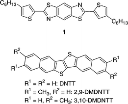 | ||
| Fig. 1 Molecular structure of 1 and DNTT derivatives. | ||
Recently, we reported the synthesis and characterization of dinaphtho[2,3-b:2′,3′-f]thieno[3,2-b]thiophene (DNTT, Fig. 1) together with its OTFTs showing μFET up to 3.1 cm2 V−1 s−1.6 Structural characterizations of its single crystal and thin film indicated that DNTT forms a typical 2D electronic structure with a herringbone arrangement. In order to investigate the effect of molecular modification of DNTT, we have synthesized two isomeric dimethyl derivatives (2,9-DMDNTT and 3,10-DMDNTT, Fig. 1) and found that these two compounds have intriguing 3D crystal structures in the solid state. In this edge article, we report the synthesis of two DMDNTTs, their single crystal structures, thin film structures, and OTFT properties, and discuss the influence of the 3D structure on the OTFT characteristics.
Syntheses of 2,9- and 3,10-DMDNTTs were successfully carried out using the same synthetic strategy as the parent DNTT (Scheme 1). 6- (3a) and 7-methyl-2-naphthaldehyde (3b) were selectively synthesized from 2,6- (2a) and 2,7-dimethylnaphthalene (2b), respectively, according to the reported procedure.7 Introduction of methylthio groups at the 3-positions followed by conversion of the aldehyde functionality of 4 to an olefin moiety with a low valent titanium reagent gave the precursors (5a and 5b) in reasonable yields. Finally, the ring closing reaction to construct the thieno[3,2-b]thiophene substructure6,8 afforded the desired DMDNTT derivatives. Electrochemical measurements using cyclic voltammetry (CV) showed that both DMDNTTs have slightly elevated HOMO energy levels than that of the parent DNTT (∼−5.4 eV below the vacuum level) by ca. 0.1 eV (Fig. S1†). Optical bandgaps of the DMDNTTs estimated from the absorption onsets in their UV-vis spectra (Fig. S2†) were ca. 2.9 eV, which are almost the same as that of the parent DNTT. From these physicochemical data, we concluded that the methyl groups introduced to the DNTT core act as weak electron donating groups, but the extent of the electron donating effect is rather limited, resulting in almost similar properties to those of the parent DNTT. In fact, two DMDNTTs are stable compounds to air, similar to the parent DNTT. In addition, there is no apparent difference between 2,9- and 3,10-DMDNTTs in their electronic properties.
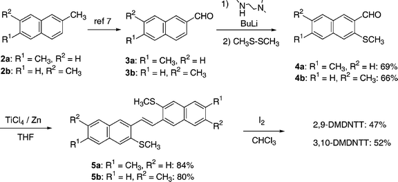 | ||
| Scheme 1 Syntheses of 2,9- and 3,10-DMDNTT. | ||
Fig. 2 shows the crystal structures of DMDNTTs elucidated by single-crystal X-ray analysis.9 From the molecular arrangements projected along the molecular long axis direction (Fig. 2a and c), it seems that both structures are classified as having typical herringbone packing. However, both compounds crystallize with slippage along the molecular long axis direction by about the half a molecular length. In the packing arrangement of 2,9-DMDNTT (Fig. 2a), the molecules in the b-axis direction are at the same depth and interact with each other in a face-to-edge manner, consisting of one-dimensional (1D) molecular ribbons. The neighboring molecular ribbons along the c-axis direction exist with slippage along the molecular long axis direction, resulting in relatively weak intermolecular interactions via the naphthalene moieties in the c-axis direction (Fig. 2b). Thus, the crystal structure, as a whole, is classified as a new type of 3D packing, which can be expressed as a “3D-herringbone” packing.
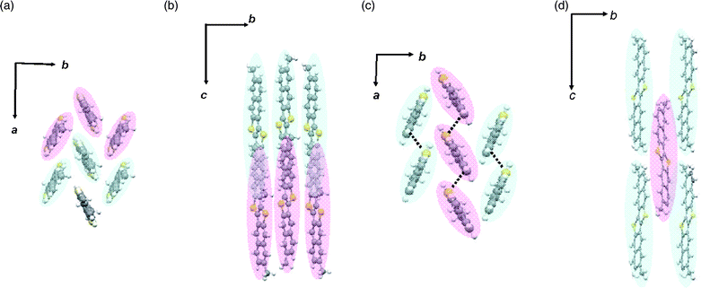 | ||
| Fig. 2 Molecular arrangements of 2,9- (a and b) and 3,10-DMDNTT (c and d). Projection view along the molecular long axis direction (a and c), and side view of the molecular arrangements (b and d). The molecules with the same color exist in the same depth in each projection. | ||
On the other hand, 3,10-DMDNTT has a different molecular arrangement from that of 2,9-DMDNTT: in the molecular arrangement of 3,10-DMDNTT (Fig. 2c), the molecules along the a-axis direction are at the same depth and interact with each other in an edge-to-edge manner, consisting of 1D molecular stacks with short intermolecular S–S contacts (3.52 Å, dotted lines in Fig. 2c). The neighboring stacks along the b-axis direction exist with slippage, resulting in a different type of 3D-herringbone packing. Occurrence of the slippage in both structures is probably due to the steric hindrance caused by the methyl groups in the case of ordinary herringbone packing with a layer-by-layer structure. Therefore, it can be concluded that introduction of methyl groups at the ends of the DNTT molecule can change the packing arrangement drastically in bulk single crystals. Provided that the same molecular arrangements are preserved in the thin film state, DMDNTTs will be interesting molecular materials possessing 3D structure and give a chance to investigate the effect of 3D structure in thin film devices. We thus prepared thin films of DMDNTTs on Si/SiO2 substrates by vapor deposition and then tested them as active channels of OTFTs.
In order to determine the structural phases, out-of-plane and in-plane X-ray diffractions (XRDs) of evaporated thin films were measured. Fig. 3 shows the XRD patterns of DMDNTTs together with the simulated powder patterns based on their bulk single crystal structures. Comparison of the XRD patterns with the powder pattern of 2,9-DMDNTT (Fig. 3a) obviously indicates that the thin film phase and the bulk crystal phase are different. From the out-of-plane XRD patterns, the interlayer spacing (d-spacing) is estimated to be ca. 20 Å, which is almost the same as the molecular length, indicating that 2,9-DMDNTT takes the layer-by-layer structure in the thin film phase similar to the parent DNTT and other ordinary organic semiconductors. The existence of polymorphism implies that the 3D bulk phase is metastable, and, upon deposition on the surface of the substrate, the ordinary layer-by-layer structure, i.e., a thin film phase, was predominantly formed.
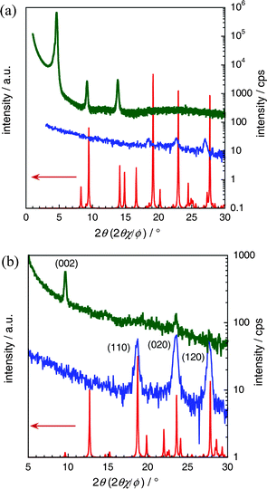 | ||
| Fig. 3 Out-of-plane (green) and in-plane (blue) XRD patterns together with the simulated powder pattern from the bulk single crystal phase (red) for 2,9- (a) and 3,10-DMDNTT (b). It should be noted that both in-plane and out-of-plane peaks are indexed by the powder pattern for 3,10-DMDNTT (b), whereas an apparent difference between the experimental thin-film XRDs and the simulated powder pattern for 2,9-DMDNTT (a) was observed. | ||
On the other hand, all the peaks observed in both the out-of-plane and in-plane XRDs of the 3,10-DMDNTT thin film are well-assigned by the simulated powder pattern of the bulk single crystal phase (Fig. 3b), indicating that the 3D herringbone structure is preserved in the thin film state. The preferable orientation of the crystallites in the thin film is also determined to be the crystallographic c-axis that stands along the substrate normal (Fig. 2d). As a result, two DMDNTTs have distinct molecular orderings in the thin film phase, although the molecular electronic structures are quite similar to each other. This means that DMDNTTs can be an ideal material class to clarify the effect of 3D structure in thin film transistors.
OTFT devices with a top contact configuration (L = 40–190 μm, W = 1500 μm) showed typical p-channel transistor behaviors for both compounds (Fig. 4), and extracted mobilities from the saturation regime are ∼0.4 cm2 V−1 S−1 for 2,9-DMDNTT and ∼0.8 cm2 V−1 S−1 for 3,10-DMDNTT, respectively. These mobilities are lower than that of the parent DNTT (∼3.0 cm2 V−1 S−1), which can be ascribed to the difference of the molecular packing in the thin film state. For the parent DNTT, well-ordered 2D structure with large intermolecular overlaps facilitates carrier transport. 2,9-DMDNTT will have a similar molecular arrangement in the thin film to that of DNTT, but owing to the methyl groups, close intermolecular overlap would be hindered, resulting in decreased carrier mobility.
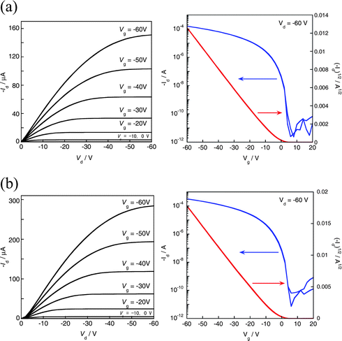 | ||
| Fig. 4 FET characteristics of (a) 2,9-DMDNTT- and (b) 3,10-DMDNTT-based devices (L = 90 μm, W = 1500 μm) fabricated on an octyltrichlorosilane (OTS)-treated substrate at Tsub = 60 °C. | ||
On the other hand, it is speculated that the 3D structure of 3,10-DMDNTT is not necessarily suitable for 2D (in-plane) carrier transport in the thin film transistor setting, because the molecular orbital overlaps along the crystallographic b-axis should be smaller than those in the a-axis direction, owing to the slippage of the molecules along the c-axis direction (Fig. 2d). However, the mobility value for 3,10-DMDNTT-based TFTs is unexpectedly high and comparable to other ordinary 2D herringbone systems including 2,9-DMDNTT. Furthermore, compared with the 1-based OTFTs (mobility ∼10−2 cm2 V−1 S−1) with 3D electronic structure,5 the present 3,10-DMDNTT-based TFTs are superior in terms of not only mobility but also Ion/off and subthreshold swing. To understand the high performance of the present 3,10-DMDNTT-based devices, we tried to evaluate its electronic structure quantitatively.
To this end, we employed the theoretical calculation of intermolecular transfer integrals (t) of HOMOs using the Amsterdam Density Functional (ADF) program package.10,11 As depicted in Fig. 5a, the transfer integrals in the stacks (i.e., along the crystallographic a-axis direction) designated as ta are 67 meV, which is almost the same as the transfer integrals in the parent DNTT stacks (71 meV).12 On the other hand, the transfer integrals in the transverse direction (tp) are calculated to be 9 meV (Fig. 5a, b). Although the tp value is smaller than ta (ca. one seventh), substantial intermolecular overlaps of HOMOs are confirmed in the crystallographic bc plane, indicating that the electronic structure of 3,10-DMDNTT can be regarded as an anisotropic quasi 3D system. Despite the large slippage along the molecular long axis direction, relatively effective intermolecular orbital overlaps remain. This is probably because half of the DNTT core is large enough to keep effective intermolecular orbital overlaps.
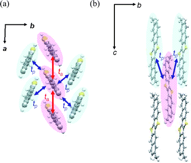 | ||
| Fig. 5 Calculated intermolecular transfer integrals (t) between HOMOs in 3,10-DMDNTT crystals. ta (along the a-axis direction): 67 meV, tp (in the bc plane): 9 meV. | ||
In summary, we have successfully synthesized two isomeric DMDNTT derivatives selectively. The electronic properties of two DMDNTTs are basically the same as each other: similar HOMO energy levels and HOMO–LUMO gaps. In addition, they have similar 3D crystal structures (3D herringbone packing) in the bulk single crystal. However, only 3,10-DMDNTT preserves the same 3D structure in the thin film state, whereas 2,9-DMDNTT takes an ordinary layered structure in the thin film. Although such 3D herringbone packing in the thin film state was thought to be unsuitable for high performance OTFT devices, 3,10-DMDNTT showed quite high mobility (∼0.8 cm2 V−1 S−1). Theoretical evaluation of electronic structure in the thin film state indicated that 3,10-DMDNTT has an anisotropic 3D electronic structure with very large intermolecular overlaps in the a-axis direction (67 meV) and relatively large overlaps (9 meV) in the bc plane. Since the device configuration of the thin film transistor is not necessarily suitable to take advantage of the 3D electronic structure, the present kind of 3D structure will have potential as an active layer in other types of organic devices, in particular so called “vertical devices” such as organic static induction transistors (OSITs),13 organic light emitting diodes (OLEDs),14 or organic photovoltaics (OPVs).15
For the development of 3D electronic structure materials based on planar π-systems, the present results will give insight into the molecular design strategy: introduction of methyl groups to linearly extended planar π-systems will be a potential approach. Further investigation in this direction as well as application of the 3,10-DMDNTT thin film to other thin film devices are now underway in our group.
Acknowledgements
This work was partially supported by Grants-in-Aid for Scientific Research from the Ministry of Education, Culture, Sports, Science and Technology, Japan (No. 20350088) and NEDO Nanotech Challenge Program. We thank Rigaku Corp. for in-plane XRD measurements.Notes and references
- (a) C. D. Dimitrakopoulos and P. R. L. Malenfant, Adv. Mater., 2002, 14, 99 CrossRef CAS; (b) J. A. Rogers, Z. Bao, H. E. Katz and A. Dodabalapur, in Thin-Film Transistors, ed. C. R. Kagan and P. Andry, Marcel Dekker, New York 2003, p. 377 Search PubMed; (c) J.-L. Bredas, D. Beljonne, V. Coropceanu and J. Cornil, Chem. Rev., 2004, 104, 4971 CrossRef CAS; (d) V. Coropceanu, J. Cornil, D. A. da Silva Filho, Y. Olivier, R. Silbey and J.-L. Bredas, Chem. Rev., 2007, 107, 926 CrossRef CAS.
- (a) D. J. Gundlach, Y. Y. Lin, T. N. Jackson, S. F. Nelson and D. G. Schlom, IEEE Electron Device Lett., 1997, 18, 87 CrossRef CAS; (b) T. W. Kelley, L. D. Boardman, T. D. Dunbar, D. V. Muyres, M. J. Pellerite and T. P. Smith, J. Phys. Chem. B, 2003, 107, 5877 CrossRef CAS; (c) H. Klauk, M. Halik, U. Zschieschang, F. Eder, G. Schmid and C. Dehm, Appl. Phys. Lett., 2003, 82, 4175 CrossRef CAS.
- R. C. Haddon, Acc. Chem. Res., 1992, 25, 127 CrossRef CAS.
- J. Roncali, P. Leriche and A. Cravino, Adv. Mater., 2007, 19, 2045 CrossRef CAS.
- H. Pang, F. Vilela, P. J. Skabara, J. J. W. McDouall, D. J. Crouch, T. D. Anthopoulos, D. D. C. Bradley, D. M. de Leeuw, P. N. Horton and M. B. Hursthouse, Adv. Mater., 2007, 19, 4438 CrossRef CAS.
- (a) T. Yamamoto and K. Takimiya, J. Am. Chem. Soc., 2007, 129, 2224 CrossRef CAS; (b) T. Yamamoto and K. Takimiya, J. Photopolym. Sci. Technol., 2007, 20, 57 CrossRef CAS.
- K. A. Muszkat, A. Jakob, N. Castel, E. Fisher, K. Rauch and W. Lüttke, J. Photochem. Photobiol., A, 1991, 60, 193 CrossRef CAS.
- T. Izawa, E. Miyazaki and K. Takimiya, Chem. Mater., 2009, 21, 903 CrossRef CAS.
- Crystallographic data for DMDNTTs. 2,9-DMDNTT: C24H16S2, M = 368.49, monoclinic, space group P21 (#4), a = 11.686(12), b = 7.737(7), c = 10.674(11) Å, β = 114.187(5)°, V = 880.4(15) Å3, T = 293 K, Z = 2, reflections measured 7063, 3857 unique which were used in all calculations. The final R1 was 0.0731 (>2σ(I)), and the final wR on F2 was 0.1929 (all data). CCDC 763568. 3,10-DMDNTT: C24H16S2, M = 368.49, monoclinic, space group P21/n (#14), a = 6.148(2), b = 7.535(3), c = 18.559(7) Å, β = 97.9240(10)°, V = 851.5(5) Å3, T = 293 K, Z = 2, reflections measured 6211, 1839 unique which were used in all calculations. The final R1 was 0.0396 (>2σ(I)), and the final wR on F2 was 0.1146 (all data). CCDC 763569.
- (a) ADF2008.01, SCM, Theoretical Chemistry, Vrije Universiteit, Amsterdam, The Netherlands, http://www.scm.com Search PubMed; (b) P. Prins, K. Senthilkumar, F. C. Grozema, P. Jonkheijm, A. P. H. J. Schenning, E. W. Meijer and L. D. A. Siebbeles, J. Phys. Chem. B, 2005, 109, 18267 CrossRef CAS.
- (a) M.-Y. Kuo, H.-Y. Chen and I. Chao, Chem.–Eur. J., 2007, 13, 4750 CrossRef CAS; (b) Y.-C. Chang, Y.-D. Chen, C.-H. Chen, Y.-S. Wen, J. T. Lin, H.-Y. Chen, M.-Y. Kuo and I. Chao, J. Org. Chem., 2008, 73, 4608 CrossRef CAS.
- T. Yamamoto, S. Shinamura, E. Miyazaki and K. Takimiya, Bull. Chem. Soc. Jpn., 2010, 83, 120 CrossRef CAS.
- (a) D. X. Wang, Y. Tanaka, M. Iizuka, S. Kuniyoshi, K. Kudo and K. Tanaka, Jpn. J. Appl. Phys., 1999, 38, 256 CrossRef CAS; (b) K. Kudo, D. X. Wang, M. Iizuka, S. Kuniyoshi and K. Tanaka, Synth. Met., 2000, 111–112, 11 CrossRef CAS.
- C. W. Tang and S. A. VanSlyke, Appl. Phys. Lett., 1987, 51, 913 CrossRef CAS.
- (a) C. W. Tang, Appl. Phys. Lett., 1986, 48, 183 CrossRef CAS; (b) J. G. Xue, S. Uchida, B. P. Rand and S. R. Forrest, Appl. Phys. Lett., 2004, 85, 5757 CrossRef CAS; (c) K. Suemori, T. Miyata, M. Yokoyama and M. Hiramoto, Appl. Phys. Lett., 2005, 86, 063509 CrossRef; (d) K. L. Mutolo, E. I. Mayo, B. P. Rand, S. R. Forrest and M. E. Thompson, J. Am. Chem. Soc., 2006, 128, 8108 CrossRef CAS; (e) K. Sakai and M. Hiramoto, Mol. Cryst. Liq. Cryst., 2008, 491, 284 CrossRef CAS.
Footnotes |
| † Electronic supplementary information (ESI) available: Experimental details of the synthesis and physicochemical characterization of DMDNTTs and device fabrication and evaluation. CCDC reference numbers 763568 and 763569. For ESI and crystallographic data in CIF or other electronic format see DOI: 10.1039/c0sc00156b |
| ‡ Present address: Research Centre for Composite Device Technology, Iwate University, Hanamaki, Iwate 025-0312, Japan. E-mail: tyama@iwate-u.ac.jp; Fax: +81-198-30-1170; Tel: +81-198-30-1170 |
| This journal is © The Royal Society of Chemistry 2010 |