Mechanically-controllable single molecule switch based on configuration specific electrical conductivity of metal–molecule–metal junctions†
Masateru
Taniguchi
*ab,
Makusu
Tsutsui
a,
Kazumichi
Yokota
a and
Tomoji
Kawai
*a
aThe Institute of Scientific and Industrial Research, Osaka University, Ibaraki, Osaka 567-0047, Japan. E-mail: taniguti@sanken.osaka-u.ac.jp; kawai@sanken.osaka-u.ac.jp; Fax: +81-6-6875-2440; Tel: +81-6-6879-8446
bPRESTO, Japan Science and Technology Agency, Honcho, Kawaguchi, Saitama 332-0012, Japan. Fax: +81-48-226-5651; Tel: +81-48-226-5601
First published on 27th May 2010
Abstract
We report the systematic characterization of configuration-specific electrical conductivity in metal–molecule–metal structures for a demonstration of mechanically controllable contact effect single-molecule switches. Break junction measurements reveal two distinct conductance states of GH ∼ 1.3 mG0 and GL ∼ 0.4 mG0 in an Au–hexanedithiol–Au system. We provide evidence that transitions from GH to GL involve atom scale deformations between two distinct metal–molecule contact configurations by conducting single molecule inelastic electron tunneling spectroscopy. We also examine mechanically controlled binary switching via bistable conductance states, thereby attaining an alkanedithiol single-molecule switch.
Introduction
Advances in technology for building metal–molecule–metal systems have provided new opportunities for exploring single molecule electron transport and concomitant impressive progress in demonstrating unique functions of individual organic molecules toward molecular electronics.1–8 One of the fascinating molecular device concepts is to exploit geometry specific electrical conductivity;9,10 it has been established that conductance of single molecule junctions varies extensively with atomic scale changes in molecular conformations and metal–molecule contact configurations.11–13 This has led to an idea of the smallest single-molecule switch leveraging the geometrical sensitivity,9 the key concept of which lies in conductance switching via dynamic structural controls of metal–molecule–metal bridges between two characteristic configurations by mechanical means.Geometrical dependence of single molecule electron transport has been the subject of extensive study.14–18 Particularly, Au–alkanedithiol–Au junctions have been widely employed as a benchmark system: several groups have consistently observed more than one distinctive single molecule conductance state, which are interpreted a priori as reflecting the difference in electrode–molecule coupling associated with variations in Au–thiol motif, i.e. top–top, top–hollow, and hollow–hollow arrangements.14–18 We report herein the demonstration of a mechanically controllable contact effect single molecule switch that exploits the characteristic configuration derived multiple conductance states in Au–1,6-hexanedithiol (HDT)–Au bridges.
Experimental
Stable molecular junctions were formed using nanofabricated mechanically-controllable break junctions (nano-MCBJs).19,20 Fabrication procedures of nano-MCBJs are described elsewhere.19 Briefly, Au nanoscale junctions were patterned on a polyimide-coated flexible metal substrate using a standard electron beam lithography technique and subsequent lift-off. The samples were then exposed to isotropic reactive ion etching. As a result, we obtained free-standing Au junctions (narrowest cross section is approximately 100 nm × 100 nm). Sample substrates were subjected to three-point bending using a piezo-actuator-driven pushing rod in order to break the junctions and form a pair of nanoelectrodes. Au nanobridges were designed to provide the damping factor of Δd/ΔL ∼ 3 × 10−4,19 where Δd and ΔL are the displacements of the nanoelectrodes and the moving distance of the pushing rod, respectively. This low displacement ratio allowed fine control of the electrode gap distance at sub-picometre resolution and also offered sufficiently high mechanical stability for forming and holding metal–molecule–metal structures for prolonged times.20,21Single molecule conductance measurements were performed as follows. To begin with, Au junctions were broken by bending the substrate of a nano-MCBJ sample in a dilute HDT solution of 1,2,4-trichlorobenzene (0.01 mM), which allowed molecular adsorptions on the fresh fracture surface. Subsequently, we evacuated a chamber to remove the solvent. When reaching a vacuum level of <10−5 Torr, we exhibited break junction experiments at room temperatures under a constant dc bias Vb of 0.2 V exploiting a resistance feedback program with a stretching speed vd of 6 pm s−1 and concurrently monitored junction conductance G utilizing a digital oscilloscope (Waverunner 6051A, Lecroy) and a picoammeter (Keithley 6487).20,21 This automated procedure optimizes strain relief via thermally-induced contact atom rearrangements during mechanical elongations and realizes stable single molecule bridging.22
Inelastic electron tunneling spectroscopy measurements were performed by first forming a stable single molecule junction using the self-breaking technique.22 Subsequently, we held the junction and performed a lock-in measurement (SR830, Stanford Research Systems) with a modulation voltage of 10 mV at 1 kHz in a bias range of −0.4 V ≤ Vb ≤ 0.4 V. Output current was amplified by a preamplifier (Keithley 428) and the first harmonic was recorded using a 24-bit signal acquisition module (NI USB-9234). Vibrational spectra were then obtained numerically from the acquired dI/dVb–Vb curves.
Results and discussion
Measurements of HDT single molecule junction conductance
G–t traces during junction elongation processes display a plateau feature at around 1 G0 (G0 = 2e2/h is a conductance quantum where e and h are the electron charge and Planck's constant respectively) (Fig. 1). This distinguishing characteristic signifies the formation of Au single atom contacts that possess one fully-opened channel for electron transmission.23,24 Further stretching leads to sudden drops in G by eventual fracture of Au contacts. At this breakdown stage, about 60% of 1500 G–t curves acquired show a rapid conductance decrease to zero. On the other hand, we occasionally observe (about 30%) another conductance plateau at around 10−3G0 (Fig. 1). The low-G steps are naturally regarded as denoting bridging of one or a few molecules between nano-MCBJ electrodes.2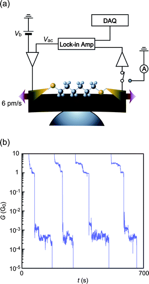 | ||
| Fig. 1 (a) Schematic illustrations of the experimental setup exploited for single molecule conductance and IETS measurements of Au–hexanedithiol–Au systems using nano-MCBJs. (b) Typical G–t curves obtained during junction breaking under a stretching rate of 6 pm s−1 at room temperature. Clear conductance steps at around 1 mG0 signify the formation of stable Au–HDT–Au bridges. | ||
A conductance histogram constructed with G–t curves wherein low-G steps (504 curves) are detected exhibits a multi-peak profile as shown in Fig. 2 (details about the data selection procedure are summarized in the ESI Fig. S1 and S2†). Two peaks are located at 1.3 × n mG0 whereas another two can be found at 0.4 × n mG0 (n = 1, 2). The regularly positioned peaks correspond to conductance states of metal–molecule–metal junctions with n number of molecules connected in parallel.2 This manifests an existence of two distinct conductance states at GH ∼ 1.3 mG0 and GL ∼ 0.4 mG0 for Au–HDT–Au single molecule junctions. It is of note that GH and GL are in good accordance with previous reports.14,16,25 The multiple conductance states have been attributed to conformational distortions in alkyl chains and hollow-to-top structural transitions at Au–thiol contacts by arguing possible atomistic deformations of metal–molecule–metal systems occurring in the course of break junction experiments.14,16
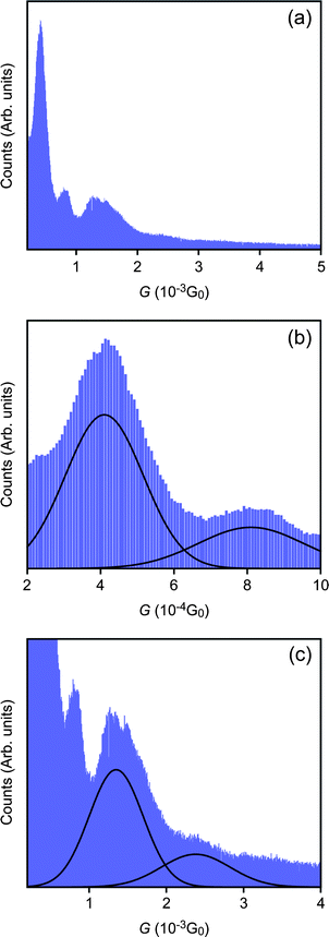 | ||
| Fig. 2 Conductance histograms built with G–t traces that demonstrated clear low-G steps below 1 G0 (504 curves out of 1500 traces measured). (a) The histogram shows a multi-peak structure. (b) Regularly positioned peaks at integer multiples of about 1.3 mG0 and (c) 0.4 mG0. The solid lines are Gaussian fits to the peak profiles. This confirms an existence of two distinct conductance states at GH ∼ 1.3 mG0 and GL ∼ 0.4 mG0 in Au–HDT–Au single molecule junctions. | ||
Mechanically-controlled conductance switching of HDT single molecule junctions
Having characterized the single molecule conductance, we demonstrate mechanically controlled conductance switching in single HDT molecules. Forming a single molecule junction by the self-breaking technique at room temperature, we imposed a repeated mechanical elongation/compression immediately following observation of a conductance jump from GH to GL by implementing a sinusoidal motion of the piezo-actuator. The resultant junction displacements Δd amounted to ∼0.3 nm at a modulation frequency νp. Consequently, the molecular junction exhibited conductance switching between GH and GL in a regular fashion complying with the introduced mechanical oscillations at νp = 1 Hz (Fig. 3(a)) and at νp = 0.1 kHz (Fig. 3(b, c)). We emphasize that the G–t characteristics are represented as a telegraphic waveform. The discrete change of G in response to the smooth sine-wave perturbations certifies that the conductance switching indeed occurs via transitions between two particular metal–molecule–metal configurations. The present results serve to validate the utility of geometry-specific conductance of metal–molecule–metal systems in single molecule switch applications.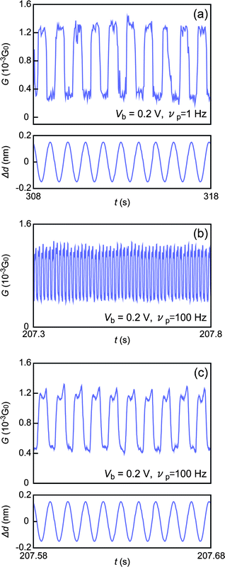 | ||
| Fig. 3 Contact effect switching in HDT single molecule junctions between GH and GL implemented by imposing sinusoidal mechanical oscillations of frequency νp to activate repeated structural transitions at the Au–S contacts. (a) Switching characteristics obtained under applied mechanical perturbations with peak-to-peak displacements of approximately 0.3 nm at νp = 1 Hz and (b, c) νp = 0.1 kHz. Lower panels in (a) and (c) depict the displacements of nano-MCBJ electrodes introduced. | ||
It should be noted that stable single molecule switching characteristics may not be obtained reproducibly unless suitable experimental conditions are adopted. A mechanical transition of HDT single molecule junctions from GH to GL occurs when a certain level of strain is exerted externally to change the Au–S contact configurations from hollow to top geometries, and vice versa. The amount of strain necessary to switch Au–S contact configurations at a given temperature and bias voltage is dependent on the actual strain rate, and hence 2Δdνp, due to the nature of single molecule junctions undergoing thermoactivated breakdown at room temperatures.20,21,26,27 At 1 Hz ≤ νp ≤ 100 Hz, we observed stable configurational switching between GH and GL at Δd ∼ 0.3 nm. When Δd > 0.4 nm, the molecular junctions became increasingly unstable especially at low νp conditions where external displacements would become larger than the junction breakdown length of single molecule junctions suspended via Au–S contacts. On the other hand, conductance switching was seldom observed in cases when Δd < 0.2 nm because of inadequate strain.
Vibrational characteristics of HDT single molecule junctions
Aiming to unravel the switching mechanism, we next sought to identify the relevant molecular junction configurations for GH and GL states. This should entail direct experimental examinations of the underlying atom-scale configuration deformations. Combining the techniques of the mechanically-controllable break junction method and inelastic electron tunneling spectroscopy (MCBJ-IETS) is a powerful analytical tool that allows single molecule identifications in metal–molecule–metal structures.28–30 Moreover, it has been predicted theoretically that IETS can potentially serve as a direct probe for atom-scale geometries of molecular junctions.31–34 Here we characterized the configuration-specific conductivity in metal–molecule–metal systems using the MCBJ-IETS technique.29,30 HDT single molecule junctions were formed at 4.2 K by the self-breaking method20 under Vb = 0.2 V and vd = 6 pm s−1 (we presume that the single molecule conductance of Au–HDT–Au junctions is independent of temperature considering the relatively wide HOMO–LUMO energy gap). A plateau was observed at around GH by monitoring the time evolution of G during a molecular junction formation (Fig. 4(a)). Subsequently, we measured the differential conductance in a bias range of −0.4 V ≤ Vb ≤ 0.4 V using a standard lock-in method. The thus acquired dI/dVb–Vb curve demonstrates a stepwise increase with Vb (Fig. 4(b)). The dI/dVb steps signify contributions of inelastic electron tunneling through excitations of IETS-active molecular vibrations by tunneling electrons. d2I/dVb2–Vb curves are derived numerically from the dI/dVb data (Fig. 4(c)). The obtained IET spectra show several peaks at Vb = Vp where dI/dVb steps emerge and hence inelastic tunneling channels open. Therefore, Vp is related to an IETS-active molecular vibration mode energy hν as eVp = hν. Table 1 lists Vp extracted from positions of the peaks labeled by numbers. We assessed possible candidates for relevant IETS-active molecule vibration modes that can be assigned to Vp by theoretically deducing the vibrational frequencies using the GAUSSIAN03 program.35 The calculations were conducted on a single HDT molecule connected to two gold clusters composed of 13 gold atoms using density functional theory with the B3LYP exchange–correlation functional. We applied the 6-31G(d,p) basis set for H, C, and S atoms and the Lanl2dz basis set for Au atoms. We also referred to high resolution electron energy loss spectroscopy (HREELS) results on self-assembled monolayers (SAM) of alkanedithiols reported by Kato and co-workers.36 By comparing with the referential spectra, peaks at Vp = 82 mV, 120 mV, 166 mV, and 345 mV were assigned to δr(CH2), ν(C–C), γw(CH2), and νs(CH2) of the alkyl chain, respectively, while Vp = 38 mV is attributable to ν(Au–S). The better agreement of the ν(Au–S) peak position with the calculated vibration energy is due to the fact that HREELS has been performed on molecules anchored to a substrate only at one side whereas the theoretical derivations have been performed on a sandwiched structure. On the other hand, the peak marked by an asterisk cannot be assigned to any vibration modes considered here. Nonetheless, the overall accordance between Vp and the referential vibration modes together with the fact that junction conductance has been sustained at GH in the course of MCBJ-IETS measurements evidence that the spectrum in Fig. 3(c) represents vibrational characteristics of an HDT single molecule junction.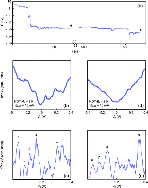 | ||
| Fig. 4 IETS analyses on HDT single molecule junctions at GH and GL. (a) G–t traces obtained under stretching at 6 pm s−1 at 4.2 K. IETS measurements were performed at points marked as “A” and “B” where conductance was close to GH and GL, respectively. (b, d) dI/dVb–Vb characteristics and (c, e) corresponding IET spectra obtained at the high- and low-G states, respectively. The peak marked with an asterisk cannot be assigned to any IETS-active molecular vibration modes. | ||
| Molecule | Peak no. | Peak position | HREELS (calculation) cm−1 | Vibration modes | |
|---|---|---|---|---|---|
| mV | cm−1 | ||||
| HDT-A | 1 | 38 | 307 | 220 (274) | ν(Au–S) |
| 2 | 82 | 662 | 650 (645) | ν(C–S) | |
| 3 | 120 | 969 | 1050 (1065) | ν(C–C) | |
| 4 | 163 | 1316 | 1300 (1365) | γw(CH2) | |
| 5 | 345 | 2785 | 2865 (3096) | νs(CH2) | |
| HDT-B | 6 | 33 | 266 | 220 (274) | ν(Au–S) |
| 7 | 81 | 654 | 650 (645) | ν(C–S) | |
| 8 | 137 | 1106 | 1050 (1065) | ν(C–C) | |
| 9 | 357 | 2882 | 2865 (3096) | νs(CH2) | |
After exploring d2I/dVb2–Vb characteristics at GH, we resumed junction stretching at vd = 6 pm s−1. Consequently, we observed a conductance jump from GH to GL and a subsequent plateau, which indicates a mechanically induced transition of an HDT single molecule junction from the high- to low-G state. We then conducted a lock-in measurement and obtained dI/dVb–Vb characteristics with step features analogous to those found at GH (Fig. 4(d)). The corresponding IET spectrum (Fig. 4(e)) reveals pronounced peaks at Vp = 33 mV and 81 mV, 137 mV, and 357 mV, which can all be assigned to the HREELS-active vibration modes of ν(Au–S), δr(CH2), ν(C–C), and νs(CH2), respectively. These spectroscopic fingerprints clearly suggest that both GH and GL states are of single HDT molecule origin.
It should be pointed out further that d2I/dVb2–Vb curves in Fig. 4(c, e) reproduce IET spectra of an alkanedithiol monolayer reported by several groups only partially.37–39 The discrepancy presumably stems from a difference in the number of molecules and accompanying variability in the metal–molecule–metal configurations involved. Metal–SAM–metal structures can be considered as an aggregation of molecular junctions with diverse geometries. IET spectra of molecular SAMs therefore represent an ensemble average of the configurational variations. In contrast, by analogy, single molecule IETS probes vibrational characteristics unique to a molecular junction with a particular metal–molecule–metal motif. This explains why the SAM-IET spectrum encompasses more than all the vibrational features detected here, which in turn verifies at the same time that MCBJ-IETS is indeed a sensitive probe of atom-scale structures of metal–molecule–metal systems.
Identification of HDT single molecule junction configurations
We now discuss a junction evolution mechanism responsible for a mechanical transition from the GH to the GL state presented in Fig. 4(a). In the literature, configuration-specific single molecule conductance in Au–alkanedithiol–Au systems is explained by the influence of intramolecular conformations in alkyl chains and adsorption structures of Au–S links on electron transmission.14–17 Theoretical examinations of IETS on model geometries provide a key tool for the spectroscopic identification of metal–molecule–metal configurations. Effects of metal–molecule contact configurations on IET spectra have been estimated by Kula and co-workers.32,40 The authors reported the enhanced relative intensity of ν(Au–S) and νs(CH2) features together with diminishing γw(CH2) contributions in the calculated IET spectra upon changing molecular adsorption sites of Au–alkanedithiol–Au bridges from hollow–hollow to top–top arrangements, the propensity of which was ascribed to discrepancy in orientations of molecular dipole moments arising from a change from straight to twisted molecular conformations.32,40 This tendency has actually been observed here; lowering of ν(Au–S) and γw(CH2) relative peak heights during GH to GL transition, along with the prominent νs(CH2) characteristics in the low-G spectrum are suggestive of deformations of Au–S contacts from hollow to top configurations.We statistically examined the reproducibility of the difference found in HDT single molecule IET spectra at GH and GL. About 50 IET spectra were acquired for HDT single molecule junctions at GH and GL states, and the positions of peaks observed in the spectra were investigated (Fig. 5(a, b)). The peak position histograms reveal several peaks that well-reproduce the IET spectra shown in Fig. 4(c, e) (Table 2). Most significantly, we observed the disappearance of the γw(CH2) peak at GL.
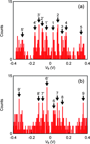 | ||
| Fig. 5 IETS peak position histograms of HDT single molecule junctions at (a) GH and (b) GL. Bin size is 0.004 V. | ||
| Molecule | Peak no. | Peak position/mV | Vibration modes |
|---|---|---|---|
| HDT-GH | 1 | 30 | ν(Au–S) |
| 1′ | −38 | ||
| 2 | 82 | ν(C–S) | |
| 2′ | −84 | ||
| 3 | 126 | ν(C–C) | |
| 3′ | −122 | ||
| 4 | 170 | γw(CH2) | |
| 4′ | −166 | ||
| 5 | 330 | νs(CH2) | |
| 5′ | −308 | ||
| HDT-GL | 6 | 42 | ν(Au–S) |
| 6′ | −36 | ||
| 7 | 76 | ν(C–S) | |
| 7′ | −84 | ||
| 8 | 130 | ν(C–C) | |
| 8′ | −124 | ||
| 9 | 336 | νs(CH2) | |
| 9′ | −357 |
Electronic coupling strength at metal–molecule linkages is known to play a significant role in electron transport in molecular junctions through shifting and broadening molecular energy levels; first principle calculations have revealed expansive distributions of single dithiol molecule conductance spanning orders of magnitude depending on its Au–S bonding geometry.11–13 We therefore speculate that the high- and low-G states of single HDT junctions stem from a difference in metal–molecule contact configurations.
The single molecule structural analyses have provided evidence that the mechanically controllable two-state conductance switching occurs via repeated deformations of the Au–S links between top and hollow motifs. Then, it is of practical interest whether the metal–molecule configurational switching can occur at GHz or beyond. Unfortunately, however, the reliable range of piezo-actuator motions in our experimental set up is limited to νp < 1 kHz, and hence beyond the scope of this study. Perhaps, electromechanical actuation using back-gated nano-MCBJs would allow the elucidation of the potential switching speed of the single molecule switch,41 work into which is now in progress.
Conclusions
We investigated the configuration-specific conductance and underlying characteristic geometries in Au–HDT–Au systems. Break junction measurements revealed two distinct single molecule conductance values of GH ∼ 1.3 mG0 and GL ∼ 0.4 mG0. Structural identifications via IETS analyses suggested that the high- and low-conductance states were attributable to HDT single molecule bridges with hollow–hollow and top–top adsorption motifs at the Au–S links respectively. We demonstrated a two-state HDT single molecule switch by controlling on/off through mechanical transitions of the bistable metal–molecule contact configurations, and thereby accomplished ultimate miniaturization of a switching device.Notes and references
- M. A. Reed, C. Zhou, C. J. Muller, T. P. Burgin and J. M. Tour, Science, 1997, 278, 252 CrossRef CAS.
- B. Xu and N. J. Tao, Science, 2003, 301, 1221 CrossRef CAS.
- M. Galperin, M. A. Ratner, A. Nitzan and A. Troisi, Science, 2008, 319, 1056 CrossRef CAS.
- S. Lindsay and M. A. Ratner, Adv. Mater., 2007, 19, 23 CrossRef CAS.
- H. Park, J. Park, A. K. L. Lim, E. H. Anderson, A. P. Alivisatos and P. L. McEuen, Nature, 2000, 407, 57 CrossRef.
- N. J. Tao, Nat. Nanotechnol., 2006, 1, 173 CrossRef CAS.
- J. E. Green, J. W. Choi, A. Boukai, Y. Bumimovich, E. Johnston-Halperin, E. Delonno, Y. Luo, B. A. Sheriff, K. Xu, Y. S. Shin, H.-R. -Tseng, J. F. Stoddart and J. R. Heath, Nature, 2007, 445, 414 CrossRef CAS.
- M. Elbing, R. Ochs, M. Koentopp, M. Fischer, C. von Hänisch, F. Weigend, F. Evers, H. B. Weber and M. Mayor, Proc. Natl. Acad. Sci. U. S. A., 2005, 102, 8815 CrossRef CAS.
- E. G. Emberly and G. Kirczenow, Phys. Rev. Lett., 2003, 91, 188301 CrossRef.
- S. Y. Quek, M. Kamenetska, M. L. Steigerwald, H. J. Choi, S. G. Louie, M. S. Hybertsen, J. B. Neaton and L. Venkataraman, Nat. Nanotechnol., 2009, 4, 230 CrossRef CAS.
- M. Di Ventra, S. T. Pantelides and N. D. Lang, Phys. Rev. Lett., 2000, 84, 979 CrossRef CAS.
- Z. Yang, N. D. Lang and M. Di Ventra, Appl. Phys. Lett., 2003, 82, 1938 CrossRef CAS.
- H. Basch, R. Cohen and M. A. Ratner, Nano Lett., 2005, 5, 1668 CrossRef CAS.
- X. Li, J. He, J. Hihath, B. Xu, S. Lindsay and N. J. Tao, J. Am. Chem. Soc., 2006, 128, 2135 CrossRef CAS.
- J. He, O. Sankey, M. Lee, N. J. Tao, X. Li and S. Lindsay, Faraday Discuss., 2006, 131, 145 RSC.
- M. Fujihira, M. Suzuki, S. Fujii and A. Nishikawa, Phys. Chem. Chem. Phys., 2006, 8, 3876 RSC.
- M. T. González, J. Brunner, R. Huber, S. Wu, C. Schonenberger and M. Calame, New J. Phys., 2008, 10, 065018 CrossRef.
- M. Tsutsui, Y. Teramae, S. Kurokawa and A. Sakai, Appl. Phys. Lett., 2006, 89, 163111 CrossRef.
- J. M. van Ruitenbeek, A. Alvarez, I. Pineyro, C. Grahmann, P. Joyez, M. H. Devoret, D. Esteve and C. Urbina, Rev. Sci. Instrum., 1996, 67, 108 CrossRef CAS.
- M. Tsutsui, K. Shoji, K. Morimoto, M. Taniguchi and T. Kawai, Appl. Phys. Lett., 2008, 92, 223110 CrossRef.
- M. Tsutsui, K. Shoji, M. Taniguchi and T. Kawai, Nano Lett., 2008, 8, 345 CrossRef CAS.
- M. Tsutsui, M. Taniguchi and T. Kawai, Nano Lett., 2009, 9, 2433 CrossRef CAS.
- H. Ohnishi, Y. Kondo and K. Takayanagi, Nature, 1998, 395, 780 CrossRef CAS.
- N. Agraït, A. L. Yeyati and J. M. van Ruitenbeek, Phys. Rep., 2003, 377, 81 CrossRef CAS.
- S. -Y. Jang, P. Reddy, A. Majumdar and R. A. Segalman, Nano Lett., 2006, 6, 2362 CrossRef CAS.
- Z. Huang, B. Xu, Y. Chen, M. Di Venra and N. J. Tao, Nano Lett., 2006, 6, 1240 CrossRef CAS.
- Z. Huang, F. Chen, R. D'agosta, P. A. Bennett, M. Di Ventra and N. J. Tao, Nat. Nanotechnol., 2007, 2, 698 CrossRef CAS.
- R. H. M. Smit, Y. Noat, C. Untiedt, N. D. Lang, M. C. van Hemert and J. M. van Ruitenbeek, Nature, 2002, 419, 906 CrossRef CAS.
- M. Taniguchi, M. Tsutsui, K. Yokota and T. Kawai, Nanotechnology, 2009, 20, 434008 CrossRef.
- M. Tsutsui, M. Taniguchi, K. Shoji, K. Yokota and T. Kawai, Nanoscale, 2009, 1, 164 RSC.
- A. Troisi and M. A. Ratner, Small, 2006, 2, 172 CrossRef CAS.
- J. Jiang, M. Kula, W. Lu and Y. Luo, Nano Lett., 2005, 5, 1551 CrossRef CAS.
- M. Kula, J. Jiang and Y. Luo, Nano Lett., 2006, 6, 1693 CrossRef CAS.
- M. Rahimi and A. Troisi, Phys. Rev. B: Condens. Matter Mater. Phys., 2009, 79, 113413 CrossRef.
- M. J. Frisch, G. W. Trucks, H. B. Schlegel, G. E. Scuseria, M. A. Robb, J. R. Cheeseman, J. A. Montgomery, Jr., T. Vreven, K. N. Kudin, J. C. Burant, J. M. Millam, S. S. Iyengar, J. Tomasi, V. Barone, B. Mennucci, M. Cossi, G. Scalmani, N. Rega, G. A. Petersson, H. Nakatsuji, M. Hada, M. Ehara, K. Toyota, R. Fukuda, J. Hasegawa, M. Ishida, T. Nakajima, Y. Honda, O. Kitao, H. Nakai, M. Klene, X. Li, J. E. Knox, H. P. Hratchian, J. B. Cross, V. Bakken, C. Adamo, J. Jaramillo, R. Gomperts, R. E. Stratmann, O. Yazyev, A. J. Austin, R. Cammi, C. Pomelli, J. Ochterski, P. Y. Ayala, K. Morokuma, G. A. Voth, P. Salvador, J. J. Dannenberg, V. G. Zakrzewski, S. Dapprich, A. D. Daniels, M. C. Strain, O. Farkas, D. K. Malick, A. D. Rabuck, K. Raghavachari, J. B. Foresman, J. V. Ortiz, Q. Cui, A. G. Baboul, S. Clifford, J. Cioslowski, B. B. Stefanov, G. Liu, A. Liashenko, P. Piskorz, I. Komaromi, R. L. Martin, D. J. Fox, T. Keith, M. A. Al-Laham, C. Y. Peng, A. Nanayakkara, M. Challacombe, P. M. W. Gill, B. G. Johnson, W. Chen, M. W. Wong, C. Gonzalez and J. A. Pople, GAUSSIAN 03 (Revision C.02), Gaussian, Inc., Wallingford, CT, 2004 Search PubMed.
- H. S. Kato, J. Noh, M. Hara and M. Kawai, J. Phys. Chem. B, 2002, 106, 9655 CrossRef CAS.
- W. Wang, T. Lee, I. Kretzschmar and M. A. Reed, Nano Lett., 2004, 4, 643 CrossRef CAS.
- J. G. Kushmerick, J. Lazorcik, C. H. Patterson, R. Shashidhar, D. S. Seferos and G. C. Bazan, Nano Lett., 2004, 4, 639 CrossRef.
- N. Okabayashi, Y. Konda and T. Komeda, Phys. Rev. Lett., 2008, 100, 217801 CrossRef.
- J. Jiang, M. Kula and Y. J. Luo, J. Phys.: Condens. Matter, 2008, 20, 374110 CrossRef.
- C. A. Martin, R. H. M. Smit, H. S. J. van der Zant and J. M. van Ruitenbeek, Nano Lett., 2009, 9, 2940 CrossRef CAS.
Footnote |
| † Electronic supplementary information (ESI) available: Fig. S1: Reproducibility of conductance histograms and Fig. S2: G–t curve selection criterion. See DOI: 10.1039/c0sc00129e |
| This journal is © The Royal Society of Chemistry 2010 |
