Synthesis and characterization of one-dimensional flat ZnO nanotower arrays as high-efficiency adsorbents for the photocatalytic remediation of water pollutants†
Da
Deng
,
Scot T.
Martin
and
Shriram
Ramanathan
*
Harvard School of Engineering and Applied Sciences, Cambridge, MA 02138, USA. E-mail: shriram@seas.harvard.edu
First published on 14th October 2010
Abstract
We report on facile fabrication of 1-D flat ZnO nanotower arrays on various substrates, including a metal, a semiconductor and an insulator. The nanotowers have a unique flat basal section near the substrate and taper in stages to wire-like at the tip. Electron microscopy and X-ray photoelectron spectroscopy are used to characterize these new nanostructures, revealing that their morphologies are significantly influenced by reaction temperature. A qualitative formation mechanism is proposed based on the experimental observations. A proof-of-concept demonstration shows that the ZnO nanotower arrays are highly effective at adsorbing and subsequently photo-remediating a model pollutant (Eosin B) from water. These observations could promote new applications of photocatalytic adsorbents for wastewater treatment utilizing oxide semiconductor nanostructures.
1. Introduction
ZnO-based materials have size and morphology dependent physical and chemical properties at the nanoscale which could offer tremendous opportunities for advanced technologies.1–3 For example, nanostructured ZnO is being actively explored in light-emitting diodes,4 laser diodes,5 sensors,6 pizeoelectronics,7,8 solar cells,9 UV-blocking components,10 photocatalysis,11–13 and transparent conductive glass coatings.14 Various kinds of 1-D ZnO nanostructures have been reported, ranging from uniform nanobelts,15 nanotubes16 to nanowires.17 It is known that the properties of nanostructured materials are size and shape dependent. Unique structures could introduce additional tunable properties. However, it is still challenging to fabricate nanoarrays such as those of 1-D ZnO with deterministic morphologies on chosen substrates by simple methods. While most of the reported 1-D ZnO have a near uniform diameter along the nanostructure length, nanostructures with non-uniform diameter or stages along the 1-D nanostructure length and associated asymmetrical physical properties may be of interest toward electronic, thermal and vibration transport control in future nanodevices. A simple method for large-scale and low-cost fabrication of 1-D ZnO nanostructures having non-uniform diameters on various substrates could be of potential interest for further studies of their functional properties. Here, we note that non-uniform 1-D ZnO nanotowers with hexagonal cross-sections have been reported previously.18–21 Preparation methods included high temperature (>950 °C) chemical conversion of ZnS,19 chemical bath despostion,21 thermal oxidization with controlled oxygen18 and two-step hydrothermal methods using ZnO seed layers.20In the context of semiconductor photocatalysts for water treatment, 1-D ZnO nanostructures could offer various advantages. Non-biodegradable dyes widely used in textile, paper and other industrials pose severe threats to aqueous environments when released without treatment. The elimination of harmful components (including dyes) from wastewater is an important goal for environmental control in industrial settings. Adsorption and chemical coagulation are traditionally used for the treatment of such wastewater.22 However, the traditional methods transfer dyes, and the solid waste containing dyes is hard to handle. On the other hand, semiconductor photocatalysts such as ZnO utilizing photo-induced oxidation process could decompose the dyes effectively.12,22
Both powder and thin film forms of ZnO have been explored to date for environmental applications.22,23 Powder-form ZnO semiconductor photocatalysts normally show higher photoefficiency due to the increased active surface area. However, the powder form photocatalysts used in suspension state in water have certain limitations due to particle aggregation and technical challenges in photocatalyst separation and recovery.24 In comparison, thin film ZnO can be easily recovered, yet its surface area is low leading to poor overall efficiency.11 In comparison, 1-D nanostructured ZnO arrays with high surface-to-volume ratio grown on substrates could offer advantages of both high surface area and easy recovery.25 Furthermore, due to the large surface area offered by 1-D ZnO nanoarrays, they could be efficient adsorbents. The adsorbed pollutants can be subsequently photocatalytically decomposed on the surface and the photocatalyst can be reused.
Here we report on the facile synthesis of 1-D ZnO flat nanotower arrays on various substrates by thermal oxidation. The substrates explored here include glass (insulator), a silicon wafer (semiconductor) and zinc metal foil (conductor). The 1-D ZnO has a unique tower like structure with flat basal section near the substrate and tapers in stages to wire-like at the tip. To test the absorptive and photocatalytic capacities of the ZnO nanotower arrays, we use the model dye wastewater pollutant Eosin B. This red dye, commonly used as a biological stain and stable in normal conditions, is harmful if swallowed, inhaled, or absorbed through skin, and has been used as a model dye in the evaluation of photocatalysis.12,26 The application of the these unique 1-D flat ZnO nanotower arrays as adsorbent and subsequently used for photocatalytic decomposition in air has not been previously reported to the best of our knowledge. For our proof-of-concept demonstration, the typical Eosin B absorbance peak at 518 nm can be readily monitored.
2. Results and discussion
FESEM images of ZnO nanotowers fabricated on glass slides at 550 °C are shown in Fig. 1. The low magnification image (Fig. 1a) viewed from the top shows that a dense array of ZnO nanotowers forms on the glass substrate. Each nanotower has a broad and flat basal section near the substrate which then narrows to a wire at the tip (Fig. 1b). In contrast to other reported 1-D ZnO nanoarrays,16 the ZnO nanotower arrays reported here are not perpendicular to the substrate but instead are tilted at 60° to 70°. Fig. 1c shows a high-magnification side view of the base region indicating flat morphology at the basal sections. The inset of Fig. 1c shows the corresponding low magnification view, revealing that a layer of ZnO thin film is formed on the glass slide. The flat tower morphology is evident in the high-magnification top view shown in Fig. 1d. The line highlighted by a white arrow emphasizes the contact between the nanotower and substrate. A typical ZnO nanotower characterized by stages is apparent in Fig. 1e. The nanotower arrays could also be fabricated with similar morphology on a semiconducting silicon wafer surface (see ESI, Fig. S1†). In addition to glass substrate and silicon wafer, similar ZnO nanotower arrays could be fabricated directly on Zn foil by thermal oxidation in air, as revealed by FESEM images at different magnification shown in Fig. S2, ESI†. Hence, such ZnO arrays can be fabricated on various substrates. Without Pd/Pt coating on glass slide or silicon wafer, flat ZnO nanotowers were not observed. This indicates that Pd/Pt coating could provide the wetting surface for deposition and nucleation of ZnO and 1-D growth.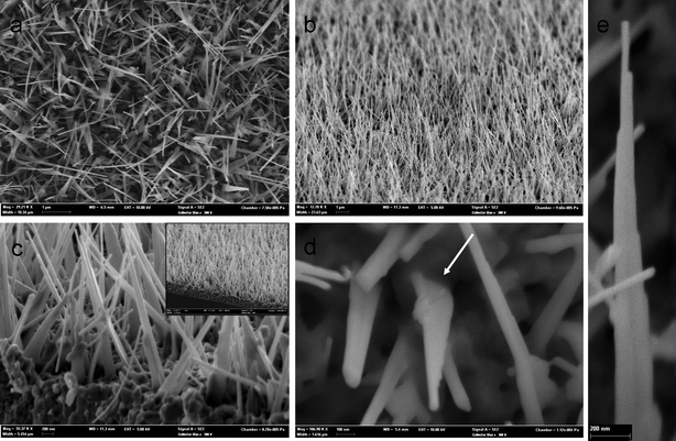 | ||
| Fig. 1 FESEM images of the 1-D flat ZnO nanotower arrays formed on glass slide substrate at 550 °C: (a) low magnification top view and (b) side view; (c) high magnification side view of the base of the ZnO nanotower arrays; the inset of (c) is the corresponding low magnification side view; (d) high magnification top view of a few nanotowers indicating flat structure; and (e) a typical ZnO nanotower with stages clearly observed. | ||
The XRD patterns (Fig. 2a) confirm that ZnO phase with wurtzite (hexagonal) structure are formed on both glass slide substrate and on the Zn foil upon thermal oxidation. The XRD peaks could be assigned according to JCPDS card no. 65-3411 for wurtzite. Fig. 2b shows a broad scan survey XPS spectrum of the ZnO arrays. The survey spectrum is typical of ZnO and the main photoelectron peaks can be assigned to Zn- and O-derived bands.27 Compared to Fig. 2b, Fig. 2c and d show high-resolution analysis. The O 1s band has a large asymmetry (Fig. 2c), corresponding to Gaussian components centered at 529 and 530.6 eV. The lower binding energy spectrum of the O 1s could be attributed to the O2− ions in the wurtzite structure of stoichiometric ZnO. The shift of O 1s to a higher binding energy indicates the presence either of point defects or chemisorbed oxygen, possibly as OH, H2O or –CO3.28 The high-resolution analysis of Zn 3s band shows high symmetry (Fig. 2d), which could be assigned to the Zn2+ ions in ZnO. The atomic ratio based on XPS analysis for O![[thin space (1/6-em)]](https://www.rsc.org/images/entities/char_2009.gif) :Zn also agrees with that of commercial ZnO powder analyzed by XPS.
:Zn also agrees with that of commercial ZnO powder analyzed by XPS.
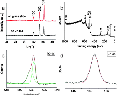 | ||
| Fig. 2 (a) XRD spectrum of the ZnO nanotower arrays fabricated on glass slide and Zn foil surface; (b) XPS spectrum of the ZnO nanotower arrays; and (c) high resolution of XPS spectrum of O 1s and (d) Zn 3s. | ||
The novel morphology of the ZnO nanostructures is vividly revealed by the TEM characterization shown in Fig. 3. A typical ZnO nanotower is shown in Fig. 3a at low magnification. The broad basal section narrows stage by stage toward the tip. The ripple-like contrast along the nanotower is typically observed for flat ZnO nanostructure.15 The high-resolution TEM (HRTEM) in Fig. 3c indicates that the nanotower is single crystalline, as further confirmed by selected-area electron diffraction (SAED) shown in the inset. The diffraction spots correspond to the wurtzite structure ZnO. The emphasized region in Fig. 3d shows a crystallinity having a d-spacing of 0.26 nm that matches well to the d(002) planes of wurtzite. The SAED collected at both the tip and basal sections of the nanotower shows similar patterns all indicating the ZnO nanotower growth in the direction perpendicular to [001]. This growth direction is different from previously reported non-flat ZnO nanotowers which were oriented along the [001] diection.19,20,29 Non-flat ZnO nanotowers reported in literature have hexagonal crosssection and are grown along c-axis; surrounded by equivalent facets of (101), (110), (011) to minimize energy.30 However, in our case, the c-axis is in-plane and the growth occurs by extension into a unique flat morphology likely to reduce the exposure of unstable (002) planes to minimize surface energy.20,31 This could qualitatively explain the difference between our flat ZnO nanotower to those literature reported ZnO nanotowers with hexagonal crosssection. Fig. 3e shows a typical nanotower having a branch on the shoulder and growing independently into another flat tower structure. Fig. 3f shows the ripple like contrast along a typical ZnO nanotower. A branched structure is formed at the top section for this nanotower.
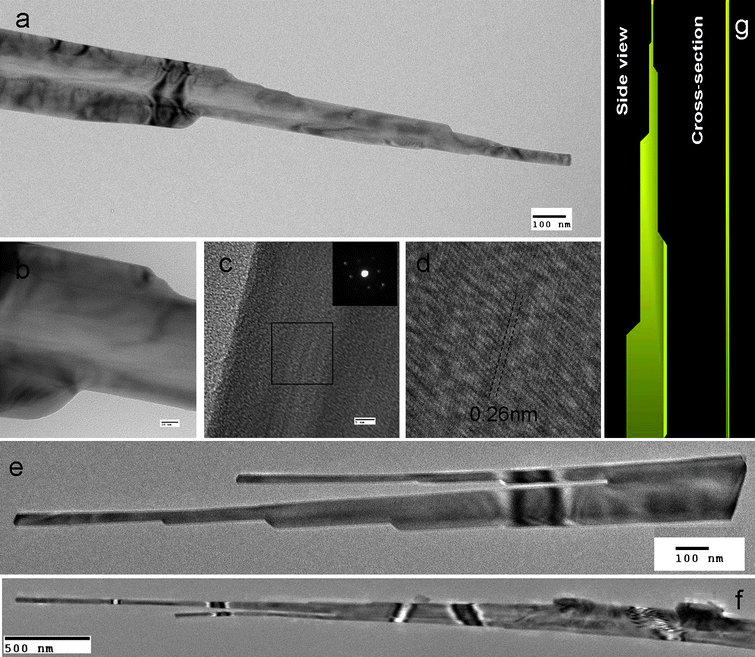 | ||
| Fig. 3 TEM images of the ZnO nanotowers: (a) the stages in the flat nanotower clearly observed in the low magnification image; (b) high magnification view of the stages; (c) HRTEM image of the nanotower and the inset showing a selected area diffraction pattern; (d) close-up view of the area highlighted in (c) clearly shows the single crystal structure; (e) ZnO nanotower with branch at the basal section; (f) a typical ZnO nanotower with ripple like contrast and branch at the tip section; and (g) illustration to show the structure. | ||
The experimental results of Fig. 4 demonstrate that the fabrication temperature strongly influences the morphology of the 1-D ZnO nanotower arrays. At 650 °C, the nanotowers formed on Zn foil substrate broaden and increase in length compared to those of lower temperatures. The stages are also less clearly differentiated, approaching the structure of a needle (Fig. 4a). Fig. 4c shows a typical ZnO nanotower fabricated at 650 °C, with the tip and basal sections of this ZnO tower enlarged in Fig. 4d and 5e. In addition to the aspect ratio, the “base-to-tip” ratio, which is the ratio of the width of the basal section to tip section, is ∼28:1. The ZnO nanotower structure also can be grown on a glass substrate at 650 °C, as expected and shown in Fig. 4b. At 400 °C, ZnO nanowires form primarily (Fig. 4f and g).
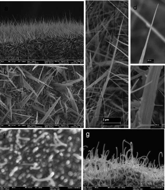 | ||
| Fig. 4 FESEM images of the ZnO nanotowers fabricated on Zn foil at 650 °C for 2 h: (a) low magnification view of the ZnO nanotowers; (b) ZnO nanotowers fabricated on glass slide at 650 °C; (c) ZnO nanotower with high aspect ratio; (d and e) the zoom-in view of the basal and tip region of highlighted in c shows a large “base-tip ratio”; (f) the initial stage of growth with nanoparticles and (g) ZnO nanowires formed at 400 °C. | ||
 | ||
| Fig. 5 Schematic diagram showing the proposed growth steps for ZnO nanotowers. | ||
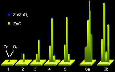
Based on the above characterization and analysis, we qualitatively propose a formation mechanism for the ZnO nanotower, as illustrated in Fig. 5. At the initial stage of thermal oxidation, implying a high concentration of Zn, a thin layer of ZnO is present on the substrates (i.e., glass slide or silicon wafer). For the case of Zn foil, ZnO grows by oxidation at the surface. For the glass slide and the silicon wafer, ZnO is formed by the condensation of Zn onto the Pd/Pt wetted surface, followed by oxidation. Zn/ZnOx clusters then form on the surface (step 1), functioning as nucleation sites for further deposition. The initial stage formation of nanoparticles was experimentally observed as shown in Fig. 4f. With the continued supply of evaporated Zn from metal source and O2 from air at the high temperature, ZnO starts to adsorb on the surface of the clusters and further deposits at the interface of the Zn/ZnOx, eventually growing as a nanowire (step 2). The formation of nanowires was experimentally observed as shown in Fig. 4g. The ZnO adsorbed on the tip of the nanowire promotes further vertical growth, while the ZnO adsorbed on the side of the nanowire causes lateral growth. Due to higher concentrations at the base, additional nucleation and growth occur (step 3) and continue in subsequent stages (step 4). This is experimentally observed in Fig. 4b. Since the Zn/ZnOx structures are exposed to air at high temperature, they can be oxidized to ZnO, forming a nanotower (step 5). A fully grown nanotower is illustrated in Fig. 5a. For the branched 1-D flat ZnO nanotower, the excess supply of Zn at the basal section could promote the formation of additional structures. Subsequently, it forms a branch, as illustrated in 6b and as observed experimentally. Detailed studies at the initial stages of growth are required to fully understand the nanowire growth mechanism.
A proof-of-concept demonstration was carried out for the potential use of the ZnO nanotower arrays as photocatalytic adsorbents. Fig. 6a shows the ultraviolet-visible (UV-Vis) spectra of an Eosin dye solution for progressive contact times with ZnO nanotower arrays (without UV exposure). The absorbance decreases continuously over time, indicating that the ZnO nanotower arrays effectively adsorb the dye from the solution. There are no other absorbance peaks observed, indicating that the process is physical sorption with no new chemical components generated. The mechanism of dye adsorption could be similar to that of activated carbon with large surface area for surface adsorption.22,32Fig. 6b shows the normalized concentration of the dye in solution decreases with time, with ∼80% loss of dye from solution over 350 min for the first run of adsorption. For comparison, we tested a ZnO thin film that did not have a nanotower morphology: it was fabricated on Zn foil by heating a zinc foil substrate on hot plate for several hours. In the case of this lower surface area thin film, only 10% of the dye was adsorbed over a similar 350 min period. Fig. 6c shows the gradual decrease in color of the solution (upper) and gradual increase of the color of the ZnO nanotower arrays (lower).
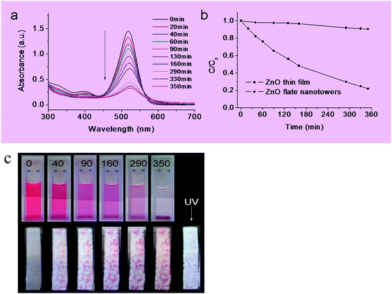 | ||
| Fig. 6 Proof-of-concept demonstration of the 1-D flat ZnO nanotower arrays as a recoverable and reusable photocatalytic adsorbent in an environmental application for the remediation of a dye pollutant in water: (a) UV-Vis spectra of the eosin B measured for increasing adsorption times; (b) normalized concentration for increasing adsorption time (no UV exposure) for a fresh ZnO nanotower arrays; results are compared to a ZnO thin film prepared by conventional methods; and (c) optical images of the change in color of the solution (upper) and the corresponding ZnO materials (lower) over time corresponding to the data of panels (a) and (b); the right most image in the lower panel shows that the ZnO nanotower arrays are photo-bleached after exposure to UV radiation for 30 min; this recovered sample was subsequently used for the second run. | ||
Upon exposure to ultra-violet radiation, the adsorbed red dye on the surface was decomposed. The white photo-bleached sample is shown in the lower-right of Fig. 6c. As a control experiment, exposure to UV radiation alone without any ZnO present did not cause dye decomposition, in agreement with earlier reports.26 The mechanism of dye decomposition on the ZnO nanotower arrays is based on the redox reactions that occur on the semiconductor surface, as promoted by the photo-induced electron–hole separation.22,25,33 ZnO has a band gap of 3.2 eV, corresponding to an onset excitation of 380 nm. A photon promotes electrons from the valence band to the conduction band, creating a hole in the valence band. The electron–hole pairs can recombine in the volume or at the surface to unproductively release heat or alternatively can interact with surface-adsorbed molecules to induce chemistry. With the presence of oxygen as an electron donor, the dye adsorbed can be oxidized and possibly mineralized on the semiconductor surface via common photocatalysis process (although we do not have any direct evidence for this in the present work).33,34 The restore of the surface color of the ZnO nanoarrays covered substrate observed experimentally indirectly evidenced the mineralization of the adsorbed dye. After photo-exposure, the initial white color of the ZnO nanotower arrays returns (Fig. 6c), and the recovered arrays are reusable for further adsorption and photocatalysis. The second test run shows that the arrays are effective in adsorbing the dye (Fig. S3, ESI†).
3. Conclusions
A thermal oxidation method was employed to fabricate ZnO nanotower arrays on various substrates. The novel structure of the flat towers was characterized by electron microscopy (SEM/TEM), XRD and XPS. A qualitative formation mechanism for the nanotowers was proposed. The ZnO nanotower arrays served as an effective adsorbent for removing the model dye pollutant Eosin B from water. Following adsorption, the dye was decomposed on the surface by the redox reactions induced by ultraviolet illumination. We anticipate that these initial results could stimulate further studies on the exploration of solid state ZnO nanostructures for water treatment.4. Experimental
ZnO nanotower arrays synthesis
For the fabrication of ZnO nanotowers on glass slide (or silicon wafer), a piece of microscope cover glass slide (1 × 1 cm2) coated with Pt/Pd (80:20) target using Cressington 208HR sputter coater was used as a substrate. Zn foil (0.2 × 1.2 cm2, Sigma 99.9%) was placed in a crucible boat and partially covered with the glass slide with the Pt/Pd coated side facing downward to Zn foil. The crucible boat was transferred to a tube furnace and heated to desired temperature. For the fabrication of ZnO nanotowers on Zn substrate, the Zn foil was heated directly to the desired temperature and collected without any further treatment. The surface turned to grey in color indication the successful fabrication of ZnO nanotowers.
Materials characterization
The 1-D ZnO nanostructures were characterized by high resolution field-emission scanning electron microscopy and energy dispersive X-ray spectroscopy (FESEM/EDS, Supra55VP/Ultra55, Zeiss, Germany), transmission electron microscopy and selected-area electron diffraction (TEM/SAED, JEOL JEM-2100 operating at 200 kV), powder X-ray diffraction (XRD) on a Scintag XDS2000 X-ray diffractometer using Cu Kα radiation, and X-ray photoelectron spectroscopy (XPS) performed on a surface science SSX-100 spectrometer using monochromated Al-Kα X-rays and calibrated to a C 1s electron peak at 284 eV.Photocatalytic adsorbent evaluation
A piece (0.5 × 2.5 cm2) of Zn foil covered with ZnO nanotower arrays prepared by thermal oxidation was placed in a cuvette containing the model polluted water with 3 × 10⁻⁵ M Eosin B dye. The cuvette was then placed in dark. The concentration of Eosin B was monitored at different time intervals by an Agilent 8453 UV-Visible spectrophotometer using the absorbance peak of Eosin B at 518 nm. As adsorption occurred, the red color faded from the solution in the cuvette while the red coloring of the ZnO nanotower arrays saturated over time. The red stained samples could be reused after exposure to UV-Vis light from a 150 W UV-enhanced Xenon lamp to completely decompose the adsorbed Eosin B, restoring the surface to a white color.References
- Z. Y. Fan and J. G. Lu, J. Nanosci. Nanotechnol., 2005, 5, 1561 CrossRef CAS.
- C. Klingshirn, Phys. Status Solidi B, 2007, 244, 3027 CrossRef CAS.
- C. Klingshirn, ChemPhysChem, 2007, 8, 782 CrossRef CAS.
- S. J. Chen, Y. C. Liu, C. L. Shao, R. Mu, Y. M. Lu, J. Y. Zhang, D. Z. Shen and X. W. Fan, Adv. Mater., 2005, 17, 586 CrossRef CAS.
- H. K. Liang, S. F. Yu and H. Y. Yang, Appl. Phys. Lett., 2010, 96, 101116 CrossRef.
- J. Zhou, Y. D. Gu, P. Fei, W. J. Mai, Y. F. Gao, R. S. Yang, G. Bao and Z. L. Wang, Nano Lett., 2008, 8, 3035 CrossRef CAS.
- X. D. Wang, J. H. Song, J. Liu and Z. L. Wang, Science, 2007, 316, 102 CrossRef CAS.
- Z. L. Wang and J. H. Song, Science, 2006, 312, 242 CrossRef CAS.
- I. Gonzalez-Valls and M. Lira-Cantu, Energy Environ. Sci., 2009, 2, 19 RSC.
- N. Serpone, D. Dondi and A. Albini, Inorg. Chim. Acta, 2007, 360, 794 CrossRef.
- J. L. Yang, S. J. An, W. I. Park, G. C. Yi and W. Choi, Adv. Mater., 2004, 16, 1661 CrossRef CAS.
- C. H. Ye, Y. Bando, G. Z. Shen and D. Golberg, J. Phys. Chem. B, 2006, 110, 15146 CrossRef CAS.
- F. Xu, P. Zhang, A. Navrotsky, Z. Y. Yuan, T. Z. Ren, M. Halasa and B. L. Su, Chem. Mater., 2007, 19, 5680 CrossRef CAS.
- D. R. Sahu, S. Y. Lin and J. L. Huang, Appl. Surf. Sci., 2007, 253, 4886 CrossRef CAS.
- Z. W. Pan, Z. R. Dai and Z. L. Wang, Science, 2001, 291, 1947 CrossRef CAS.
- H. D. Yu, Z. P. Zhang, M. Y. Han, X. T. Hao and F. R. Zhu, J. Am. Chem. Soc., 2005, 127, 2378 CrossRef CAS.
- S. Xu, Y. Ding, Y. G. Wei, H. Fang, Y. Shen, A. K. Sood, D. L. Polla and Z. L. Wang, J. Am. Chem. Soc., 2009, 131, 6670 CrossRef CAS.
- J. Xiao, X. X. Zhang and G. M. Zhang, Nanotechnology, 2008, 19, 295706 CrossRef.
- P. A. Hu, Y. Q. Liu, L. Fu, X. B. Wang and D. B. Zhu, Appl. Phys. A: Mater. Sci. Process., 2005, 80, 35 CrossRef CAS.
- Y. H. Tong, Y. C. Liu, C. L. Shao and R. X. Mu, Appl. Phys. Lett., 2006, 88, 123111 CrossRef.
- N. Saleema and M. Farzaneh, Appl. Surf. Sci., 2008, 254, 2690 CrossRef CAS.
- S. Chakrabarti and B. K. Dutta, J. Hazard. Mater., 2004, 112, 269 CrossRef CAS.
- A. Mills and S. LeHunte, J. Photochem. Photobiol., A, 1997, 108, 1 CrossRef CAS.
- L. K. Adams, D. Y. Lyon and P. J. J. Alvarez, Water Res., 2006, 40, 3527 CrossRef CAS.
- T. J. Kuo, C. N. Lin, C. L. Kuo and M. H. Huang, Chem. Mater., 2007, 19, 5143 CrossRef CAS.
- J. S. Hu, L. L. Ren, Y. G. Guo, H. P. Liang, A. M. Cao, L. J. Wan and C. L. Bai, Angew. Chem., Int. Ed., 2005, 44, 1269 CrossRef CAS.
- J. F. S. Moulder, W. F. Stickle, P. E. Sobol and K. D. Bomben, Handbook of X-ray Photoelectron Spectroscopy, Perkin-Elmer Corporation, 1992 Search PubMed.
- P. T. Hsieh, Y. C. Chen, K. S. Kao and C. M. Wang, Appl. Phys. A: Mater. Sci. Process., 2008, 90, 317 CAS.
- Y. Liang, X. T. Zhang, L. Qin, E. Zhang, H. Gao and Z. G. Zhang, J. Phys. Chem. B, 2006, 110, 21593 CrossRef CAS.
- J. P. Liu, X. T. Huang, Y. Y. Li, X. X. Ji, Z. K. Li, X. He and F. L. Sun, J. Phys. Chem. C, 2007, 111, 4990 CrossRef CAS.
- Z. Wang, X. F. Qian, J. Yin and Z. K. Zhu, Langmuir, 2004, 20, 3441 CrossRef CAS.
- M. F. F. Sze and G. McKay, Environ. Pollut., 2010, 158, 1669 CrossRef CAS.
- M. R. Hoffmann, S. T. Martin, W. Y. Choi and D. W. Bahnemann, Chem. Rev., 1995, 95, 69 CrossRef CAS.
- Y. H. Zheng, C. Q. Chen, Y. Y. Zhan, X. Y. Lin, Q. Zheng, K. M. Wei, J. F. Zhu and Y. J. Zhu, Inorg. Chem., 2007, 46, 6675 CrossRef CAS.
Footnote |
| † Electronic supplementary information (ESI) available: SEM images of ZnO nanotowers on wafer and zinc substrates; 2nd run adsorption test. See DOI: 10.1039/c0nr00537a |
| This journal is © The Royal Society of Chemistry 2010 |