Recent advances in DNA-based directed assembly on surfaces
Albert M.
Hung
,
Hyunwoo
Noh
and
Jennifer N.
Cha
*
Department of Nanoengineering, University of CA, San Diego, USA. E-mail: jencha@ucsd.edu
First published on 13th September 2010
Abstract
In the last decade, “small” and “integrated” have been keywords in the field of device fabrication as the desire to exploit nanoscale phenomena and make electronic, photonic and magnetic arrays has grown. In an effort to improve resolution and control costs, much work has been dedicated to developing alternatives to conventional microfabrication technology. For this purpose, biomolecular assembly and DNA nanotechnology in particular are appealing owing to their inherent size and capacity for molecular recognition. Herein, we review recent achievements in DNA-based directed assembly on substrates. These include novel methods for patterning and depositing nanomaterials on DNA-modified surfaces as well as using synthetic DNA nanostructures such as DNA tiles and origami as templates to direct the assembly of nanoscale components. Particular attention is paid to integrating self-assembly with top-down lithography, and some possible directions for future work are discussed.
 Albert M. Hung | Albert M. Hung received his PhD in materials science and engineering in 2007 from Northwestern University where he was awarded a NDSEG Fellowship and a NSF Graduate Research Fellowship. He spent a year as a postdoctoral researcher at IBM Almaden Research Center before joining Prof. Cha as a postdoctoral researcher in the Department of Nanoengineering at UCSD. His research interests include the directed assembly and patterning of nanomaterials. |
 Hyunwoo Noh | Hyunwoo Noh is currently a graduate student in Prof. Jennifer Cha's group in the Department of Nanoengineering at UCSD. His research is focused on the use of biological materials, including DNA to direct the assembly of nanoscale objects. He received his Bachelors and Masters degrees in materials science and engineering in 2006 and 2008 respectively from Korea University. |
 Jennifer N. Cha | Jennifer N. Cha is currently an assistant professor in the Department of Nanoengineering at UC San Diego. Prior to this, Prof. Cha was a research staff member at the IBM Almaden Research Center in San Jose, CA. She received her PhD in Materials Chemistry from UC Santa Barbara in 2001. |
Introduction
Miniaturization has always been a goal of device designers. But the elucidation of nanoscale phenomena with the increasing demand for higher-performance processors and sensors has driven unprecedented interest in scaling down device features as much as possible. While top-down lithographic techniques, photolithography in particular, have been the workhorse of commercial microfabrication, physical and financial limitations of decreasing feature sizes has driven the investigation of a number of emerging technologies, including the use of self-assembled materials that can access very small length scales and exhibit thermodynamically stable, short-range order with minimal intervention. Biomolecules and bio-inspired assembly have been of particular interest in recent years because unlike many self-assembling systems such as block copolymers, colloids, and anodic aluminium oxide, they offer a greater propensity for specific molecular recognition and a method for “directed” assembly of nanoscale materials into desired device geometries. DNA is an especially elegant biological system that might prove useful in this regard.1–4 Compared to proteins that can be made of twenty different amino acids and for which the rules of folding, aggregation, and target recognition can be exceedingly complex, DNA is comprised of only four nucleic acids and assembles into well-known helical structures. Because the rules governing DNA hybridization are simpler, binding affinities and structure formation are more predictable and can be tuned by rational design of the DNA sequence. The characteristic length scales of the double helix, roughly 2 nm in width and 0.34 nm between bases, suggest that DNA-based assemblies could potentially be made with very high resolution.Since Seeman first suggested using DNA to build complex nanostructures nearly thirty years ago,5 major advances have be made in understanding how to exploit the singular properties of DNA to both create unique DNA structures and use them to assemble nanoparticles and nanowires. In just the last decade, the field of functional, synthetic DNA nanostructures has grown dramatically, as has interest in using DNA to fabricate nanometre-scale devices and sensors. A number of one- and two-dimensional (2D) DNA-based objects and lattices have been designed and assembled, some with breadboard-like capabilities that offer the opportunity to rationally direct nanocomponent assembly on surfaces. Even more exotic DNA constructs have been demonstrated including three-dimensional (3D) objects2,4 and nanomachines6 that are beyond the scope of this review.
Despite all of the progress in bio-nanofabrication, lithographic techniques cannot be rendered obsolete. In order to utilize DNA scaffolds for applications such as data storage, diagnostic assays, and electronic, optical, or plasmonic circuitry, the DNA structures will need to be placed on substrates with predetermined positional and rotational alignment and be used to further direct the assembly of nanoscale objects. Traditional lithographic methods may be adapted to pattern DNA for this purpose. Alternatively, a number of non-conventional lithographic techniques7 such as microcontact printing8 and dip-pen nanolithography (DPN)9 have also proven to be versatile and benign methods for patterning soft matter. The ability to integrate top-down lithography with bottom-up biological self-assembly is a growing avenue of research, several aspects of which will be highlighted in this review.
DNA-modified surfaces and particles
The most straightforward way of using DNA for directed self-assembly on surfaces is to first pattern the DNA on the substrate in the desired arrangement and then use it to bind or nucleate other materials. Surface modification with DNA can be achieved in a variety of ways. Conventional top-down methods such as photolithography and electron-beam lithography can be used to pattern a resist layer on a substrate which is then treated with DNA solutions. The DNA attaches only to the exposed areas of the surface via metal-thiol bonds or covalent chemistries such as silane or amide bonds.10–12 However, with the current scaling limitations of conventional lithography, it has remained difficult using such techniques to pattern very high resolution features of DNA in a cost-effective manner. As an alternative, methods such as DPN,13 nanografting,14 and scanning near-field photolithography15 which are based on material addition or subtraction via a scanning probe tip can also be used to pattern DNA. Nanografting can generate features as small as 10 nm, five to ten times smaller than DPN, but DPN doesn't require a resist layer and can readily create patterns of different DNA strands. More recently, inkjet printing employing electrohydrodynamic forces rather than thermal or mechanical energy was used to print DNA arrays for nanoparticle binding and aptamer-based biosensing (Fig. 1a).16 This technique offers slightly less resolution (approaching 100 nm) but works in non-contact mode which risks less damage to either probe or substrate. One of the major obstacles of either DPN or inkjet printing is that they remain serial processes that can be time-consuming for large area patterning.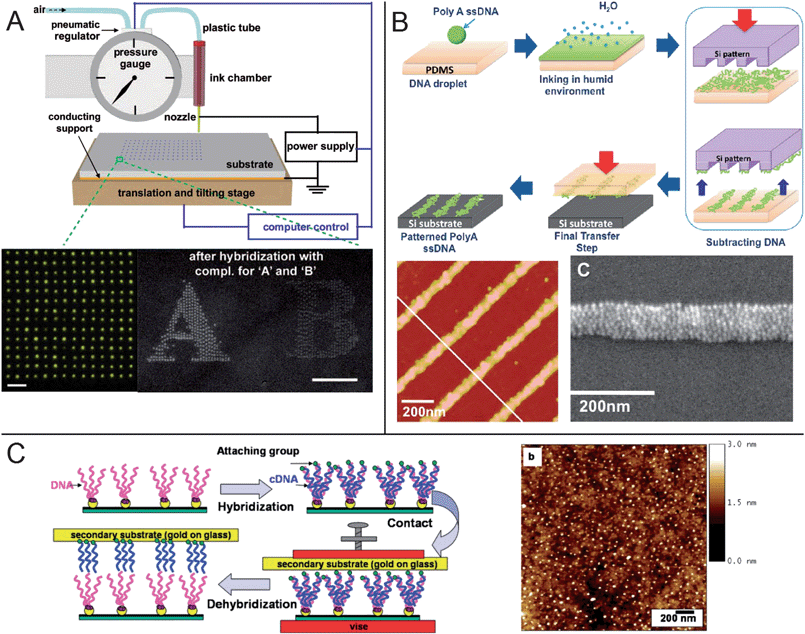 | ||
| Fig. 1 Methods for patterning of surfaces with DNA. (a) Electrohydrodynamic inkjet printing of DNA dot arrays. Two different DNA strands were printed as the letters “A” and “B” and selectively hybridize with 13 nm and 5 nm DNA-coated gold nanoparticles, respectively.16 Scale bars: 10 μm (left image) and 100 μm. (b) The ISP method was used to print lines of DNA approaching 50 nm that were then shown to be able to bind 10 nm gold nanoparticles.27 (c) Supramolecular printing was used to print complementary replicas of DNA arrays with features as small as 14 nm.34 | ||
Soft lithography encompasses another class of methods that are popular for patterning soft materials over large areas on arbitrary substrates using mild conditions.17 These techniques commonly employ a topographically patterned elastomeric poly(dimethyl siloxane) (PDMS) stamp to either transfer matter, as in microcontact printing, or to mold a material film, as in soft embossing. While these methods are limited in their resolution and feature density by what can be made by top-down lithography, they remain attractive because the expensive step of creating the topographical master pattern needs only to be done once, after which replicas of the pattern can be printed off the master multiple times and in a parallel fashion. Microcontact printing is among the most widely used soft lithographic techniques, although printing of DNA often requires greater consideration of hydration and electrostatic forces than printing of proteins.18 Recently, a microcontact printed surface pattern of DNA was used to bind 100 nm polystyrene spheres functionalized with complementary strands.19 The binding was proven to be reversible and sequence specific, two useful properties of DNA that are often not demonstrated in similar studies. In a different approach, DNA-coated gold nanoparticles were molded into patterned arrays upon drying from solution underneath a PDMS stamp.20 This study did not take advantage of DNA hybridization to tune nanoparticle assembly, although recent work has hinted at this possibility.21–24
One drawback of soft lithography is that because the elastomer is very soft, any small topographical features patterned on the stamp are very susceptible to deformation that limits resolution. It may also be difficult to transfer the DNA “ink” or to prevent spreading of the ink on contact with the surface. To overcome these and other limitations, new variations on soft lithographic methods are developed regularly. One idea for achieving higher resolutions is to spot the DNA on a flat, highly stretched stamp.25 When the stamp relaxes, the DNA array shrinks based on the size of the initial pattern and the applied strain. Another option is an “ink-subtract-print” (ISP) method wherein the organic material is first deposited as a film on a flat PDMS stamp.26 The inked stamp is then brought into contact with an etched silicon master which removes or “subtracts” material from the areas of contact, leaving a patterned film that can be transferred to a desired substrate. Proteins and DNA oligonucleotides have been patterned using the ISP approach to generate features approaching 50 nm. The DNA arrays were further used to bind single stranded (ssDNA) DNA-coated gold nanoparticles in tightly packed arrays (Fig. 1b).27
Most soft lithographic techniques are unable to print multiple different DNA sequences at once on a single substrate, making it difficult to take advantage of DNA's information encoding ability to build multicomponent structures. An interesting way around this problem is to use electric fields to spatially control hybridization regardless of DNA sequence,28 but this first requires patterning the electrodes. Instead, the sequence-specific and reversible binding of DNA can be harnessed to replicate a DNA monolayer onto another surface via affinity contact printing, a variant of microcontact printing that makes additional use of supramolecular interactions.29,30 A pattern of ssDNA is first tethered to a substrate or a stamp and is then hybridized to complementary strands added from solution31 or polymerized in situ by PCR.32 When a second surface is brought into contact with the pattern, the complements attach to it through end-functional binding groups31,32 or electrostatic interactions33 and are pulled off. This method allows multiple unique DNA strands to be replicated at once instead of having to print each strand separately for each substrate. Features as small as 14 nm have been printed in this way (Fig. 1c),34 limited primarily by the resolution of the initial pattern and the length of the DNA sequence.
While relatively short DNA strands are more commonly used for patterning and functionalizing surfaces, long DNA strands can also be employed to template material deposition. Usually, λ-DNA or other long double stranded DNA (dsDNA) chains are first aligned on a surface by electric fields, laminar flow, or drying front combing, as reviewed elsewhere.35 While most alignment methods cannot control the positioning of individual fibers, Guan and Lee produced well-ordered arrays of aligned λ-DNA by drying front combing on a topographically patterned PDMS stamp.36 DNA strands extended exclusively between or over regularly spaced recesses, and the array could also be transferred with controlled orientation to a second surface by contact printing. Elongated dsDNA can be used directly to template the nucleation and growth of nanowires of semiconductors and metals3,35 or to align carbon nanotubes (CNTs)37 or gold nanoparticle chains by electrostatic interactions.38 Metallization or non-specific adsorption often ignores any information stored in the DNA itself, but introducing proteins,39 reactive groups,40 or nanoparticles conjugated with short complementary sequences41 along the DNA strand may allow for site-selective nucleation or inhibition of material deposition, as demonstrated by the DNA templating of a CNT transistor.39 Recently, preferential nucleation of silver by cytosine versus thymine residues was also shown.42 The incorporation of metal ion-chelating sites within individual DNA strands and nanostructures is another strategy that can be used for localized control of chemical reactions and magnetic, electrical, or optical properties.43,44 Improvements in the quality of the nanowires obtained or the ability to deposit multiple materials would increase the utility of direct metallization.
DNA objects and tiles
In nature, DNA is not limited to forming simple linear helices but can also form links and junctions. Rationally designed DNA oligonucleotide sequences can thus make similar junctions to synthesize unique, 2D DNA subunits or “tiles.”2,4 These tiles are usually encoded with sets of extended ssDNA “sticky” strands that allow them to link with each other to create larger DNA scaffolds. In order to improve the assembly yield, information about the helical structure of DNA such as pitch and bond lengths must be taken into account such that there are no undue stresses and that the final assembled structure is thermodynamically stable. There currently exists a variety of computer programs to assist in the modeling and design of DNA tiles, and a myriad of interesting DNA structures have already been demonstrated that have potential use as templates to direct nanomaterial placement and assembly on surfaces.In general, DNA tiles are tens of nanometres in size and usually have rectilinear or hexagonal symmetry in order to efficiently pack and assemble over a larger surface. They can either be branched and assemble into open lattices, or they can possess a more compact shape and assemble into denser 2D DNA mats. By modifying sequences in the tiles so as to extend loose strands of ssDNA, nanoparticles functionalized with complementary strands can be bound to and arrayed on these lattices and mats.45,46 Alternatively, nanoparticles can be directly incorporated into the tiles in a single pot synthesis by first functionalizing each particle with a single strand of DNA used to form the junction.47,48 While the latter route tends to offer better control of nanoparticle spacing, this method is more labor intensive since it is difficult to generate monofunctionalized nanoparticles in high yields. These techniques have been used to direct the assembly of gold nanoparticles of up to two different sizes into nanometre-scale 2D periodic arrays that may have applications for electronic or plasmonic devices (Fig. 2a). Employing ligands with multiple thiol bonds improves the stability and subsequent binding yields of both gold and silver nanoparticles to DNA structures.49,50 Other functionalities such as biotin-streptavidin,51–53 aptamers,54 and antibody binding55,56 have also been employed to pattern materials besides gold, including fullerenes,57 quantum dots,51 and proteins.52–56 Furthermore, component binding can sometimes influence the structure of the DNA assembly and produce unique structures such as spiral chains of gold particles on DNA tubes58 and 2D DNA lattices that change symmetry upon binding of certain proteins.59
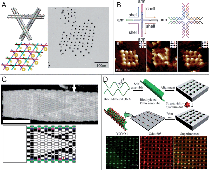 | ||
| Fig. 2 Directed assembly of nanocomponent arrays using DNA tiles. (a) 5 nm and 10 nm gold nanoparticles monofunctionalized with DNA were incorporated into triangular DNA tiles and assembled into a 2D array.48 (b) Cross-shaped DNA tiles assembled as finite, 16-tile grids.67 Individual tiles were modified to bind streptavidin to spell the letters D, N, and A. (c) Algorithmic assembly of a Sierpinski triangle pattern of “double-crossover” (DX) tiles nucleated from a DNA origami.70 Hairpin DNA loops on some tiles are used to visualize the pattern. Scale bar: 100 nm. (d) DNA tubules were aligned and arrayed on a patterned PDMS stamp by drying front combing and then used to bind streptavidin-functionalized quantum dots.73 The tubules were subsequently transferred onto a glass substrate by contact printing. Scale bars: 20 μm. | ||
DNA tiles are not limited to 2D arrangements but can also form elongated ribbons or finite objects. Ribbon or tube-like structures are obvious candidates for synthesizing nanowires through direct metallization of the DNA strands60,61 or assembling long chains of nanoscale components.62,63 Recently, DNA tubes were designed for both internal loading and selective release of encapsulated nanoparticles.64 The ability to control the width of DNA ribbons can also enable new uses,65 and functionalized DNA ribbons were recently employed to topologically control enzymatic cascades.66 Within a finite 2D scaffold composed of a discrete number of DNA tiles, each tile may be unique, and modification of individual tiles can lead to complex arrangements of organic and inorganic moieties, including spelling “D,” “N,” and “A” from streptavidin proteins (Fig. 2b)67 and assembling clusters of gold nanoparticles with well-defined geometries into modular and switchable arrangements.68 Individual tiles can also be designed such that they assemble in an algorithmic manner depending on tiles that have previously assembled, as was demonstrated by the seeded growth of a Sierpinski triangle pattern (Fig. 2c).69,70 Pattern information can be imparted by design of the nucleating seed as well.71 These capabilities extend the realm of possibility beyond simple rectilinear or hexagonal arrays to more complex arrangements.
The examples given so far demonstrate the capability and ease with which DNA tiles can arrange matter in an orderly fashion with better than 20 nm resolution over distances of micrometres. Despite these achievements, obtaining registry across tens of microns or more from DNA tiles remains a challenge. While it is possible to adsorb clusters of DNA tiles to patterned surfaces depending on the surface chemistry and ionic strength of the buffer, the DNA subunits are typically too small to be positioned and aligned individually.72 The extended 2D structures assembled from such subunits are often unbounded and are thus difficult to reliably pattern because there is no consistency to their shape. In contrast to the 2D structures, 1D structures are easier to pattern since external forces such as electric fields or drying fronts can be used for alignment. DNA tubules decorated with quantum dots were recently patterned into aligned arrays by drying front combing over a topologically patterned substrate to create a macroscale array of nanostructured assemblies (Fig. 2d).73
DNA origami
One class of DNA nanostructures that have become of particular interest in recent years is DNA origami.74 First reported by Rothemund,75 these are relatively large structures comprised of a single loop of viral plasmid DNA greater than 7000 nucleotides long that is folded into a desired shape with the addition of a specific set of short, complementary strands or “staples.” If folded into a 2D shape, the size of the DNA origami is often on the order of 100 nm, a length scale accessible by a number of top-down lithographic methods. In addition, each of the roughly 200 staple strands are unique, meaning one can modify individual staple strands to introduce different functional groups at specific locations on the DNA origami with up to 6 nm resolution. These two advantages make DNA origami an excellent platform for bridging top-down lithographic methods with bottom-up self-assembly strategies.Similar to DNA tiles, DNA origami can also be modified to bind a wide range of materials, but their greater structural stability and information density enable their use for a number of new applications. Yan and coworkers used DNA origami as multiplexed sensors to detect the spatially resolved binding of individual RNA targets76 and to study distance-dependent biochemical interactions, particularly the binding of multivalent proteins.77 Origami can also be used to bind DNA-coated gold nanoparticles at specified locations, and a self-similar chain of six gold nanoparticles with potential applications as a plasmonic lens was assembled in this manner (Fig. 3a).78 Origami modified with rows of functional groups have also been used to assemble crossed pairs of CNTs for potential use as field effect transistors (Fig. 3b).79 This is impressive as the rational self-assembly of long nanowires is often difficult due to limitations such as much slower diffusion and reduced suspension stability related to the shear size of the 1D objects themselves. Even more complex applications of origami have been shown very recently. DNA origami have been designed to guide DNA walkers on predetermined paths80 or to be embedded with DNA-based nanomechanical switches that can bind different DNA objects depending on the state of each device.81 By combining both the walker and the switches, a proximity-based nanomechanical assembly line was demonstrated in which nanoparticles were assembled on the walker as it moved.82 While each of these studies used biomolecular recognition as the binding motif, the variety of chemical bonds that can be displayed on a single origami, each selective and accessible with single-molecule resolution, was also shown to be quite impressive.83
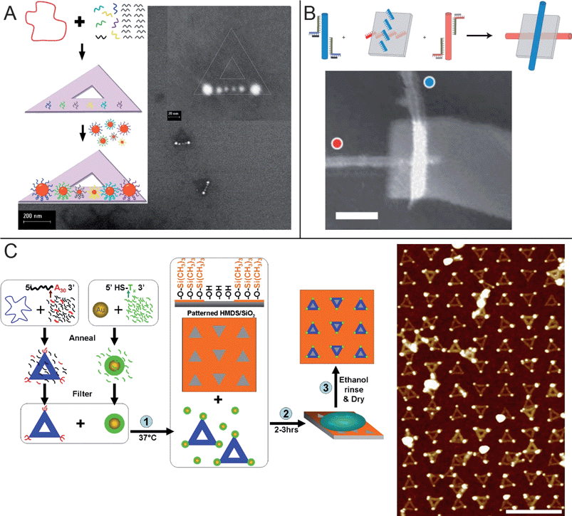 | ||
| Fig. 3 Examples of using DNA origami as templates for directed assembly of nanocomponents. (a) A self-similar chain of different sized gold nanoparticles with potential use as a plasmonic lens assembled on a triangular origami.78 (b) An assembled CNT cross-junction with potential use as a field-effect transistor.79 Scale bar, 50 nm. (c) Integration of top-down lithography and DNA assembly to create a large-area array of 5 nm gold nanoparticles.88 Triangular origami were decorated with nanoparticles and adsorbed to electron-beam patterned substrates with controlled placement and orientation. Scale bar: 500 nm. | ||
For origami to be used as templates to build devices, it is critical to deposit the DNA origami at prescribed locations with controlled orientation and at high yields. In one study, site-specific placement of rectangular origami was achieved by binding them to an array of similarly sized spots of gold functionalized with a carboxylic acid-terminated self-assembled monolayer (SAM).84 Divalent magnesium cations coordinate the negative charges of the SAM and those of the DNA, allowing non-covalent but selective adsorption of the DNA to the surface. With free 12-mer thymine strands extended from some of the staples, the origami also captured adenine-coated 10 nm gold nanoparticles from solution. Dielectrophoretic forces can also be used to trap origami on a surface between nanoelectrodes, and modifying the DNA structure with thiol groups allows for limited orientation determination via binding to the gold electrodes.85 As a means to get both positional and orientational control of origami placement, Kershner and coworkers recently showed that it was possible to selectively adsorb triangular DNA origami to etched features in two types of technologically relevant resists: diamond-like carbon (DLC) and a trimethyl silane (TMS) monolayer on silicon with native oxide.86 Electron-beam lithography was used to define 90 to 130 nm sized triangles with sharp corners which allowed for very good control over both placement and orientation of individual DNA origami. Adsorption of origami on DLC was mediated by a chemical difference between the etched and pristine surfaces of the resist, with the etched surface being hydrophilic and containing more oxygenated groups. In the case of the TMS monolayer, the hydrophobic groups were etched away within the features to expose clean native oxide, and adsorption was mediated by hydrophobic repulsion and electrostatic attraction to the oxide under high concentrations of divalent cations. For both DLC and TMS, quantitative adsorption of origami was observed at Mg2+ concentrations around 100 mM but almost no adsorption at concentrations an order of magnitude increased or decreased. This behavior is similar to what was observed for dsDNA on mica,87 and it is attributed to insufficient charge inversion of the negatively charged silanol surface at 10 mM Mg2+ and binding of excess Mg2+ to DNA (charge inversion or overcharging of the DNA) at 100 mM. Adjusting the ionic strength of the buffer in this manner may thus be used to tune the attractive force between the substrate and DNA, triggering adsorption or desorption.
Expanding on the work with TMS/oxide surfaces, Hung and coworkers recently described a complete process for directing the assembly of dry, large-scale, ordered arrays of gold nanoparticles on the patterned DNA origami, thereby demonstrating an unprecedented integration of top-down lithography with bottom-up self-assembly of sub-20 nm objects.88 DNA origami triangles were modified to bind ssDNA-coated 5 nm gold nanoparticles from solution, and the nanoparticle-decorated origami were adsorbed with controlled orientation and placement to e-beam patterned TMS/oxide substrates (Fig. 3c). In addition, an ethanol rinsing procedure was developed to remove excess buffer, salts, gold, and origami to yield a clean, dry array of DNA origami and nanoparticles. Optimization of factors such as gold concentration, origami concentration, and nanocrystal binding conditions was necessary to achieve high yields and clean arrays. Previous work had shown possible solutions to parts of the problem, but all of these disparate procedures were not guaranteed to be compatible with each other when put together. Importantly, the nanoparticles showed registry not only on each individual origami, but also to nanoparticles on the other origami and to the e-beam pattern as a whole.
Moving forward
Within the past five years, the most impressive advances in DNA-based assembly and fabrication have been the advent of a wide variety of synthetic DNA structures assembled from synthetic and genomic strands of DNA. The ability to rationally design biological structures from an almost infinite number of sequences makes DNA nanotechnology enormously flexible, and the imagination abounds with what other structures can possibly be made out of DNA. Can DNA tiles be assembled into patterns with low symmetry or purposeful directionality so as to be able to guide matter transport with reusable molecular motors or energy transport with electrically or optically active material components? Can DNA tiles be designed to assemble a 2D quasicrystal lattice of metal nanoparticles? In order for such DNA-based fabrication and devices to be viable however, the obstacles encountered in attempting to reliably find and address individual nanostructures need to be dealt with as well. While DNA tiles and origami have proven themselves very adept at creating high resolution patterns and using unique sequences to create multicomponent structures, there is significant room to develop more compelling methods to control their placement and orientation.The benefits of merging top-down lithography with biological self-assembled structures are obvious, but major hurdles remain. At the top-down end, each of the various lithographic techniques available have their own strengths and weaknesses. While contact-based printing approaches allow for facile patterning of biomolecules over large areas, they must be demonstrated to be robust (minimal degradation of the master pattern) over not 10 but 1,000 or 10,000 cycles. Scanning probe-based methods can offer superior resolution but need to become more like a parallel process, perhaps by using multiple probe arrays. Giving consideration to the specific problem at hand, integration of top-down and bottom-up processes, the most common role of the lithographic pattern is to provide localized, regular confinement, whether by affinity binding, topography, or applied forces. Thus, a more salient question may be how well can DNA be confined on a surface? The most interesting answers may well come from unique lithographic processes that combine multiple forms of confinement such as the surface tension forces and topographical patterns used to generate arrays of aligned λ-DNA.36
From the bottom-up, larger DNA structures may be able to interface more easily with lithographic patterns, but how large can one make a DNA origami or tile structure while maintaining decent yields and a unique sequence throughout? In general, all forms of self-assembly, from the assembly of the DNA scaffold to the binding of nanoscale components and the deposition of DNA scaffolds to patterned surfaces, will benefit from a better understanding of the underlying physical phenomena at work. For instance, the interplay between the length or sequence of a DNA linker attached to a gold nanocrystal, nanocrystal diffusion, and nanocrystal binding via DNA hybridization is not clear. Most likely, defects will need to be accepted as a given for any assembly-based process and compensated for by unique device designs or other means.
As work continues at the interface between the top-down and bottom-up regimes, specific problems regarding integration are coming into focus as well. One open question is how high is high enough for the resolution of the lithographic pattern. For example, positioning of individual origami only requires 100 nm features, but controlling the orientation requires higher resolutions to be able to register specific aspects of the origami shape such as sharp corners. Unique DNA origami designs or assembly methods may need to be developed to address this issue. Ensuring that each processing step is compatible with the others is another requirement that is often overlooked. Stability of the DNA structure, of the nanocomponent suspension, and of the bonds that hold everything together are typically the properties most sensitive to processing conditions such as ionic strength of the buffer solution. Many new challenges are also bound to arise as the field of DNA-based directed assembly progresses, but while the gap between top-down and bottom-up processes remains difficult to bridge, it is certainly getting smaller.
References
- C. M. Niemeyer and U. Simon, Eur. J. Inorg. Chem., 2005, 3641 CrossRef CAS.
- C. Lin, Y. Liu and H. Yan, Biochemistry, 2009, 48, 1663 CrossRef CAS.
- H. A. Becerril and A. T. Woolley, Chem. Soc. Rev., 2009, 38, 329 RSC.
- N. C. Seeman, Annu. Rev. Biochem., 2010, 79, 65 CrossRef CAS.
- N. C. Seeman, J. Theor. Biol., 1982, 99, 237 CrossRef CAS.
- J. Bath and A. J. Turberfield, Nat. Nanotechnol., 2007, 2, 275 CrossRef CAS.
- B. D. Gates, Q. B. Xu, M. Stewart, D. Ryan, C. G. Willson and G. M. Whitesides, Chem. Rev., 2005, 105, 1171 CrossRef CAS.
- A. Perl, D. N. Reinhoudt and J. Huskens, Adv. Mater., 2009, 21, 2257 CrossRef CAS.
- K. Salaita, Y. H. Wang and C. A. Mirkin, Nat. Nanotechnol., 2007, 2, 145 CrossRef CAS.
- M. J. Heller, Annu. Rev. Biomed. Eng., 2002, 4, 129 CrossRef CAS.
- I. Barbulovic-Nad, M. Lucente, Y. Sun, M. J. Zhang, A. R. Wheeler and M. Bussmann, Crit. Rev. Biotechnol., 2006, 26, 237 CrossRef CAS.
- B. Kannan, R. P. Kulkarni and A. Majumdar, Nano Lett., 2004, 4, 1521 CrossRef CAS.
- L. M. Demers, D. S. Ginger, S. J. Park, Z. Li, S. W. Chung and C. A. Mirkin, Science, 2002, 296, 1836 CrossRef CAS.
- M. Z. Liu, N. A. Amro, C. S. Chow and G. Y. Liu, Nano Lett., 2002, 2, 863 CrossRef CAS.
- S. Sun, D. Thompson, U. Schmidt, D. Graham and G. J. Leggett, Chem. Commun., 2010, 46, 5292 RSC.
- J. U. Park, J. H. Lee, U. Paik, Y. Lu and J. A. Rogers, Nano Lett., 2008, 8, 4210 CrossRef CAS.
- Y. N. Xia and G. M. Whitesides, Annu. Rev. Mater. Sci., 1998, 28, 153 CrossRef CAS.
- S. A. Lange, V. Benes, D. P. Kern, J. K. H. Horber and A. Bernard, Anal. Chem., 2004, 76, 1641 CrossRef CAS.
- M. H. S. Shyr, D. P. Wernette, P. Wiltzius, Y. Lu and P. V. Braun, J. Am. Chem. Soc., 2008, 130, 8234 CrossRef CAS.
- W. L. Cheng, N. Y. Park, M. T. Walter, M. R. Hartman and D. Luo, Nat. Nanotechnol., 2008, 3, 682 CrossRef CAS.
- M. M. Maye, M. T. Kumara, D. Nykypanchuk, W. B. Sherman and O. Gang, Nat. Nanotechnol., 2010, 5, 116 CrossRef CAS.
- M. E. Leunissen, R. Dreyfus, F. C. Cheong, D. G. Grier, R. Sha, N. C. Seeman and P. M. Chaikin, Nat. Mater., 2009, 8, 590 CrossRef CAS.
- W. A. Zhao, W. Chiuman, J. C. F. Lam, S. A. McManus, W. Chen, Y. G. Cui, R. Pelton, M. A. Brook and Y. F. Li, J. Am. Chem. Soc., 2008, 130, 3610 CrossRef CAS.
- A. J. Kim, R. Scarlett, P. L. Biancaniello, T. Sinno and J. C. Crocker, Nat. Mater., 2009, 8, 52 CrossRef CAS.
- M. Geissler, E. Roy, J. S. Deneault, M. Arbour, G. A. Diaz-Quijada, A. Nantel and T. Veres, Small, 2009, 5, 2514 CrossRef CAS.
- S. R. Coyer, A. J. Garcia and E. Delamarche, Angew. Chem., Int. Ed., 2007, 46, 6837 CrossRef CAS.
- H. Noh, A. M. Hung, C. Choi, J. H. Lee, J. Y. Kim, S. Jin and J. N. Cha, ACS Nano, 2009, 3, 2376 CrossRef CAS.
- I. Y. Wong and N. A. Melosh, Nano Lett., 2009, 9, 3521 CrossRef CAS.
- A. Bernard, D. Fitzli, P. Sonderegger, E. Delamarche, B. Michel, H. R. Bosshard and H. Biebuyck, Nat. Biotechnol., 2001, 19, 866 CrossRef CAS.
- O. Akbulut, A. A. Yu and F. Stellacci, Chem. Soc. Rev., 2010, 39, 30 RSC.
- A. A. Yu, T. A. Savas, G. S. Taylor, A. Guiseppe-Elie, H. I. Smith and F. Stellacci, Nano Lett., 2005, 5, 1061 CrossRef CAS.
- J. Kim and R. M. Crooks, J. Am. Chem. Soc., 2006, 128, 12076 CrossRef CAS.
- Y. D. Wang, S. H. Goh, X. Y. Bi and K. L. Yang, J. Colloid Interface Sci., 2009, 333, 188 CrossRef CAS.
- O. Akbulut, J. M. Jung, R. D. Bennett, Y. Hu, H. T. Jung, R. E. Cohen, A. M. Mayes and F. Stellacci, Nano Lett., 2007, 7, 3493 CrossRef CAS.
- Q. Gu, C. D. Cheng, R. Gonela, S. Suryanarayanan, S. Anabathula, K. Dai and D. T. Haynie, Nanotechnology, 2006, 17, R14 CrossRef CAS.
- J. J. Guan and J. Lee, Proc. Natl. Acad. Sci. U. S. A., 2005, 102, 18321 CrossRef CAS.
- H. J. Xin and A. T. Woolley, Nanotechnology, 2005, 16, 2238 CrossRef CAS.
- H. Nakao, Anal. Sci., 2009, 25, 1387 CrossRef CAS.
- K. Keren, R. S. Berman, E. Buchstab, U. Sivan and E. Braun, Science, 2003, 302, 1380 CrossRef CAS.
- G. A. Burley, J. Gierlich, M. R. Mofid, H. Nir, S. Tal, Y. Eichen and T. Carell, J. Am. Chem. Soc., 2006, 128, 1398 CrossRef CAS.
- A. P. Alivisatos, K. P. Johnsson, X. G. Peng, T. E. Wilson, C. J. Loweth, M. P. Bruchez and P. G. Schultz, Nature, 1996, 382, 609 CrossRef CAS.
- S. Shukla and M. Sastry, Nanoscale, 2009, 1, 122 RSC.
- K. Tanaka, G. H. Clever, Y. Takezawa, Y. Yamada, C. Kaul, M. Shionoya and T. Carell, Nat. Nanotechnol., 2006, 1, 190 CrossRef CAS.
- H. Yang, C. K. McLaughlin, F. A. Aldaye, G. D. Hamblin, A. Z. Rys, I. Rouiller and H. F. Sleiman, Nat. Chem., 2009, 1, 390 Search PubMed.
- J. D. Le, Y. Pinto, N. C. Seeman, K. Musier-Forsyth, T. A. Taton and R. A. Kiehl, Nano Lett., 2004, 4, 2343 CrossRef CAS.
- J. P. Zhang, Y. Liu, Y. G. Ke and H. Yan, Nano Lett., 2006, 6, 248 CrossRef CAS.
- J. Sharma, R. Chhabra, Y. Liu, Y. G. Ke and H. Yan, Angew. Chem., Int. Ed., 2006, 45, 730 CrossRef CAS.
- J. W. Zheng, P. E. Constantinou, C. Micheel, A. P. Alivisatos, R. A. Kiehl and N. C. Seeman, Nano Lett., 2006, 6, 1502 CrossRef CAS.
- S. Pal, Z. T. Deng, B. Q. Ding, H. Yan and Y. Liu, Angew. Chem. Int. Ed., 2010, 49, 2700 CAS.
- J. Sharma, R. Chhabra, C. S. Andersen, K. V. Gothelf, H. Yan and Y. Liu, J. Am. Chem. Soc., 2008, 130, 7820 CrossRef CAS.
- J. Sharma, Y. G. Ke, C. X. Lin, R. Chhabra, Q. B. Wang, J. Nangreave, Y. Liu and H. Yan, Angew. Chem., Int. Ed., 2008, 47, 5157 CrossRef CAS.
- S. H. Park, P. Yin, Y. Liu, J. H. Reif, T. H. LaBean and H. Yan, Nano Lett., 2005, 5, 729 CrossRef CAS.
- A. Kuzuya, M. Kimura, K. Numajiri, N. Koshi, T. Ohnishi, F. Okada and M. Komiyama, ChemBioChem, 2009, 10, 1811 CrossRef CAS.
- R. Chhabra, J. Sharma, Y. G. Ke, Y. Liu, S. Rinker, S. Lindsay and H. Yan, J. Am. Chem. Soc., 2007, 129, 10304 CrossRef CAS.
- Y. He, Y. Tian, A. E. Ribbe and C. D. Mao, J. Am. Chem. Soc., 2006, 128, 12664 CrossRef CAS.
- B. A. R. Williams, K. Lund, Y. Liu, H. Yan and J. C. Chaput, Angew. Chem., Int. Ed., 2007, 46, 3051 CrossRef CAS.
- C. Song, Y. Q. Chen, S. J. Xiao, L. Ba, Z. Z. Gu, Y. Pan and X. Z. You, Chem. Mater., 2005, 17, 6521 CrossRef CAS.
- J. Sharma, R. Chhabra, A. Cheng, J. Brownell, Y. Liu and H. Yan, Science, 2009, 323, 112 CrossRef CAS.
- J. Malo, J. C. Mitchell, C. Venien-Bryan, J. R. Harris, H. Wille, D. J. Sherratt and A. J. Turberfield, Angew. Chem., Int. Ed., 2005, 44, 3057 CrossRef CAS.
- H. Yan, S. H. Park, G. Finkelstein, J. H. Reif and T. H. LaBean, Science, 2003, 301, 1882 CrossRef CAS.
- D. Liu, S. H. Park, J. H. Reif and T. H. LaBean, Proc. Natl. Acad. Sci. U. S. A., 2004, 101, 717 CrossRef CAS.
- Y. Liu, C. X. Lin, H. Y. Li and H. Yan, Angew. Chem., Int. Ed., 2005, 44, 4333 CrossRef CAS.
- Y. Weizmann, A. B. Braunschweig, O. I. Wilner, Z. Cheglakov and I. Willner, Proc. Natl. Acad. Sci. U. S. A., 2008, 105, 5289 CrossRef CAS.
- P. K. Lo, P. Karam, F. A. Aldaye, C. K. McLaughlin, G. D. Hamblin, G. Cosa and H. F. Sleiman, Nat. Chem., 2010, 2, 319 Search PubMed.
- R. Schulman and E. Winfree, Proc. Natl. Acad. Sci. U. S. A., 2007, 104, 15236 CrossRef CAS.
- O. I. Wilner, Y. Weizmann, R. Gill, O. Lioubashevski, R. Freeman and I. Willner, Nat. Nanotechnol., 2009, 4, 249 CrossRef CAS.
- S. H. Park, C. Pistol, S. J. Ahn, J. H. Reif, A. R. Lebeck, C. Dwyer and T. H. LaBean, Angew. Chem., Int. Ed., 2006, 45, 735 CrossRef CAS.
- F. A. Aldaye and H. F. Sleiman, J. Am. Chem. Soc., 2007, 129, 4130 CrossRef CAS.
- P. W. K. Rothemund, N. Papadakis and E. Winfree, PLoS Biol., 2004, 2, e424 CrossRef.
- K. Fujibayashi, R. Hariadi, S. H. Park, E. Winfree and S. Murata, Nano Lett., 2008, 8, 1791 CrossRef CAS.
- R. D. Barish, R. Schulman, P. W. K. Rothemund and E. Winfree, Proc. Natl. Acad. Sci. U. S. A., 2009, 106, 6054 CrossRef CAS.
- K. Sarveswaran, W. C. Hu, P. W. Huber, G. H. Bernstein and M. Lieberman, Langmuir, 2006, 22, 11279 CrossRef CAS.
- C. X. Lin, Y. G. Ke, Y. Liu, M. Mertig, J. Gu and H. Yan, Angew. Chem., Int. Ed., 2007, 46, 6089 CrossRef CAS.
- A. Kuzuya and M. Komiyama, Nanoscale, 2010, 2, 310 RSC.
- P. W. K. Rothemund, Nature, 2006, 440, 297 CrossRef CAS.
- Y. G. Ke, S. Lindsay, Y. Chang, Y. Liu and H. Yan, Science, 2008, 319, 180 CrossRef CAS.
- S. Rinker, Y. G. Ke, Y. Liu, R. Chhabra and H. Yan, Nat. Nanotechnol., 2008, 3, 418 CrossRef CAS.
- B. Q. Ding, Z. T. Deng, H. Yan, S. Cabrini, R. N. Zuckermann and J. Bokor, J. Am. Chem. Soc., 2010, 132, 3248 CrossRef CAS.
- H. T. Maune, S. P. Han, R. D. Barish, M. Bockrath, W. A. Goddard, P. W. K. Rothemund and E. Winfree, Nat. Nanotechnol., 2010, 5, 61 CrossRef CAS.
- K. Lund, A. J. Manzo, N. Dabby, N. Michelotti, A. Johnson-Buck, J. Nangreave, S. Taylor, R. J. Pei, M. N. Stojanovic, N. G. Walter, E. Winfree and H. Yan, Nature, 2010, 465, 206 CrossRef CAS.
- H. Z. Gu, J. Chao, S. J. Xiao and N. C. Seeman, Nat. Nanotechnol., 2009, 4, 245 CrossRef CAS.
- H. Z. Gu, J. Chao, S. J. Xiao and N. C. Seeman, Nature, 2010, 465, 202 CrossRef CAS.
- N. V. Voigt, T. Torring, A. Rotaru, M. F. Jacobsen, J. B. Ravnsbaek, R. Subramani, W. Mamdouh, J. Kjems, A. Mokhir, F. Besenbacher and K. V. Gothelf, Nat. Nanotechnol., 2010, 5, 200 CrossRef CAS.
- A. E. Gerdon, S. S. Oh, K. Hsieh, Y. Ke, H. Yan and H. T. Soh, Small, 2009, 5, 1942 CrossRef CAS.
- A. Kuzyk, B. Yurke, J. J. Toppari, V. Linko and P. Törmä, Small, 2008, 4, 447 CrossRef CAS.
- R. J. Kershner, L. D. Bozano, C. M. Micheel, A. M. Hung, A. R. Fornof, J. N. Cha, C. T. Rettner, M. Bersani, J. Frommer, P. W. K. Rothemund and G. M. Wallraff, Nat. Nanotechnol., 2009, 4, 557 CrossRef CAS.
- D. Pastré, L. Hamon, F. Landousy, I. Sorel, M. O. David, A. Zozime, E. Le Cam and O. Piétrement, Langmuir, 2006, 22, 6651 CrossRef CAS.
- A. M. Hung, C. M. Micheel, L. D. Bozano, L. W. Osterbur, G. M. Wallraff and J. N. Cha, Nat. Nanotechnol., 2010, 5, 121 CrossRef CAS.
| This journal is © The Royal Society of Chemistry 2010 |