DOI:
10.1039/C0NR00352B
(Review Article)
Nanoscale, 2010,
2, 2521-2529
The creation of nanojunctions
Received
29th May 2010
, Accepted 21st July 2010
First published on
17th September 2010
Abstract
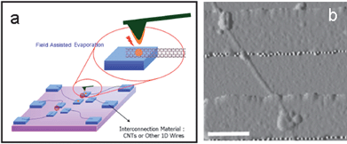
This review describes recent progress in creation of nanojunctions between individual nanoobjects. The accomplishments of various strategies used for nanojunction creation are highlighted and the corresponding challenges are discussed. The possible ongoing development for the creation of device-oriented nanojunctions is speculated upon.
 Shouwu Guo | Shouwu Guo received his PhD degree from the Weizmann Institute of Science, Israel, in 1999. From 1999 to 2005, he worked as a postdoctoral and research scientist in University of Minnesota and Northwestern University, USA. He joined the Research Institute of Micro/Nano Science and Technology at Shanghai Jiao Tong University at the end of 2005 as a professor. His research interests are focused on synthesis of nanosized materials, controllable nanofabrication and nanomanipulation based on scanning probe microscopy and application of nanostructured materials in biocatalysts and sensors. |
1. Introduction
Nanoobjects, such as nanospheres, nanowires, nanodisks, and nanotetrapods, have attracted substantial attention during last two decades, due to their unique properties and potential applications in many areas.1–3 The well established methodologies for control over the composition, size, and morphology of the nanosized materials made it possible to fabricate nanoobjects with desired functionality and geometry for device applications.4,5 So far, several prototype nanodevices consisting of a single nanoobject, such as molecule sensors,6–8 field-effect transistors,9–11 and single-electron transistors12 have been reported. However, it is still challenging to connect a single nanoobject to a micro/macro object, such as an electrode, with a stable Ohmic contact, which is a key issue for nanoelectronic device manufacturing. In comparison to single nanoobject based devices, nanodevices consisting of several individual nanoobjects should have more functionalities, broadening their applicability.13,14 However, the assembly of several individual nanoobjects into a multiterminal device will encounter even more technical challenges. Besides making a stable contact between a nanoobject and micro/macro object, as aforementioned for a single nanoobject based device, for multiterminal nanodevice construction, the critical technical challenges are to manipulate nanoobjects, including moving or placing an individual nanoobject to the desired sites on a solid substrate, and then interconnecting them with robust nanojunctions.
The manipulation of a single nanoobject, such as moving and placing of nanoparticles on a bulk substrate surface, has been realized using scanning probe microscope,15,16 electron microscope,17,18 or nanorobotic manipulator,19 though these approaches are still time consuming. To join the nanoobjects together, a range of methods has also been developed. In general, there are three different methods can be followed. One is to place the nanoobjects, such as nanotubes or nanowires, to cross over each other, forming physical contacts. Due to their poor mechanical properties and high contact electrical resistance, nanoobjects joined through physical contact might be only applicable for Schottky devices, but not for others.12 The second method is to grow the branched nanostructure directly. By controlling the synthetic experimental conditions, a range of the branched nanostructures have already been generated, in which the branches are joined together with a common center, forming nanojunctions. The third way is to create a nanojunction between the individual nanoobjects ex situ. For example, using electron-beam irradiation techniques, nanojunctions were generated between carbon nanotubes, and other one-dimensional nanostructures. Other methods, including thermal and electrical welding, lasers and Joule heating have also been employed for creating nanojunctions. Recently, atomic force microscopy (AFM) based combined-dynamic-mode dip-pen nanolithography (CDDPN) technique was utilized for generation of the nanojunctions between/among carbon nonotubes and showed good site-specific and environmentally friendly advantages. The mechanical properties and functionalities of as-generated nanojunctions by CDDPN could be easily tuned by choosing appropriate precursor materials for the nanojunctions. Thus, with further improvement, the nanoobjects interconnected through stable nanojunctions created with AFM based nanolithography may find practical applications in a diversity of switching, logic, transistor, and computing devices.20
In this review, we will mainly focus on the methodologies that have been developed to create nanojunctions. For the sake of clarity, the performances of the nanojunctions in nanodevices are not covered herein. First, we will discuss the direct growth of the branched nanostructures containing homo-nanojunctions. The properties of the branched nanostrucures will be briefly discussed as well. Second, we will present mainly the creation of nanojunctions between individual nanoobjects based on electron beam irradiation. Third, the formation of nanojunctions in high electric, thermal (Joule heating), and optical (laser) fields will be reviewed. Finally, we will describe the nondestructive creation of nanojunctions using AFM based nanofabication techniques.
During last two decades, various branched nanostructures have been prepared using the direct growth method. In a branched nanostructure, the branches, such as nanowires and nanotubes, are joined together with a common center forming stable nanojunctions. Nanojunction centers generated through the direct growth method usually have the same composition and structure within the branches.21 Chemical vapor deposition (CVD) with/without the catalysts, high temperature gas/solid reaction, and simple solution based chemical reactions have been utilized for the direct growth of branched nanostructures. In 1998, following a variety of computation-based theoretical studies on the nanojunctions formed between carbon nanotubes (CNT) with different properties (metallic or semiconducting) and radii,22,23 Han et al. prepared single-wall carbon nanotube (SWNT) bends with the bending angles from 18° to 34° using the catalytic decomposition of hydrocarbons (Fig. 1). Based on molecular dynamics (MD) simulation, the bends were believed to be the two-terminal nanojunctions formed between SWNTs through topological defects (i.e., pentagon–heptagon pairs).24 Soon after that, branched multiwalled carbon nanotubes (MWNT) were successfully produced using a template-assistant CVD procedure by Li and Papadopoulos et al., in which three terminal nanojunctions, namely Y-type nanojunctions, were recognized (Fig. 2).25 The as-generated Y-type nanojunctions showed nonlinear electron transport and rectifying behaviors at room temperature.25,26 Using a simple pyrolysis of nickelocene and thiophene at 1000 °C, Satishkumar et al. prepared branched MWNTs containing Y-type nanojunctions, too (Fig. 3). They found also the I–V characteristics at the Y junction are asymmetric with respect to zero bias as in a junction diode.27 Following those pioneering works, branched MWNTs with similar Y-type nanojunctions were generated through many other procedures.28–31
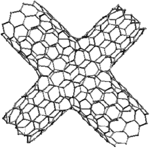
In contrast to the aforementioned nanojunctions consisting of carbon nanotubes with the same tube diameter and wall thickness, Jin et al. developed a facile two-step CVD strategy, using Fe/Mo nanopartciles as catalysts and C2H2/CH4 as carbon source, and produced a serial nanojunctions between carbon nanotubes with different wall structures and diameters (Fig. 4).32 Computational simulation studies have predicted that multiterminal nanojunctions, such as X-type nanojunctions (Fig. 5) of carbon nanotubes should have more functionality, and might find more practical applications in nanodevices, such as nanocircuits and nanosystems.21 However, the direct synthesis of such kind of multiterminal nanojunctions has been barely reported. Wang et al. observed that several CNTs crossed over each other when a bulk aluminium substrate was used as a catalyst for CNT growth, but the formation of fastenened (stable) multiterminal nanojunctions remained to be debated.33 Indeed, the multiterminal nanojunctions of CNTs could be rationally designed and fabricated using nanowelding and nanosoldering techniques based on electron beam irradiation or other methods, which will be reviewed in detail in the following sections.
 |
| | Fig. 5 X-Type nanojunction of SWNT as predicted by computational simulations.21 | |
Carbon nanotubes show either metallic or semiconducting properties depending on their diameter and chirality.34–36 In contrast, boron nitride (BN) nanotubes are wide band gap semiconductors, and have a high resistance to oxidation at high temperature, excellent thermal conductivity, and strong mechanical properties.37,38 Thus, BN nanotubes have been considered as another useful one-dimensional nanoobject for nanodevices. However, to assemble BN nanotubes/nanowires into nanodevices, the creation of nanojunctions between individual BN nanotubes/nanowires should be an important issue, too. Cao et al. developed a simple approach for the large scale synthesis of branched BN nanotubes having uniform Y-type nanojunctions by annealing branched boron nanowire precursors in N2 atmosphere at 1500 °C (Fig. 6). The conversion of solid boron nanowire to a tubular BN structure was attained through several steps, including the reaction of nitrogen with boron at the nanowire surface, interdiffusion of boron atoms, and the migration and rearrangement of BN.36,39 This method opened a novel route to generating a diversity of nanojunctions between tubular nanoobjects.
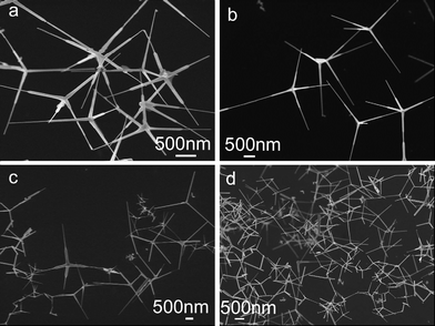
Zinc oxide (ZnO), a well-known semiconductor, holds great promise for many applications in field emission devices, piezoelectric devices, solar cells, and lasers due to its wide direct band gap (3.37 eV) and large exciton binding energy (∼60 meV). Besides the nanoparticles, nanowires (nanorods), and nanoribbons have been synthesized that prompted much more research on their unique structural character and potential applications.40–45 More recently, Zhang et al. synthesized tetrapod-like ZnO nanostructures with uniform hexagonal prism legs simply through oxidization of zinc vapor followed by ZnO condensation at relatively lower temperatures. As shown in Fig. 7, the common structural feature of the tetrapod ZnO nanostructures is that the four tetrahedrally arranged legs are connected at a common center forming stable nanojunctions.44,45 The researches on tetrapod ZnO nanocrystals have been nicely reviewed, and the reader is referred to ref. 46 for comprehensive examinations.46
 |
| | Fig. 7 SEM images of tetrapod ZnO nanocrystals synthesized under a zinc oxidation time of 30 min, a ZnO condensation temperature of 500 °C, and a ZnO condensation time of 0 (a), 20 (b), 90 (c), and 120 min (d).45 | |
As aforementioned, through direct growth, many kinds of nanojunctions could be obtained. The nanojunctions sometimes showed unique properties differing from those of the individual nanoparticles, and may have potential applications in nanodevice construction. However, for the nanojunctions that were formed through chemical reactions including the CVD, a big drawback is the lack of the control of the type, size, and the specific location of the nanojunctions. This severely limits the applications of the branched nanostructures in nanodevices. In addition, the problem of the connections between branched nanostructures and micro/macroobjects remains to be solved.
3. Creation of nanojunctions via electron beam irradiation
Transmission electron microscopy (TEM) and scanning electron microscopy (SEM) usually are employed to characterize the structures of nanosized materials.47–50 With a modern field emission TEM and SEM, the electron beam spot can be focused on a spot of less than 1 nm in diameter, the electrons can be accelerated to hundreds of keV with the highest possible electron beam intensity of 106 A cm−2.51,52 The high energy electrons could interact with the specimen surfaces both elastically and inelastically, inducing sputtering,53 desorption,54 phase-transition,55 and so on.51 Thus, several nanofabrication techniques, most pronouncedly electron beam lithography,56 have been developed.
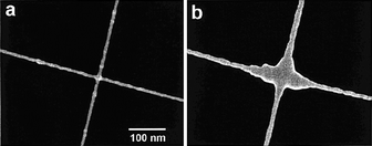
More recently, with the high intensity electron beam, a range of nanojunctions have been generated between individual nanoobjects. Banhart57 reported that hydrocarbon molecules (as contaminants from environments that include the oil-pumping system of TEM) attracted at the crossing site of two MWNTs could be transformed into amorphous carbon, forming a nanojunction at the crossing site of the two MWNTs under high energy electron beam irradiation, as shown in Fig. 8. The TEM study illustrated that after annealing with further high energy electron beam irradiation, the amorphous carbon nanojunctions underwent graphitization. Instead of the use of trace hydrocarbon molecules attracted to the surfaces of MWNTs, organometallic compounds can be vaporized into different species when they are heated by an electron beam. The vaporized species could be adsorbed on the surface of the nanoobjects in the electron microscopy chamber, and are then decomposed under additional high energy electron beam irradiation. Using this procedure, Gopal et al. fabricated the metal (Pt and Ag) nanojunctions and nanocontacts in prototypical circuits incorporating carbon nanotubes.58 More particularly, based on piezodriven nanomanipulation and the electron beam induced deposition of amorphous carbon, a variety of CNT nanojunctions, including end-to-end, side-to-side, zig-zag, and networks, have been produced systematically (Fig. 9), and their electrical and mechanical properties have also been measured in situ with the TEM revealing that the carbon nanotubes were readily joined together with moderate junction resistance and excellent mechanical strength.59,60
 |
| | Fig. 8 Scanning electron microscopy images of a nanotube junction before (a) and after (b) soldering by deposition of amorphous carbon. Due to a high contamination rate, the deposit at the junction is large. Some contamination is already visible in (a) due to inevitable irradiation during recording of the SEM image (droplets on the tubes).57 | |
 |
| | Fig. 9 TEM images showing the different nanojunctions generated between carbon nanotubes. (a) end-to-end, (b) side-to-side, (c) zig-zag, and (d) network nanojunctions. The nanojunction centers were composed of amorphous carbon.59 | |
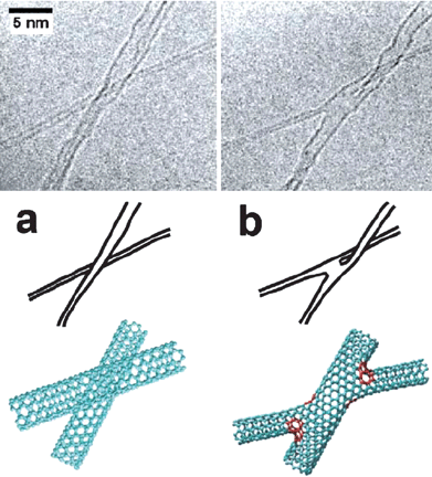
Alternatively, without using any hydrocarbon contaminants or precursors, Terrones et al. found that by the exposure of the crossed SWNTs to an electron beam in a TEM chamber, molecular junctions could be generated at the crossing sites of the SWNTs, as shown in Fig. 10.61 The formation of molecular junction should originate from the cross-linking between dangling bonds that are generated by high energy electron beam irradiation at high temperature. Following this strategy, several different kinds of CNT nanojunctions were created.61
 |
| | Fig. 10 (a) A SWNT of ca. 2.0 nm in diameter (running from the bottom-left diagonally towards the top right) crossing with an individual SWNT of ca. 0.9 nm in diameter. (b) 60 s of electron irradiation promotes a molecular connection between the thin and the wide tube, forming an “X” junction. Schematics show that this junction is twisted out of the plane. Molecular models of each image are provided; heptagonal rings are indicated in red.61 | |
Combining the SEM and a piezodriven nanomanipulator, individual MWNTs were mounted on tungsten support tips forming carbon–tungsten hetero nanojunctions.62 More diversely, Xu et al. illustrated that the focused high-intensity-electron beam could melt the metal nanowire locally, which enables the welding together of Au, Ag, Cu, Ni, Sn and Si nanowires in a controlled way to form rationally designed nanojunctions.51Fig. 11 shows Au nanowires being joined together by focused high-intensity-electron beam irradiation at the crossing sites of Au nanowires forming a closed loop. The nanojunction joint loop was then cut off from the rest of the nanowires using further focused high-intensity electron beam irradiation.51 The hetero-nanojunctions were also prepared using metal filled MWNTs as precursors under intense electron beam irradiation at temperatures of 450 to 700 °C depending on the filling metals.63 Under irradiation at high temperature, the segregation of metal and carbon atoms occurs, resulting in the formation of hetero-nanojunctions between metal and graphite (Fig. 12). It was found also that as-generated nanojunctions through this method preserved their metallic conductivity. The density functional calculations show that these nanojunctions are mechanically strong, the bonding at the interface is covalent, and the electronic states at and around the Fermi level are delocalized across the entire system. These properties are essential for the application of such hetero-nanojunctions in electronic devices.63
 |
| | Fig. 11 Welding of three single-crystalline Au NWs with a 10-nm diameter HIEB. (a) The original Au NWs. (b–d) A closed loop is formed after welding the NWs together at their overlapping regions (highlighted by arrows), and then the loop is cut off from the rest of the NWs. Holes are seen in the supporting carbon film under the joints. The whole process from (a) to (d) takes 30 min.51 | |
 |
| | Fig. 12 Formation of a MWNT–Co–MWNT junction from a Co-filled MWNT subjected to electron beam irradiation (200 keV) at 700 °C. (A) The Co-filled MWNT at the beginning of the experiment. (B) The focused electron beam damages the tube, and the Co nanowire is expelled to the surface, experiencing shape changes after 6 min of irradiation. (C) Finally, the Co particle acts as a link between the 2 MWNT segments. The time required to obtain the final shape was 11 min. The sketch at the bottom shows the mechanism of the process. The circle indicates the zone subjected to electron irradiation.63 | |
4. Nanojunctions formed in the high electric, optical and thermal fields
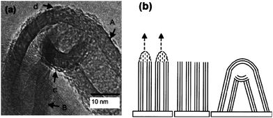
As mentioned above, under high energy electron beam irradiation, multiterminal nanojunctions, such as X-type, zig-zags, and closed loops, have been generated. In principle, the high electric, optical and thermal fields can also facilitate the formation of nanojunctions between nanoobjects. For instance, Ho et al. reported that the nanojunctions could be formed between MWNTs after application of a high electric field on an array of well-aligned MWNTs.64 When the field emission measurement was performed on an array of well-aligned multiwalled carbon nanotubes under vacuum (10−2 Torr) with a constant bias of 2000 V, after 8 h exposure to the electric field, the maximum emission current density of the multiwalled carbon nanotubes array dropped by 93%, and meanwhile the TEM image showed the formation of nanojunctions between carbon nanotubes (Fig. 13a). The mechanism of nanojunction formation was believed to be that, under a long time exposure to a high electric field, the electric field at the nanotube tips was large enough to break C–C bonds, causing C atom sublimation. The sublimated C atoms are likely to redeposit on the cooler tube walls, eventually leading to the formation of nanojunctions (Fig. 13b).64
 |
| | Fig. 13 (a) TEM image of a typical nanojunction formed by fusion of two adjacent tips under high electric field conditions. (b) Model illustrating formation of nanojunction structure in (a): (i) electric field as well as thermal effects lead to C–C bond breaking; (ii) nanotubes are left with open tips and structural defects; (iii) fusion of adjacent CNTs to form a nanojunction. The outer walls form a fairly continuous junction as seen at region d in (a). For the inner walls at region c, discontinuous and defective joints appear to have formed so as to minimize the energy that would have been required to form a high-curvature and high-stress junction.64 | |
When a constant direct current is applied to a conducting nanowire, large current induced heating, namely Joule heating, can be generated, which may introduce the local melting and/or the surface atoms migration leading to the formation of the nanojunctions.65,66 Using this technique, Tohmyoh et al. successfully welded two Pt nanowires together (Fig.14). They found that, due to atom migration, the Pt nanowires, at the same time, could be cut at certain sites by supplying a high current.65 The Joule heating was used to direct electron-beam-induced deposition of carbon on carbon nanotube surfaces, which was also used to prepare nanojunctions.67 Additionally, Joule heating could melt the nanocrystals encapsulated within the carbon nanotubes to achieve nano-robotic spot welding, thus, the nanojunctions could be generated in a more controllable manner.68 However, it has been demonstrated that during the current flow, Joule heating and electromigration cause the diffusion of atoms along the length of nanowires, and the failure of nanowires happened occasionally.65,69 Considering those problems, Peng et al. developed a novel nanosoldering technique to join the individual metallic nanoobjects using a nanoscale Sn solder. The nanoscale Sn solder (actually, a short Sn nanoweire) was placed precisely at the desired location using a nanomanipulator first installed in an SEM. Then, to avoid significant diffusion of the atoms along the nanowires caused with direct Joule heating, the Joule heating was introduced controllably just onto the nanoscale Sn solder to melt it, that generated finally a mechanically strong and electrically conductive nanocontact (nanojunctions).70
Each metal nanoparticle usually possesses a typical optical absorption band, and the nanoparticle can be heated above the melting point into a liquid-like nanoparticle under irradiation of the high power laser whose energy coincides with the absorption band,71 thus the laser-assisted heating of metal nanoparticles may result in nanojunction formation between them. Indeed, Ohmic-contact nanojunctions between platinum and gold nanoparticles were created in an aqueous dispersion under irradiation at the second harmonic (532 nm, which is close to the wavelength of the surface plasmon resonance absorption peak of gold nanoparticles) of a Nd:YAG pulsed laser.72 Similarly, Kim et al., using a picosecond pulsed laser, welded successfully two gold nanoparticles together as shown in Fig. 15.73
 |
| | Fig. 15 HRTEM images of gold nanoparticles held together and nanowelded by irradiating laser pulses of 532 nm and 0.2 mJ for 10 min on a carboncoated copper TEM grid, indicating that gold nanoparticles are welded in a single phase with an Ohmic nanocontact.73 | |
Using combined-dynamic-mode dip-pen nanolithography (CDDPN) technique based on AFM,79,80 Shen et al. developed a facile strategy for creating the nanojunctions between CNTs, and the procedure is schematically depicted in Fig. 17.81 Using Tollens' reagent and HAuCl4 aqueous solution as precursors, Ag and Au nanojunctions were created between SWNTs (Fig. 18). By dynamically exchanging the AFM operation between tapping and lifting modes during the CDDPN procedure, the site of the nanojunctions could be located specifically as desired; the size of the nanojunctions could be easily tuned.
 |
| | Fig. 17 Schematic representation of the procedure for creation of a nanojunction at a nanogap using combined-dynamic mode dip-pen nanolithography (CDDPN).81 | |
 |
| | Fig. 18 (a) Tapping mode AFM image of SWNTs crossed at sites 1, 2, 3 and 4 on hexamethyldisilazane modified silicon substrate. (b) Tapping mode AFM images of Ag nanojunctions with sizes of ∼161, ∼93, ∼68, and ∼59 nm in diameter created at the cross sites of 1, 2, 3 and 4. The contact times of the AFM tip with the substrate at the cross sites of 1, 2, 3 and 4 under the combined mode were 80, 50, 32 and 16 s, respectively.81 | |
6. Summary and outlook
The creation of nanojunctions between individual nanoobjects is of important for fabrication of multiterminal nanodevices. This review covered several recent methodological advances in creation of nanojunctions between individual nanoobjects, including direct growth of branched nanostructures, high energy electron beam irradiation, AFM based nanofabrication techniques, and high electric, optical, and thermal field enhanced nanofabrications. The direct growth of the branched nanostructure opened a facile route to preparation nanojunction, and can provide with a lots of nanojunctions with different morphologies. However, with direct growth, the nanojunctions were formed during the chemical reactions, and the morphology and dimension of the nanojunctions were unpredictable and thus poorly controlled, which limits it as a general preparation method for device-oriented nanojunctions. With the high energy electron beam irradiation technique, the nanojunctions could be generated in a more rational way, and the position and morphology of the nanojunctions could be easily controlled, but high energy electron beam irradiation, sometimes damages or contaminates the nanoobjects, which may in due course affect the properties of the nanoobjects. High electric and optical field (laser irradiation) have proven to be useful for creation of nanojunctions, but their poor spatial resolution needs to be improved further for use in real device fabrication. Joule heating has showed great promise, however, the morphology change of the nanoobjects caused by electromigration during the electric current flow remains unsolved. Atomic force microscopy based nanofabrication techniques, especially DPN and CDDPN, may provide a platform to generate nanojunctions in a more controllable way, but their low throughput is a big drawback.
Several methodologies have proven to be efficient in nanojunction creation between individual nanoobjects, but to achieve device-oriented nanojunctions, there is a lot of ongoing work that still needs to be done: (1) creation of a nanojunction specifically at the site according to the device design; (2) precise control of the morphology and dimension of the nanojunction; (3) control of the chemical composition and structure of nanojunctions. Ideally, the creation of homojunctions (with the same chemical composition and structure as the nanoobjects that are to be interconnected) which can avoid the undesirable interface effects caused by heterojunctions should be most important for real nanodevice applications.
Acknowledgements
This work was supported by the national “863 program” (No. 2006AA04Z309), the national “973 program” (Nos. 2007CB936000 and 2010CB933900), and the NSFC (Nos. 20774029 and 90923041) of China.
References
- C. Murray, C. Kagan and M. Bawendi, Annu. Rev. Mater. Sci., 2000, 30, 545–610 CrossRef CAS.
- R. Jin, Y. Cao, C. Mirkin, K. Kelly, G. Schatz and J. Zhang, Science, 2001, 294, 1901–1903 CrossRef CAS.
- Y. Yin and A. P. Alivisatos, Nature, 2005, 437, 664–670 CrossRef CAS.
- Y. Jun, J. Choi and J. Cheon, Angew. Chem., Int. Ed., 2006, 45, 3414–3439 CrossRef CAS and references therein.
- B. Lim, M. Jiang, J. Tao, P. Camargo, Y. Zhu and Y. Xia, Adv. Funct. Mater., 2009, 19, 189–200 CrossRef CAS.
- F. Balavoine, P. Schultz, C. Richard, V. Mallouh, T. W. Ebbsen and C. Mioskowski, Angew. Chem., Int. Ed., 1999, 38, 1912–1915 CrossRef CAS.
- R. J. Chen, S. Bangsaruntip, K. A. Drouvalakis, N. W. S. Kam, M. Shim, Y. Li, W. Kim, P. J. Utz and H. Dai, Proc. Natl. Acad. Sci. U. S. A., 2003, 100, 4984–4989 CrossRef CAS.
- F. Wang, H. Gu and T. M. Swager, J. Am. Chem. Soc., 2008, 130, 5392–5393 CrossRef CAS.
- T. W. Ebbesen, H. J. Lezec, H. Hiura, J. W. Bennett, H. F. Ghaemi and T. Thio, Nature, 1996, 382, 54–56 CrossRef CAS.
- S. J. Tans, A. R. M. Verschueren and C. Dekker, Nature, 1998, 393, 49–52 CrossRef CAS.
- L. Zhang, S. Zaric, X. Tu, X. Wang, W. Zhao and H. Dai, J. Am. Chem. Soc., 2008, 130, 2686–2691 CrossRef CAS.
- M. S. Fuhrer, J. Nygård, L. Shih, M. Forero, Y. G. Yoon, M. S. C. Mazzoni, H. J. Choi, J. Ihm, S. G. Louie, A. Zettl and P. L. McEuen, Science, 2000, 288, 494–497 CrossRef CAS.
- M. Terrones, F. Banhart, N. Grobert, J. C. Charlier, H. Terrones and P. M. Ajsyan, Phys. Rev. Lett., 2002, 89, 075505 CrossRef CAS.
- Y. Lin and W. Jian, Nano Lett., 2008, 8, 3146–3150 CrossRef CAS.
- S. Decossas, L. Patrone, A. Bonnot, F. Comin, M. Derivaz, A. Barski and J. Chevrier, Surf. Sci., 2003, 543, 57–62 CrossRef CAS.
- A. Duwez, Nat. Nanotechnol., 2008, 3, 188–189 CrossRef CAS.
- S. Lim, K. Kim, I. Lee, S. Jeong, S. Cho, J. Yoo and Y. Lee, Micron, 2005, 36, 471–476 CrossRef CAS.
- Y. Peng, T. Culls and B. Inkson, Appl. Phys. Lett., 2008, 93, 183112 CrossRef.
- L. Dong, F. Arai and T. Fukuda, IEEE/ASME Trans. Mechatron., 2004, 9, 350–357 CrossRef.
- C. Joachim, J. Gimzewski and A. Aviram, Nature, 2000, 408, 541–548 CrossRef CAS.
- D. Srivastava, M. Menon and P. M. Ajayan, J. Nanopart. Res., 2003, 5, 395–400 CrossRef CAS.
- L. Chico, V. H. Crespi, L. X. Benedict, S. G. louis and M. L. Cohen, Phys. Rev. Lett., 1996, 76.
- S. Saito, G. Dresselhaus and M. S. Dresselhaus, Phys. Rev. B, 1996, 53.
- J. Han, M. P. Anantram, R. Jaffe and H. Dai, Phys. Rev. B: Condens. Matter Mater. Phys., 1998, 57, 14983–14989 CrossRef CAS.
- C. Papadopoulos, A. Rakitin, J. Li, A. S. Vedeneev and J. M. Xu, Phys. Rev. Lett., 2000, 85.
- L. Li, C. Papadopoulos and J. M. Xu, Nature, 1999, 402.
- B. C. Satishkumar, P. J. Thomas, A. Govindaraj and C. N. R. Rao, Appl. Phys. Lett., 2000, 77, 2530–2532 CrossRef CAS.
- F. L. Deepak, A. Govindraj and C. N. R. Rao, Chem. Phys. Lett., 2001, 345, 5–10 CrossRef CAS.
- B. Gan, J. Ahn, Q. Zhang, S. F. Yoon, J. Yu, Q. F. Huang, K. Chew, V. Ligatchev, X. B. Zhang and W. Z. Li, Chem. Phys. Lett., 2001, 333, 23–28 CrossRef CAS.
- T. Gao, G. Meng, J. Zhang, S. Sun and L. Zhang, Appl. Phys. A: Mater. Sci. Process., 2002, 74, 403–406 CrossRef CAS.
- H. Zhu, L. Ci, C. Xu, J. Liang and D. Wu, Diamond Relat. Mater., 2002, 11, 1349–1352 CrossRef CAS.
- Z. Jin, X. Li, W. Zhou, Z. han,, Y. Zhang, and Y. Li, Chem. Phys. Lett., 2006, 432, 177–183 CrossRef CAS.
- S. Wang, W. Chen, M. Chang and Y. Chueh, J. Cryst. Growth, 2006, 291, 218–224 CrossRef CAS.
- N. Hamada, S. Sawada and A. Oshiyama, Phys. Rev. Lett., 1992, 68, 1579 CrossRef CAS.
- R. Saito,, M. Fujita,, G. Dresselhaus, and M. Dresselhaus, Phys. Rev. B: Condens. Matter, 1992, 46, 1804 CrossRef CAS.
- L. Cao, X. Zhang, H. Tian, Z. Zhang and W. Wang, Nanotechnology, 2007, 18, 155605 CrossRef.
- A. Suryavanshi, M. Yu, J. Wen, C. Tang and Y. Bando, Appl. Phys. Lett., 2004, 84, 2527 CrossRef CAS.
- C. Chang, W. Han and A. Zettle, Appl. Phys. Lett., 2005, 86, 173102 CrossRef.
- L. Cao, H. Tian, Z. Zhang, M. Feng, Z. Zhan, W. Wang and X. Zhang, Cryst. Growth Des., 2008, 8, 4350–4354 CrossRef CAS.
- T. Gao and T. Wang, Appl. Phys. A: Mater. Sci. Process., 2005, 80, 1451–1454 CrossRef CAS.
- W. Kwok, A. Djurisic, Y. Leung, W. Xhan and D. Phillips, Appl. Phys. Lett., 2005, 87, 223111 CrossRef.
- Q. Li, V. Kumar, Y. Li, H. Zhang and P. Chang, Chem. Mater., 2005, 17, 1001–1005 CrossRef CAS.
- M. Umetsu, M. Mizuta, K. Tsumoto, S. Ohara, S. Takami, H. Watanabe, I. Kumagai and T. Adschiri, Adv. Mater., 2005, 17, 2571–2575 CrossRef CAS.
- H. Zhang, L. Shen and S. Guo, J. Phys. Chem. C, 2007, 111, 12939–12943 CrossRef CAS.
- L. Shen, H. Zhang and S. Guo, Mater. Chem. Phys., 2009, 114, 580–583 CrossRef CAS.
- M. Newton and P. Warburton, Materialstoday, 2007, 10, 50–54 CrossRef CAS.
- A. Herzog, P. Xiong, F. Sharifi and R. Dynes, Phys. Rev. Lett., 1996, 76, 668 CrossRef CAS.
- X. Duan, Y. Huang, Y. Cui, J. Wang and C. Lieber, Nature, 2001, 409, 66 CrossRef CAS.
- Y. Xia, P. Yang, Y. Sun, Y. Wu, B. Mayers, B. Gates, Y. Yin, F. Kim and Y. Qan, Adv. Mater., 2003, 15, 353 CrossRef CAS.
- Z. Wang, Microsc. Microanal., 2004, 10, 158 CAS.
- S. Xu, M. Tian, J. Wang, J. Xu, J. Redwing and M. Chan, Small, 2005, 1, 1221–1229 CrossRef CAS and references therein.
- Q. Cui, F. Gao, S. Mukherjee and Z. Gu, Small, 2009, 5, 1246–1257 CrossRef CAS.
- S. Döring, P. Birke and W. Weppner, Ionics, 1997, 3, 184–193 CrossRef CAS.
- T. Kizuka and N. Tanaka, Philos. Mag. Lett., 1997, 76, 289–294 CAS.
- S. Takeda and J. Yamasaki, Phys. Rev. Lett., 1999, 83, 320 CrossRef CAS.
- P. Hahmann and O. Fortagne, Microelectron. Eng., 2009, 86, 438–441 CrossRef CAS.
- F. Banhart, Nano Lett., 2001, 1, 329–332 CrossRef CAS.
- V. Gopal, V. Radmilovic, C. Daraio, S. Jin, P. Yang and E. Stach, Nano Lett., 2004, 4, 2059–2064 CrossRef CAS.
- M. Wang, J. Wang, Q. Chen and L. Peng, Adv. Funct. Mater., 2005, 15, 1825–1831 CrossRef CAS.
- Y. Wang, T. Wang, X. Lin and V. Dravid, Nanotechnology, 2006, 17, 6011–6015 CrossRef CAS.
- M. Terrons, F. Banhart, N. Grobert, J. Charlier, H. Terrons and P. Ajayan, Phys. Rev. Lett., 2002, 89, 075505 CrossRef CAS.
- N. Jonge, Y. Lamy and M. Kaiser, Nano Lett., 2003, 3, 1621–1624 CrossRef.
- J. Rodriguez-Manzo, F. Banhart, M. Terrones, H. Terrones, N. Grobert, P. Ajayan, B. Sumpter, V. Meunier, M. Wang, Y. Bando, and D. Golberg,, Proc. Natl. Acad. Sci. U. S. A., 2009, 106, 4591–4595 CrossRef CAS.
- G. Ho, A. Wee and J. Lin, Appl. Phys. Lett., 2001, 79, 260–262 CrossRef CAS.
- H. Tohmyoh, T. Imaizumi, H. Hayashi, and M. Saka, Scr. Mater., 2007, 57, 953–956 CrossRef CAS.
- R. Hoffmann, D. Weissenberger, J. Hawecker and D. Stoffler, Appl. Phys. Lett., 2008, 93, 043118 CrossRef.
- X. Wei, Y. Liu, Q. Chen and L. Peng, Nanotechnology, 2008, 19, 355304 CrossRef.
- L. Dong, X. Tao, L. Zhang, X. Zhang and B. Nelson, Nano Lett., 2007, 7, 58–63 CrossRef CAS.
- Y. Wu, J. Xiang, C. Yang, W. Lu and C. Lieber, Nature, 2004, 430, 61–65 CrossRef CAS.
- Y. Peng, T. Cullis and B. Inkson, Nano Lett., 2009, 9, 91–96 CrossRef CAS.
- F. Mafune, J. Kohno, Y. Takeda and T. Kondow, J. Phys. Chem. B, 2002, 106, 7575–7577 CrossRef CAS and references therein.
- F. Mafune, J. Kohno, Y. Takeda and T. Kondow, J. Am. Chem. Soc., 2003, 125, 1686–1687 CrossRef CAS and references therein.
- S. Kim and D. Jang, Appl. Phys. Lett., 2005, 86, 033112 CrossRef.
- S. Chou, P. Krauss and P. Renstrom, J. Vac. Sci. Technol., B, 1996, 14, 4129–4133 CrossRef CAS.
- R. D. Piner, J. Zhu, F. Xu, S. H. Hong and C. A. Mirkin, Science, 1999, 283, 661–663 CrossRef CAS.
- D. S. Ginger, H. Zhang and C. A. Mirkin, Angew. Chem., Int. Ed., 2004, 43, 30–45 CrossRef.
- X. Duan, J. Zhang, X. Ling and Z. Liu, J. Am. Chem. Soc., 2005, 127, 8268–8269 CrossRef CAS.
- S. Lee, J. Park, Y. Cho, T. park,, Y. Kuk, and J. Chung, J. Vac. Sci. Technol., B, 2007, 25, 916–920 CrossRef CAS.
- B. Li, Y. Wang, H. Wu, Y. Zhang and Z. Zhang, Chin. Sci. Bull., 2004, 49, 665–667 CrossRef CAS.
- B. Li, Y. Zhang, S. Yan, J. Lu, M. Ye, M. Li and J. Hu, J. Am. Chem. Soc., 2007, 129, 6668–6669 CrossRef CAS.
- G. Shen, Y. Lu, L. Shen, Y. Zhang and S. Guo, ChemPhysChem, 2009, 10, 2226–2229 CrossRef CAS.
|
| This journal is © The Royal Society of Chemistry 2010 |
Click here to see how this site uses Cookies. View our privacy policy here. 