Electron transport characteristics of one-dimensional heterojunctions with multi-nitrogen-doped capped carbon nanotubes†
Sang Uck
Lee
*,
Hiroshi
Mizuseki
and
Yoshiyuki
Kawazoe
Institute for Materials Research, Tohoku University, Sendai, 980-8577, Japan. E-mail: sulee@imr.edu; Fax: +81-22-215-2052; Tel: +81-22-215-2054
First published on 29th September 2010
Abstract
We present a systematic analysis of electron transport characteristics for one-dimensional heterojunctions with two multi-nitrogen-doped (multi-N-doped) capped carbon nanotubes (CNTs) facing one another at different numbers of nitrogen atoms and conformations. Our results show that the modification of the molecular orbitals by the nitrogen dopants generates conducting channels in the designed heterojunctions inducing multi-switching behavior with sequential negative differential resistance (NDR). The NDR behavior significantly depends on the doping site and conformation of doped nitrogen atoms. Furthermore, we provide a clear interpretation for the NDR behavior by a rigid shift model of the HOMO- and LUMO-filtered energy levels in the left and right electrodes under the applied biases. We believe that our results will give an insight into the design and implementation of various electronic logic functions based on CNTs for applications in the field of nanoelectronics.
1. Introduction
The low-dimensional allotropes of carbon have drawn much attention in a multitude of fields owing to their outstanding fundamental properties and potential for applications.1–4 Interest in such systems has branched out from carbon fullerenes and carbon nanotubes (CNTs) toward other novel carbon nanomaterials such as graphitic onions, cones, nanohorns, nanohelices, nanobarrels, and graphene.5–10 All of these unique carbon nanomaterials show promising capabilities for applications in electronic devices.11 Experiments over the past several years have given researchers hope that wires and functional devices tens of nanometres or smaller in size could be made from such low-dimensional materials and incorporated into electronic circuits that work far faster and on much less power than those existing today. In the long term, the most valuable applications will take further advantage of the unique electronic properties of low-dimensional materials. Surrounded by such anticipation, the advancement of techniques for characterizing and manipulating of individual molecules12–17 and the availability of first-principles methods18–25 to describe electron tunneling through atomic chains or single molecules have facilitated the development of a variety of electronic devices, attesting to the potential utility of these molecules in nanoelectronic device architectures. The focus of the recent developments was on the control of the chemistry and functionalization of the low-dimensional systems, with view to using them in applications such as molecular electronics and quantum information, and to the possibility of replacing silicon in future electronic devices.26–35CNTs are certainly a hot topic. Significant progress has been reported regarding synthesis, functionalization, and control of the electronic properties.36–59 Insertion into36,37 and doping of CNTs38–59 are steps toward nanotube functionalization, possibly opening pathways to the creation of nanoelectronic devices, to the synthesis of heteronanotubes, and to the application of CNTs in many fields of science. However, their use as building blocks for nanoelectronic devices has not yet been fully realized due to lack of control of the reactivity of the outer CNT walls and of the basic electronic structure. In this regard, considerable research has explored the effect of doping CNTs with various atoms. For instance, boron and nitrogen atoms are among the atoms most conveniently used as dopants of CNTs,39–59 since they have atomic sizes similar to that of carbon, a property that provides them with a strong probability of entering into the carbonaceous lattice. In addition, it has also been experimentally and theoretically reported that the doping of CNTs with nitrogen atoms tailors the electronic structure of the nanotube by introducing donor states near the Fermi level51–53 with additionally localized nonbonding states of lone pair electrons, which brings about an enhancement of electron conduction of semiconducting CNTs at low temperature.54–59
In view of incorporating CNTs into real operational nanodevices, CNT-based intramolecular junctions were proposed early on. Both theoretical and experimental studies of such nanojunctions are full of promise. The junctions can be designed through various conceivable linkages within one-dimensional morphologies, such as a direct covalent bond, organic or metallic linkages, and even spacing.32 Such formation of one-dimensional heterojunctions has led to materials with unique properties and multiple functionalities not realized in single-component structures that are useful for a wide range of applications. In our previous studies,60–63 we have shown that CNT junctions with organic or metallic linkages open the door to the design of nanogadgets embodied with Schottky-like, varistor-like, or wire-like characteristics. In addition, we have argued that the electronic properties CNT can be adjusted by changing the chemical composition, for example, by substituting the carbon atoms with nitrogen atoms. The single-N-doped capped CNT junctions provide a unique electron transport characteristics as nanoelectronic devices, i.e. Esaki-like behavior.63
Even though it is possible to functionalize and control the electronic properties of CNT through chemical doping, fine tuning of doping concentration remains very difficult. Therefore, computations with systematically designed models can be used to capture the essential physics that determines the useful properties in different applications. A material studied in a calculation is always perfectly characterized in terms of structure, composition, defects etc. This often makes the results of computations less ambiguous than in experiments where the characterization in terms of its (micro)structure, composition, defects etc. is often incomplete. So, we can obtain an answer for the exactly characterized materials. In a previous work of ours, we have characterized CNT junctions with only single-nitrogen doping and obtained Esaki-like behavior.
In this work, our one-dimensional heterojunctions are characterized by multi-nitrogen doping. We have designed one-dimensional heterojunctions with multi-N-doped capped CNTs facing one another. And we have performed a systematic analysis of the electron transport characteristics for the designed junctions considering the number of nitrogen atoms, doping sites, and conformation. Our results reveal that the multi-N-doped capped CNT junctions provide a successive switching behavior. We believe that investigations with systematically designed models will provide unambiguous interpretation of experimentally observed phenomena and our results will give an insight into the design and implementation of various electronic logic functions based on carbon nanotubes for applications in the field of nanoelectronics.
2. Computational details
The front end of the multi-N-doped capped CNT(5,5) is closed with a hemisphere of fullerene and the carbon atoms on the other end were passivated with hydrogen atoms. Then a nitrogen atom is substituted at the cap or the sidewall region as denoted by letters in Fig. 1. In order to provide the device part of the two-probe system (contact-device-contact), i.e. multi-N-doped capped CNT junctions, saturated hydrogen atoms are detached from the optimized multi-N-doped capped CNT(5,5) and the modified structure is replicated so as to face one another with the proper distance, as shown in Fig. 1. The distances between two facing multi-N-doped capped CNTs are referred to as the distance of fullerene dimer because the designed CNTs have a hemisphere of fullerene as a cap. Then the left and right sides of the CNT junctions are connected to appropriate semi-infinite CNT electrodes with the same chiralities of the CNT junctions. Transport calculations have been carried out based on the nonequilibrium Green's function formalism (NEGF) combined with density functional theory (DFT) at the finite biases. The electronic structure is calculated using the exchange–correlation functional of GGA parameterized by the Perdew–Burke–Ernzerhof (PBE).64 The core electrons are represented by improved Troullier–Martins pseudopotentials.65 Valence electrons are described by numerical atomic orbital basis sets as single-ξ. All the transport calculations are performed using Atomistix ToolKit (ATK) software package (version 2008.02.1).24,25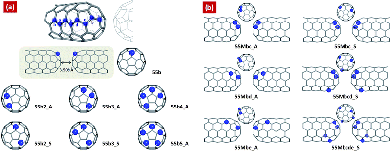 | ||
| Fig. 1 Schematic of the two facing multi-N-doped capped carbon nanotubes according to the number of doped nitrogen atoms and their conformations compared to that of single-N-doped capped CNT(5,5) junction, 55b. Models of (a) have nitrogen atoms at only “b” doping site (b-site_multi-N-doped CNTs), and models of (b) have nitrogen atoms at several doping sites, a,b,c,d and e (multi-site_multi-N-doped CNTs). The models are notified by 55Msn_AS, where “55” means armchair(5,5), “M” means multi-site doping, “s” is nitrogen doping site, “n” mean the number of doped nitrogen atoms, and “AS” indicates aggregated or separated conformation. The distance between two facing multi-N-doped CNTs is fixed to 3.509 Å as described in ref. 63. | ||
In the NEGF approach introduced above, the surface Green's functions describing semi-infinite electrodes attached to the defined device part from the left and right sides are derived using the Hamiltonian and overlap matrices corresponding to each CNT contact. Green's function in this study is given by
| G = (E+S − F − Σ1 − Σ2)−1 | (1) |
 | (2) |
 | (3) |
| T(E) = Tr[Γ1GΓ2G+] | (4) |
3. Results and discussion
A. Geometries of the multi-N-doped capped CNT(5,5)
Fig. 1 shows a schematic of the designed multi-N-doped capped CNT junctions. We consider eight doping sites at each carbon layer from the top layer on the cap, indicated by letters (a–e). The geometry optimization calculations are performed for the designed single-N-doped capped CNT(5,5). Comparison of the evaluated total energies reveals that the nitrogen atom prefers to be located near the cap region (a, b, c and d) rather than the sidewall region (e, f, g and h). (See ESI, Table S1)† Because the hemisphere of fullerene is used as the cap structure, the doped nitrogen atom belongs to one pentagonal ring and two hexagonal rings in the cap region compared to only three hexagonal rings in the side wall region. It means that the nitrogen dopants are more stable if they belong to pentagonal rings, on the other hand the nitrogen atoms stabilize the pentagonal rings. This supports recent results which demonstrate that nitrogen can stabilize neighboring pentagons in fullerene isomers.39 In addition, there is correlation between the structural stability and C–N–C bond angles. If the angle closes to 120°, the structure becomes stable.Albeit the most stable doping site is the fourth carbon layer, d doping site, our investigations of electron transport are mainly focused on the N-doped structures at the cap region, especially (a–e), b doping site, because we found in previous work that 55b junction has good Esaki-like behavior with a very large peak-to-valley ratio, 15.03.63 Therefore, we have increased the number of doped nitrogen atoms at b site in order to investigate how negative differential resistance (NDR) behavior responds to the number of doped nitrogen atoms. Fig. 1(a) show b-site_multi-N-doped CNT junctions according to the number of doped nitrogen atoms and their conformations compared to that of single-N-doped capped CNT(5,5) junction, 55b. The models are notified by 55Msn_AS, where “55” means armchair(5,5), “M” means multi-site doping, “s” is nitrogen doping site, “n” mean the number of doped nitrogen atoms, and “AS” indicates aggregated or separated conformation. The distance between two facing multi-N-doped CNTs is fixed to 3.509 Å. In Fig. 1(b) shows multi-site_multi-N-doped CNT junctions, where we have doped nitrogen atoms at several doping sites, a,b,c,d and e.
B. Electron transport characteristics
Current–voltage (I–V) characteristics of the multi-N-doped capped CNT junctions are compared to that of the single-N-doped CNT(5,5), 55b, and pure CNT(5,5) junctions, as shown in Fig. 2. The remarkable feature emerging from the I–V characteristics is that the tunneling current is dramatically increased by nitrogen doping and a negative differential resistance (NDR) is observed compared to that of pure CNT(5,5) junction. In comparison with the I–V characteristics of the multi-N-doped CNT junctions to that of 55b junction, it is seen that the NDR behavior is conserved or reinforced, and the tunneling current is enhanced by addition of nitrogen atoms. The trend is strong for b-site_multi-N-doped CNT junctions rather than for multi-site_multi-N-doped CNT junctions. However the tendency is not such for all junctions, because the NDR behavior disappears at 55b3_S and 55b5_A junctions. And it is seen in the conformational dependency, in which the junctions having aggregated conformation have enhanced current, while separated conformation gives suppressed current. The difference is clearly seen at 55b2 and 55b3 junctions, where the aggregated conformation (55b2_A and 55b3_A) reinforces the current and NDR behavior, while separated conformation (55b2_S and 55b3_S) suppresses the current and NDR behavior.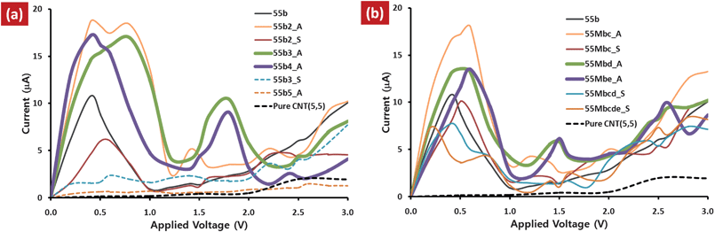 | ||
| Fig. 2 (a) I–V curves of the multi-N-doped capped CNT(5,5) junctions compared to those of the single-N-doped capped CNT(5,5), 55b and pure CNT(5,5) junctions. | ||
The NDR behavior has been known as a typical feature of the Esaki-like diode, i.e. tunneling diode, which provides on (high current) and off (low current) state under gradually increased bias. In the I–V curves, a sharp current peak appears at an applied bias range of 0.0 V < V < 1.0 V, while the current is very low around the 1.0 V < V < 1.5 V applied bias range. The I–V curve shows a relatively large peak-to-valley ratio (PVR), >4, although the height of the sharp current peak and the peak position (Vpeak) depend on designed junctions. The remarkable feature emerging from the results is sequential NDR behavior induced by additional nitrogen atoms and the feature depends on the confromation, aggregated or separated. In b-site_multi-N-doped CNT junctions, 55b2_A, 55b3_A and 55b4_A junctions of aggregated conformation, have another new sharp current peak at 1.5 V < V < 2.0 V applied bias range (Vpeak2) and current valley at 2.0 V < V < 2.5 V applied bias range (Vvalley2). Beside, in the case of multi-site_multi-N-doped CNT junctions, weak new current peak is seen for 55b2_A, 55Mbd_A, and 55Mbe_A. Among the multi-N-doped capped CNT junctions, 55b3_A and 55b4_A junctions provide clear sequential NDR behavior. The observed sequential NDR behavior can be used for successive switching process in which each switching occurs at different times when the bias current is gradually increased as described in Fig. 3.
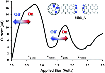 | ||
| Fig. 3 Multi-switching behavior of the multi-N-doped capped CNT(5,5) junction, 55b3_A. | ||
In order to estimate the dependency of the NDR behavior on the distance between two facing CNTs, we have investigated the I–V characteristics at different distances for single-N-doped CNT junction, 55b (see ESI, Fig. S1).† It is seen that the tunneling current is suppressed by increasing the distance and the PVR value depends on the distance. However, the distance of 3.5 Å gives a relatively good performance with regard to peak height and PVR value.
C. The role of the nitrogen dopants for the NDR behavior
Such distinguishable electron transport characteristics usually originate from the intrinsic nature of the molecule, such as the molecular energy level alignment with respect to the Fermi level and their response to the applied bias voltage. Nitrogen is having a profound effect on the structural arrangement and electronic properties of the CNTs, such as a strong donor states near the Fermi level.51–53 with additionally localized nonbonding states of lone pair electrons. It has been reported that a nitrogen atom forms a quasi-tetrahedron with surrounding host atoms through bonding and nonbonding interactions associated with the production of electronic holes and antibonding dipoles.69 These events add features of density of states, such as nonbonding lone pairs, to the valence band of the host material. Therefore, doped nitrogen atoms act as donors with additionally localized nonbonding states of lone pair electrons. Therefore, a small amount of dopants can drastically modify the electronic transport properties of the tube. In this work, our results show the nitrogen dopants correspondingly affect the electron transport characteristics of the multi-N-doped capped CNT junctions through new conducting channels, which is an enhancement of the tunneling current and appearance of NDR behavior. A possible scenario that can lead to NDR behavior at the atomic level was studied theoretically and experimentally. The essential argument is that if there is a weak link between two parts of the conducting system, each of which has relatively narrow features in the density of states in the energy range of interest, the NDR behavior is likely to occur.66 In addition, the NDR behavior can be explained by the filtering effects67,68 of the central device part; the contact of metal electrodes modifies the electronic states of the molecule by filtering the continuous Bloch bands of a contact electrode, accordingly thus only a few filtered energy levels give substantial transmission through a given molecule under the applied biases.In this work, the NDR behavior of the multi-N-doped capped CNT junctions can be explained on the same basis. So, in advance we have investigated the molecular orbitals of one side of the designed junctions. If the molecular orbitals have a contribution to the cap region, they can make available the electron conducting channel between the linked CNTs. In Fig. 4, it is seen that the doped nitrogen atom enhances the contribution of the molecular orbitals at the cap region of HOMOs (HOM-3, -2, -1 and HOMO) and LUMOs (LUMO and LUMO + 1). LUMO + 2 and LUMO + 3 orbitals do not have the contribution of the molecular orbitals at the cap region. Accordingly, two groups of energy levels (HOMOs and LUMOs) generate the HOMO filtered energy levels (HFEL) and the LUMO filtered energy levels (LFEL) through coupling with the semi-infinite CNT electrode. In the case of HFEL, HFEL1 and HFEL2 are possible because of the energy gap between them. Therefore, the NDR behavior in the multi-N-doped capped CNT junctions can be interpreted by a rigid shift model of the LFEL and HFELs in the left and right electrodes under the applied biases. As the applied bias voltage, the alignment between LFEL and HFELs of each electrode gradually increases until the Vpeak due to the fact that the applied bias leads to two different contact chemical potentials, μ1,2 = Ef ∓ eV/2 under the applied biases. When the applied bias reaches the Vpeak1, HFEL1 and LFEL of each electrode are well aligned and a peak appears in the I–V curve. At the Vvalley1, the tunneling current becomes low because of mismatching between HFEL1 and LFEL of each electrode. And then, HFEL2 and LFEL work like HFEL1 and LFEL at Vpeak2 and Vvalley2. However, at higher bias voltage, the alignment between the LFEL (HFEL) and CFEL (VFEL) of each electrode takes place again and the tunneling current increases (Fig. 5).
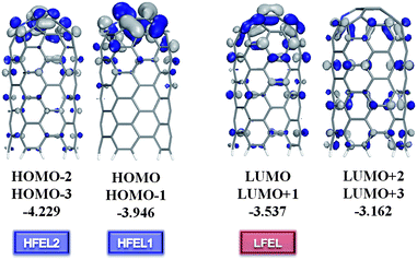 | ||
| Fig. 4 Molecular orbitals of the multi-N-doped capped CNT(5,5), which is one part of 55b3_A junction. Molecular energies (in eV) are calculated at the Perdew–Burke–Ernzerhof/double numerial basis including d-polarization function (PBE/DND) level of theory. “HFEL” and “LFEL” mean HOMO filtered energy level and the LUMO filtered energy level. | ||
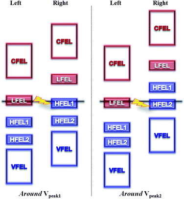 | ||
| Fig. 5 Diagram of the relative shift of the energy levels in the left and right multi-N-doped capped CNTs under applied biases around Vpeak. | ||
The bias dependence of the transmission curve, T(E,V), also gives a clear explanation of the NDR behavior, as seen in Fig. 6. (T(E,V) of 55b3_A is compared to that of pure CNT(5,5) in the ESI. Fig. S2).† The new transmission peaks near the Fermi level induce a sharp current peak in the I–V curve described as white arrows, because the current is the integration of the transmission coefficient within the bias window. However, around the Vvalley, the mismatching between HFELs and LFEL of each electrode causes the generated new transmission peaks to vanish. As seen in 55b3_A and 55b4_A junctions, the sequential NDR behavior can be clearly understood by successive generation of new transmission peaks. Looking at the T(E,V) plots of all designed N-doped capped CNT junctions, it is seen that the generation of new transmission peaks depends on the conformation and the number of doped nitrogen atoms. 55b2_S and 55b3_S junctions have very weak transmission peaks around the Fermi level as compared to 55b2_A and 55b3_S junctions, which is the reason why separated conformation gives a suppressed current. In addition, there is no newly generated transmission peaks around the Fermi level for 55b5_A junction.
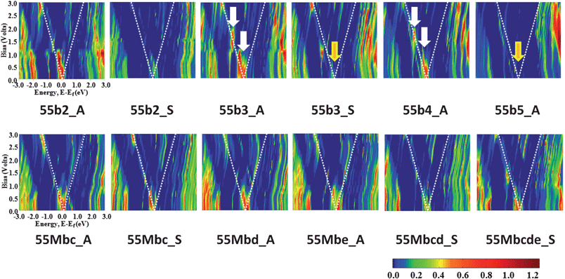 | ||
| Fig. 6 Bias dependence of the transmission curves, T(E,V), calculated at every 0.2 bias voltage: multi-N-doped capped CNT(5,5) junction. Dotted white lines indicate the range of current integration around the Fermi level. White arrows indicate the appearance of new transmission peaks and yellow arrows point to weakened or disappeared transmission peaks. | ||
Therefore, it is worth mentioning that nitrogen dopants modify the molecular orbitals, which generates new conducting channels in the designed multi-N-doped capped CNT junctions by inducing the NDR behavior.
4. Conclusion
We have performed a systematic analysis of electron transport characteristics for the multi-N-doped capped CNT(5,5) junctions at a different number of nitrogen atoms and their doping sites considering conformations, aggregated and separated conformations. The remarkable feature emerging from the I–V characteristics is that the multi-N-doped capped CNT junctions provide multi-switching behavior with sequential negative differential resistance (NDR). Our results show that the conformation and the doping site of nitrogen significantly affect electron transport characteristics; when the multi-N-doped CNT junction has the aggregated conformation and three or four nitrogen atoms are substituted at b doping site, they provide strong NDR and multi-switching behavior. We clearly interpret the NDR behavior using a rigid shift model of the HOMO-filtered energy levels (HFEL) and the LUMO-filtered energy levels (LFEL), where the HOMO-filtered energy levels correspond to the localized nonbonding states of the lone pair electrons induced by nitrogen dopants.It is concluded that the doped nitrogen atom plays an important role in the electron transport characteristics of the designed CNT junctions by modifying their molecular orbitals so as to acieve the NDR behavior. We believe that our results will give an insight into the design and implementation of various electronic logic functions based on carbon nanotubes for applications in the field of nanoelectronics.
Acknowledgements
The authors sincerely thank the crew of the Center for Computational Materials Science of the Institute of Materials Research, Tohoku University, for their continuous support of supercomputing facilities.Notes and references
- T. Pichler, Nat. Mater., 2007, 6, 332 CrossRef CAS.
- Ph. Avouris, Acc. Chem. Res., 2002, 35, 1026 CrossRef CAS.
- O. Zhou, H. Shimoda, B. Gao, S. Oh, L. Fleming and G. Yue, Acc. Chem. Res., 2002, 35, 1045 CrossRef CAS.
- C. Dekker, Phys. Today, 1999, 52, 22 CAS.
- T. Hasobe, S. Fukuzumi and P. V. Kamat, Angew. Chem., Int. Ed., 2006, 45, 755 CrossRef CAS.
- K. S. Novoselov, D. Jiang, F. Schedin, T. J. Booth, V. V. Khotkevich, S. V. Morozov and A. K. Geim, Proc. Natl. Acad. Sci. U. S. A., 2005, 102, 10451 CrossRef CAS.
- G. Y. Zhang, X. Jiang and E. G. Wang, Appl. Phys. Lett., 2004, 84, 2646 CrossRef CAS.
- S. Iijima, M. Yudasaka, R. Yamada, S. Bandow, K. Suenaga, F. Kokai and K. Takahashi, Chem. Phys. Lett., 1999, 309, 165 CrossRef CAS.
- A. Krishman, E. Dujardin, M. M. J. Treacy, J. Hugdahl, S. Lynum and T. W. Ebbesen, Nature, 1997, 388, 451 CrossRef CAS.
- D. Ugarte, Nature, 1992, 359, 707 CrossRef CAS.
- C. N. R. Rao and A. K. Cheetham, J. Mater. Chem., 2001, 11, 2887 RSC.
- A. Bandyopadhyay and S. Acharya, Proc. Natl. Acad. Sci. U. S. A., 2008, 105, 3668 CrossRef CAS.
- P. Liljeroth, J. Repp and G. Meyer, Science, 2007, 317, 1203 CrossRef CAS.
- S. U. Lee, Y.-K. Han, H. Mizuseki and Y. Kawazoe, Chem. Phys. Lett., 2007, 435, 90 CrossRef CAS.
- R. H. M. Smit, Y. Noat, C. Untiedt, N. D. Lang, M. C. van Hemert and J. M. van Ruitenbeek, Nature, 2002, 419, 906 CrossRef CAS.
- J. Reichert, R. Ochs, D. Beckmann, H. B. Weber, M. Mayor and H.v. Löhneysen, Phys. Rev. Lett., 2002, 88, 176804 CrossRef CAS.
- M. A. Reed, C. Zhou, C. J. Muller, T. P. Burgin and J. M. Tour, Science, 1997, 278, 252 CrossRef CAS.
- S. U. Lee, R. V. Belosludov, H. Mizuseki and Y. Kawazoe, Small, 2008, 4, 962 CrossRef CAS.
- S. U. Lee, R. V. Belosludov, H. Mizuseki and Y. Kawazoe, J. Phys. Chem. C, 2007, 111, 15397 CrossRef CAS.
- H. Mizuseki, R. V. Belosludov, T. Uehara, S. U. Lee and Y. Kawazoe, J. Korean Phys. Soc., 2008, 52, 1197 Search PubMed.
- Y. Xue and M. A. Ratner, Phys. Rev. B: Condens. Matter Mater. Phys., 2003, 68, 115406 CrossRef.
- Y. Xue and M. A. Ratner, Phys. Rev. B: Condens. Matter Mater. Phys., 2003, 68, 115407 CrossRef.
- P. S. Damle, A. W. Ghosh and S. Datta, Chem. Phys., 2002, 281, 171 CrossRef CAS.
- M. Brandbyge, J. L. Mozos, P. Ordejón, J. Taylor and K. Stokbro, Phys. Rev. B: Condens. Matter Mater. Phys., 2002, 65, 165401 CrossRef.
- J. L. Mozos, P. Ordejón, M. Brandbyge, J. Taylor and K. Stokbro, Nanotechnology, 2002, 13, 346 CrossRef CAS.
- N. Néel, J. Kröger, L. Limot, T. Frederiksen, M. Brandbyge and R. Berndt, Phys. Rev. Lett., 2007, 98, 065502 CrossRef CAS.
- T. Ono and K. Hirose, Phys. Rev. Lett., 2007, 98, 026804 CrossRef.
- F. OuYang, H. Xu and T. Fan, J. Appl. Phys., 2007, 102, 064501 CrossRef.
- J. J. Palacios, A. J. Pérez-Jiménez and E. Louis, Phys. Rev. B: Condens. Matter Mater. Phys., 2001, 64, 115411 CrossRef.
- J. Taylor, H. Guo and J. Wang, Phys. Rev. B: Condens. Matter Mater. Phys., 2001, 63, 121104 CrossRef.
- A. J. Mieszawska, R. Jalilian, G. U. Sumanasekera and F. P. Zamborini, Small, 2007, 3, 722 CrossRef CAS.
- L. B. Ruppalt and J. W. Lyding, Small, 2007, 3, 280 CrossRef CAS.
- J. A. Misewich, R. Martel, Rh. Avouris, J. C. Tsang, S. Heinze and J. Tersoff, Science, 2003, 300, 783 CrossRef CAS.
- Z. Chen, J. Appenzeller, Y.-M. Lin, J. Sippel-Oakley, A. G. Rinzler, J. Tang, S. Wind, P. Solomon and Rh. Avouris, Science, 2006, 311, 1735 CrossRef CAS.
- W. Zhu and E. Kaxiras, Nano Lett., 2006, 6, 1425 CrossRef.
- V. M. García-Suárez, J. Ferrer and C. J. Lambert, Phys. Rev. Lett., 2006, 96, 106804 CrossRef.
- T. Takenobu, T. Takano, M. Shiraishi, Y. Murakami, M. Ata, H. Kataura, Y. Achiba and Y. Iwasa, Nat. Mater., 2003, 2, 683 CrossRef CAS.
- B. G. Sumpter, V. Meunier, J. M. R. Herrera, E. C. Silva, D. A. Cullen, H. Terrones, D. J. Smith and M. Terrones, ACS Nano, 2007, 1, 369 CrossRef CAS.
- C. P. Ewels, Nano Lett., 2006, 6, 890 CrossRef CAS.
- B. L. Allen, P. D. Kichambare and A. Star, ACS Nano, 2008, 2, 1914 CrossRef CAS.
- F. Villalpando-Paez, A. Zamudio, A. L. Elias, H. Son, E. B. Barros, S. G. Chou, Y. A. Kim, H. Mauramatsu, T. Hayashi, J. Kong, H. Terrones, G. Dresselhaus, M. Endo, M. Terrones and M. S. Dresselhaus, Chem. Phys. Lett., 2006, 424, 345 CrossRef CAS.
- Y. W. Son, J. Ihm, M. L. Cohen, S. G. Louie and H. J. Choi, Phys. Rev. Lett., 2005, 95, 216602 CrossRef.
- C. P. Ewels and M. Glerup, J. Nanosci. Nanotechnol., 2005, 5, 1345 CrossRef CAS.
- X. Blase, J.-C. Charlier, A. D. Vita, R. Car, P. Redlich, M. Terrones, W. K. Hsu, H. Terrones, D. L. Carroll and P. M. Ajayan, Phys. Rev. Lett., 1999, 83, 5078 CrossRef CAS.
- B. G. Sumpter, J. Huang, V. Meunier, J. M. Romo-herrera, E. Cruz-silva, H. Terrones and M. Terrones, Int. J. Quantum Chem., 2009, 109, 97 CrossRef CAS.
- H.-S. Ahn, K.-R. Lee, D.-Y. Kim and S. Han, Appl. Phys. Lett., 2006, 88, 093122 CrossRef.
- M. Doytcheva, M. Kaiser, M. A. Verheijen, M. Reyes-Reyes, M. Terrones and N. Jonge, Chem. Phys. Lett., 2004, 396, 126 CrossRef CAS.
- J.-C. Charlier, M. Terrones, M. Baxendale, V. Meunier, T. Zacharia, N. L. Rupesinghe, W. K. Hsu, N. Grobert, H. Terrones and G. A. J. Amaratunga, Nano Lett., 2002, 2, 1191 CrossRef CAS.
- L. H. Chan, K. H. Hong, D. Q. Xiao, W. J. Hsieh, S. H. Lai, H. C. Shih, T. C. Lin, F. S. Shieu, K. J. Chen and H. C. Cheng, Appl. Phys. Lett., 2003, 82, 4334 CrossRef CAS.
- G. Zhang, W. Duan and B. Gu, Appl. Phys. Lett., 2002, 80, 2589 CrossRef CAS.
- M. Terrones, P. M. Ajayan, F. Banhart, X. Blase, D. L. Carroll, J. C. Charlier, R. Czerw, B. Foley, N. Grobert, R. Kamalakaran, P. Kohler-Redlich, M. Rühle, T. Seeger and H. Terrones, Appl. Phys. A: Mater. Sci. Process., 2002, 74, 355 CAS.
- R. Czerw, M. Terrones, J.-C. Charlier, X. Blase, B. Foley, R. Kamalakaran, N. Grobert, H. Terrones, D. Tekleab, P. M. Ajayan, W. Blau, M. Rühle and D. L. Carroll, Nano Lett., 2001, 1, 457 CrossRef CAS.
- D. L. Carroll, Ph. Redlich, X. Blase, J.-C. Charlier, S. Curran, P. M. Ajayan, S. Roth and M. Rühle, Phys. Rev. Lett., 1998, 81, 2332 CrossRef CAS.
- Y. Liu and H. Guo, Phys. Rev. B: Condens. Matter Mater. Phys., 2004, 69, 115401 CrossRef.
- S. Latil, S. Roche, D. Mayou and J.-C. Charlier, Phys. Rev. Lett., 2004, 92, 256805 CrossRef.
- H. J. Choi, J. Ihm, S. G. Louie and M. L. Cohen, Phys. Rev. Lett., 2000, 84, 2917 CrossRef CAS.
- V. Krstić, S. Blumentritt, J. Muster, S. Roth and A. Rubio, Phys. Rev. B: Condens. Matter Mater. Phys., 2003, 67, 041401 CrossRef.
- C.-C. Kaun, B. Larade, H. Mehrez, J. Taylor and H. Guo, Phys. Rev. B: Condens. Matter Mater. Phys., 2002, 65, 205416 CrossRef.
- K. Liu, Ph. Avouris, R. Martel and W. K. Hsu, Phys. Rev. B: Condens. Matter Mater. Phys., 2001, 63, 161404 CrossRef.
- S. U. Lee, M. Khazaei, F. Pichierri and Y. Kawazoe, Phys. Chem. Chem. Phys., 2008, 10, 5225 RSC.
- M. Khazaei, S. U. Lee, F. Pichierri and Y. Kawazoe, ACS Nano, 2008, 2, 939 CrossRef CAS.
- M. Khazaei, S. U. Lee, F. Pichierri and Y. Kawazoe, J. Phys. Chem. C, 2007, 111, 12175 CrossRef CAS.
- S. U. Lee, R. V. Belosludov, H. Mizuseki and Y. Kawazoe, Small, 2009, 5, 1769 CrossRef CAS.
- J. P. Perdew, K. Burke and M. Ernzerhof, Phys. Rev. Lett., 1996, 77, 3865 CrossRef CAS.
- N. Troullier and J. L. Martins, Phys. Rev. B: Condens. Matter, 1991, 43, 8861 CrossRef.
- Y. Xue, S. Datta, S. Hong, R. Reifenberger, J. I. Henderson and C. P. Kubiak, Phys. Rev. B: Condens. Matter Mater. Phys., 1999, 59, R7852 CrossRef CAS.
- X. Zheng, X. Shi, Z. Dai and Z. Zeng, Phys. Rev. B: Condens. Matter Mater. Phys., 2006, 74, 085418 CrossRef.
- C.-C. Kaun, H. Guo, P. Grütter and R. B. Lennox, Phys. Rev. B: Condens. Matter Mater. Phys., 2004, 70, 195309 CrossRef.
- W. T. Zheng and C. Q. Sun, Prog. Solid State Chem., 2006, 34, 1 CrossRef CAS.
Footnote |
| † Electronic supplementary information (ESI) available: Relative energies and average C–N–C bond angles of the single-N-doped capped CNT(5,5) at the PBE/DND level of theory (Table S1); I–V curves of 55b junction at the different distances of the two facing N-doped capped CNTs (Fig. S1);Bias dependence of the transmission curves, T(E,V), calculated at every 0.5 bias voltage: pure and multi-N-doped capped CNT(5,5) junction, 55b3_A (Fig. S2). See DOI: 10.1039/c0nr00411a |
| This journal is © The Royal Society of Chemistry 2010 |