Slope-tunable Si nanorod arrays with enhanced antireflection and self-cleaning properties
Yi-Ruei
Lin
a,
K. Y.
Lai
a,
Hsin-Ping
Wang
a and
Jr-Hau
He
*ab
aInstitute of Photonics and Optoelectronics, National Taiwan University, Taipei, 10617, Taiwan, ROC. E-mail: jhhe@cc.ee.ntu.edu.tw
bDepartment of Electrical Engineering, National Taiwan University, Taipei, 10617, Taiwan, ROC
First published on 8th October 2010
Abstract
Slope-tunable Si nanorod arrays (NRAs) were fabricated with colloidal lithography and reactive ion etching (RIE). Sharpened NRAs fabricated by increasing the SF6/O2 flow ratio during RIE exhibit enhanced antireflection (AR) and hydrophobic properties, which are attributed to the smooth gradient in the effective refractive index of NRAs, and the enlarged water/air interface of the water drops in the NRA layers, respectively. Enhanced AR characteristics via modifying the slope of NRAs are accompanied by broad-band working ranges, omnidirectionality, and polarization insensitivity. Detailed experimental and theoretical analysis of slope-tunable NRAs should benefit the development of various self-cleaning optoelectronic devices with efficient light management.
Introduction
Among the numerous materials eligible for photovoltaic applications, Si is the most popular candidate due to its abundance on earth and the well-established processes. However, the very different refractive indices between air and Si cause more than 30% of the incident light to be reflected back from the surface of a Si-based solar cell.1 In order to suppress the undesired reflections, an additional layer with a thickness of quarter-wavelength is usually employed as the antireflection coating (ARC). However, the ARC obtained in this way encounters two major problems: (i) the reflectance only reaches the minimum at a single wavelength (λmin), and gradually increases as the wavelength deviates from λmin,2 and (ii) the adhesion and the thermal stability of the ARC are generally unsatisfactory due to the mismatch of material properties between the ARC and Si.3 Antireflective nanorod arrays (NRAs), inspired by moth-eye corneas which comprise of periodic arrays of protuberance,4 have been demonstrated as an alternative to attain superior antireflection (AR) performances, including broad-band working ranges,5 omnidirectionality,6 and polarization insensitivity.6 The advantages of these biomimetic structures are mainly attributed to the subwavelength dimensions of the NRAs, which make the nanostructures behave like a homogeneous medium with an intermediate refractive index (neff), effectively decreasing the discontinuity of the air/Si interface and thereby eliminating the reflection.4–6Thanks to the advance in nanofabrication techniques, various Si-based nanostructures with excellent AR performances have been successfully demonstrated.5–13 Among the published results, it is found that the NRAs exhibiting significantly reduced reflectance usually contain the lengths on the order of l μm or longer.6,8 As long NRAs generally require additional material cost or process times, reducing the length of NRAs yet preserving quality AR performance is desirable for practical applications. Recently, it has been reported that smoothening the gradient of NRAs' neff, namely replacing nanorods with nanocones, would result in further reduced reflectance.14,15 However, the study regarding the link between the extent of slope change of NRAs and the corresponding AR properties remains limited. In addition, the responses of nanocones to different light polarizations, which are of great importance to ARC, are also rarely reported.
Another example of biomimetic engineering is the self-cleaning effect by the formation of the hydrophobic surface, originally observed on water-repellent lotus leaves and butterfly wings. The hydrophobicity of the surface can be conveniently enhanced by the nanostructured surfaces and strongly depends on the geometry of nanostructures.16 The surface features combining AR and super-hydrophobic effects allow the optoelectronic devices to stay away from contamination so that the efficiency is maintained. Although the hydrophobic properties of nanostructured surfaces were studied by several groups,16–18 there have been limited reports on the dependence of surface hydrophobicity on the NRAs' slopes.
In this study, slope-tunable NRAs with 360 nm in height are successfully fabricated with colloidal lithography and reactive ion etching (RIE). The fabrication techniques presented here are IC-compatible and avoid the use of expensive and complex equipment. The fabricated NRAs exhibit superior AR properties with broad-band, omnidirectional, and polarization-insensitive characteristics. The enhancement of the hydrophobic effect via modifying the slope of NRAs is also demonstrated. This study will be beneficial for the design of a wide variety of self-cleaning optoelectronic devices with efficient light management by controlling the structure profile of the nanostructures.
Experiments
Self-assembly colloidal lithography and RIE were used to fabricate the NRAs. In the process, Si substrates were drop-coated with close-packed polystyrene (PS) nanospheres with a diameter of 500 nm. The drop coating process was carried out with the following procedures. To produce a monolayer of PS nanospheres, the Si substrate surface was made hydrophilic by the immersion in a solution of H2SO4/H2O2 at 80 °C for 10 min. The PS-nanosphere solution diluted in deionized (DI) water was then coated on the substrate surface with a volume-controlled pipette. Finally the substrate was held at 50 °C and 87.5% relative humidity for 2 h, and a close-packed hexagonal PS monolayer was formed upon drying the solution. The PS monolayer was uniformly distributed within the area of ∼1.5 mm2, and the period (center-to-center distance) of the close-packed nanospheres is 500 nm. The slope-tunable nanorod structures were achieved by a one-step RIE process employing the mixture of SF6 and O2 with the PS nanospheres acting as the etching masks. The slopes of NRAs were controlled by varying the SF6/O2 flow ratio. With the O2 flow fixed at 5 sccm, three SF6/O2 flow ratios were adopted: 1.5, 2.0, and 4.0. The etching time of the RIE process was 90 s for the three samples.In order to further tilt the edges of nanorods, another sample was prepared by a two-step RIE process, in which 50 sccm O2 plasma was firstly used to shrink the diameter of PS nanospheres, followed by etching with a mixture of SF6/O2 (12.5/5 sccm) plasma for 45 s. The produced NRAs were to be used to compare with the three samples fabricated by the one-step RIE process.
Morphologies of the NRAs were observed using scanning electron microscopy (SEM, field emission JEOL JSM-6500) with an acceleration voltage of 10 kV. Reflection measurements were performed with a JASCO V-670 UV-vis spectrometer equipped with an integral sphere.
Results and discussion
Fig. 1(a) shows a typical SEM image of a monolayer of the hexagonally close-packed PS nanospheres on the Si substrates. The Si NRAs fabricated with the SF6/O2 flow ratio of 1.5, 2.0, and 4.0 are shown in Fig. 1(b)–(d), and the NRAs made by the two-step RIE process are shown in Fig. 1(e). The geometric profiles of NRAs depend strongly on the ratio of the gas mixtures, the coil power, and the working pressure of RIE. In this work, the coil power and the working pressure for all the samples were fixed at 50 W and 1.33 mTorr, respectively. Since the vertical etching rate is insensitive to the ratio of gas mixtures when the coil power is as low as 50 W,19 the heights of the NRAs shown in Fig. 1(b)–(d) are all around 360 nm under the same etching duration (90 s). On the other hand, the height of the NRAs in Fig. 1(e) is only 200 nm, mimicking the moth eye structure by exhibiting the most tilted edge as compared with the three other samples. During the etching process in the SF6/O2 plasma, the active fluorine ions provide the etching effect of Si by forming the volatile SiF4, while the oxygen ions passivate the Si surface with SiOxFy.20 This suggests that the shape of the nanostructures can be tailored by adjusting the SF6/O2 flow ratio to reach a certain balance between the etching and the passivation. For example, the sharp NRAs (or nanocones), shown in Fig. 1(c) and 1(d), can be obtained by increasing the SF6 flow to introduce a moderate undercut below the etching mask.21 On the other hand, the structures with nearly vertical walls, shown in Fig. 1(a), can be obtained by decreasing the SF6/O2 flow ratio to avoid the undercut effect. The effective refractive index (neff) gradient of the NRAs can be estimated by the equation proposed by Stavenga et al.:22| neff(h) = {f(h)nqSi + [1 − f(h)]nqair}1/q | (1) |
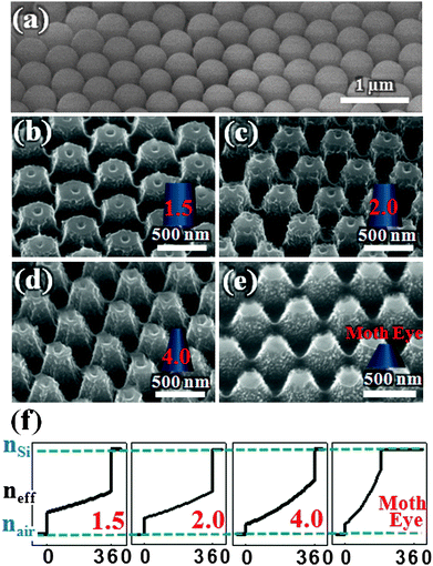 | ||
| Fig. 1 SEM images of (a) 500 nm PS nanosphere monolayer, Si NRAs fabricated with the SF6/O2 flow ratio of (b) 1.5, (c) 2, (d) 4, and (e) the moth eye structure. (f) Calculated effective refractive index (neff) profiles of Si NRAs fabricated with different SF6/O2 flow ratios and the moth eye structure. | ||
Fig. 2 presents the total reflectance of polished Si surfaces and the four types of NRAs in the wavelengths ranging from 350 to 850 nm. The incident angle was fixed at 8° during the measurements. For the polished Si, most of the reflectance is greater than 35% over the studied wavelengths due to the large refractive index discontinuity at the air–Si interface. In contrast, the NRAs exhibit broad-band reflectance as low as 6%. Conventionally, a single-layer ARC with one-quarter wavelength of interest achieves very low narrowband reflectance by exploiting the interference of light reflected from the two interfaces. In our NRAs, the continuous change in neff causes the incident light to be reflected at different depths from the interface of air and ARCs, the significant suppression of broad-band reflectance can occur through destructive interferences, where the waves with different phases partially or wholly cancel one another. Therefore, the gradient of refractive index of the ARCs, an index transition from air to Si (i.e., from a low to a high index material), is effective in the reflection elimination. Furthermore, the NRAs combining a refractive index gradient with the smallest discontinuities at both interfaces are expected to exhibit the most effective reflection elimination, which explains the low reflectance of the NRAs obtained by the SF6/O2 ratio of 4.0, as compared with the NRAs with the SF6/O2 ratio of 1.5 and 2.0. The significant decrease in the reflectance of Si NRAs can also be related to the periodic subwavelength structures, eliminating the diffraction-order light, and thus reducing the reflectance.23 It is noticed that the moth eye-like structure, even with less height, produces reflectance lower than that on the NRAs by SF6/O2 = 4.0 for most of the wavelength ranges. The stronger peak at 370 nm of the moth eye-like structure is presumably due to the relatively efficient interband transitions in Si.24 The result indicates that increasing the extent of nanorod-edge tilting, and therefore the grading in NRAs' neff, are beneficial for the suppression of reflectance.
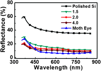 | ||
| Fig. 2 Total reflectance measured over the wavelengths ranging from 350 to 850 nm with polished Si substrates, the NRAs fabricated with different SF6/O2 flow ratios, and the moth eye structure. | ||
To investigate the omnidirectional characteristics of the Si NRAs, the specular reflectance with the angles of incidence (AOI's) from 10 to 80° was measured with polished Si and slope-controlled Si NRAs for unpolarized, s-, and p-polarized light shown in Fig. 3. The wavelength was fixed at 650 nm during the measurements. Generally, the reflectance is reduced by increasing the ratio of SF6/O2, and the moth eye structure reaches the lowest reflectance for most of the AOI's. The reflectance of the moth eye structure remains below 3.5% (unpolarized), 8.0% (s-polarized), and 0.8% (p-polarized) for the AOI's up to 50°. These values are lower than those of polished Si surface by more than 5 times, indicating that sharpening the NRAs can effectively improve the omnidirectionality of the nanostructured surface. It is noticed that the reflectance of all the Si NRAs is increased significantly after AOI reaches 60°. Similar results were also observed elsewhere.25 Intuitively, when the light reaches the NRA layer's surface at a large AOI, the portion of the light entering the NRA layers is decreased, and thus the light trapped within the NRA layers is reduced, leading to an increase of the reflectance. The polarization-dependent omnidirectionality can be characterized by the ratio of the reflectance of the s-polarization to that of the p-polarization (Is/Ip), as shown in Fig. 3(d). The polished Si exhibits a maximum of Is/Ip over 130 at 76° while Is/Ip is decreased significantly to <16 for all NRAs, suggesting the reflection becomes polarization-insensitive in nanorod structures. The AOI- and polarization-insensitive AR characteristics can be attributed to the interference effects which result from the gradient of refractive index.26 In Fig. 3(d), it is also noticed that Brewster's angle shifts from 76° on the polished surface to 52°∼60° at the nanostructured surfaces. The shift is likely to be caused by the incoherent multiple scattering on a rough surface.27
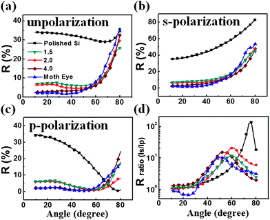 | ||
| Fig. 3 Specular reflectance as a function of AOI measured with the NRAs fabricated with different SF6/O2 flow ratios and the moth eye structure using (a) unpolarized, (b) s-polarized, and (c) p-polarized light of 650 nm wavelength. (d) The reflectance ratio of s polarization to p polarization (Is/Ip) as a function of AOI. | ||
The hydrophobicity of the slope-controlled Si NRAs was characterized by the contact angles (CAs) of water drops on the NRA surfaces. In order to evaluate exclusively the effect of edge slope on the surface hydrophobicity, we only compared the CAs on the NRAs with similar height, i.e. 360 nm. The CA on the polished surfaces of Si substrates is 95°, and those measured on the NRAs fabricated with different SF6/O2 ratios are shown in Fig. 4. The corresponding photographs of water droplets on different NRA surfaces are shown in the insets of Fig. 4. It is evident that the CA is increased continuously with SF6/O2 ratio. With SF6/O2 = 4, CA can be as large as 122°. The results indicate that surface hydrophobicity of the NRAs is enhanced when the nanorods become sharp. The slope-dependent hydrophobic behavior of the NRA surfaces can be explained by Cassie's equation:28
| cosθw = fcosθy − (1 − f) | (2) |
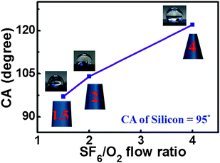 | ||
| Fig. 4 The magnitude of CA for the slope-controlled NRAs as a function of SF6/O2 flow ratio. The insets are corresponding photographs of water droplets on the surface of NRAs. | ||
Conclusion
Without depositing any additional ARCs, Si NRAs fabricated by colloidal lithography and RIE provide impedance matching between Si and air through a gradient of the neff. The index discontinuity between air to Si substrates can be decreased with the SF6/O2 flow ratio during the one-step RIE process, and the NRAs with further tilted edges can be obtained with the two-step RIE process. The reflection is greatly eliminated over a wide range of wavelengths and AOI's; for example, the NRAs with the most tilted edges (the moth eye structure) produce total reflectance as low as 6% in the wavelengths of 350–850 nm, and keep the specular reflectance below 3.5% for AOI's up to 50° with unpolarized 650 nm light. Is/Ip is decreased to less than 16 for all NRA layers, demonstrating polarization-insensitive AR characteristics. In addition, hydrophobic properties were also enhanced by modifying the slope of the NRAs. The understanding of AR and self-cleaning effects on the geometrical configurations of Si NRAs provides an insight into the performance enhancement of Si-based nanostructured optoelectronic devices.Acknowledgements
The research was supported by the National Science Council Grant No. NSC 99-2112-M-002-024-MY3, NSC 99-2622-E-002-019-CC3, and Aim for Top University Project from the Ministry of Education.References
- P. Doshi, G. E. Jellison and A. Rohatgi, Appl. Opt., 1997, 36, 7826 CrossRef CAS.
- C. G. Someda, Electromagnetic Waves, Chapman & Hall: London, 1998 Search PubMed.
- K. Rahmoun, A. Lost, V. Keryvin, G. Guillemot and N. E. Chabane Sari, Thin Solid Films, 2009, 518, 213 CrossRef CAS.
- P. B. Clapham and M. C. Hutley, Nature, 1973, 244, 281–282.
- C. H. Sun, P. Jiang and B. Jiang, Appl. Phys. Lett., 2008, 92, 061112 CrossRef.
- Y. F. Huang, S. Chattopadhyay, Y. J. Jen, C. Y. Peng, T. A. Liu, Y. K. Hsu, C. L. Pan, H. C. Lo, C. H. Hsu, Y. H. Chang, C. S. Lee, K. H. Chen and L. C. Chen, Nat. Nanotechnol., 2007, 2, 770 CrossRef CAS.
- J. Y. Huang, X. D. Wang and Z. L. Wang, Nano Lett., 2006, 6, 2325 CrossRef CAS.
- Y. Li, J. Zhang, S. Zhu, H. Dong, Z. Wang, Z. Sun, J. Guo and B. J. Yang, J. Mater. Chem., 2009, 19, 1806 RSC.
- X. Fang, Y. Bando, C. Ye, G. Shen, U. K. Gautam, C. Tang and D. Golberg, Chem. Commun., 2007, 4093 RSC.
- X. Fang, Y. Bando, U. K. Gautam, C. Ye and D. Golberg, J. Mater. Chem., 2008, 18, 509 RSC.
- X. Fang, Y. Bando, U. K. Gautam, T. Zhai, H. Zeng, X. Xu, M. Liao and D. Golberg, Crit. Rev. Solid State Mat. Sci., 2009, 34, 190 Search PubMed.
- J. Wang, X.-J. Wang, Y. Jiao, M.-W. Chu, M. Malac and Q. Li, Nanoscale, 2010, 2, 681 RSC.
- Q. Cheng, E. Tam, S. Xu and K. (Ken) Ostrikov, Nanoscale, 2010, 2, 594 RSC.
- J. Zhu, Z. Yu, G. F. Burkhard, C.-M. Hsu, S. T. Connor, Y. Xu, Q. Wang, M. McGehee, S. Fan and Y. Cui, Nano Lett., 2009, 9, 279 CrossRef CAS.
- Y.-L. Chueh, Z. Fan, K. Takei, H. Ko, R. Kapadia, A. A. Rathore, N. Miller, K. Yu, M. Wu, E. E. Haller and A. Javey, Nano Lett., 2010, 10, 520 CrossRef CAS.
- W.-L. Min, B. Jiang and P. Jiang, Adv. Mater., 2008, 20, 3914 CrossRef CAS.
- L. F. Sun, X. Gao and L. Jiang, Acc. Chem. Res., 2005, 38, 644 CrossRef CAS.
- Y. Ding, S. Xu, Y. Zhang, A. C. Wang, M. H. Wang, Y. Xiu, C. P. Wong and Z. L. Wang, Nanotechnology, 2008, 19, 355708 CrossRef.
- E.-Z. Liang, C. J. Huang and C. F. Lin, 4th IEEE Conference on Nanotechnology, 2004 Search PubMed TU-P42.
- H. Janse, M. de Boer, J. Burger, R. Legtenberg and M. Elwenspoek, Microelectron. Eng., 1995, 27, 475 CrossRef.
- X. Wang, W. Zeng, G. Lu, O. L. Russo and E. Eisenbraun, J. Vac. Sci. Technol., B, 2007, 25, 1376 CrossRef CAS.
- D. G. Stavenga, S. Foletti, G. Palasantzas and Arikawa, Proc. R. Soc. London, Ser. B, 2006, 273, 661 CrossRef CAS.
- J. Jahns, Laser Part. Beams, 1999, 17 Search PubMed.
- S. Adachi, J. Appl. Phys., 1989, 66, 3224 CrossRef CAS.
- Y. Kanamori, M. Sasaki and K. Hane, Opt. Lett., 1999, 24, 1422 Search PubMed.
- D. Poitras and J. A. Dobrowolski, Appl. Opt., 2004, 43, 1286 CrossRef.
- J.-J. Greffet, Opt. Lett., 1992, 17, 238 Search PubMed.
- A. B. D. Cassie and S. Baxter, Trans. Faraday Soc., 1944, 40, 546 RSC.
| This journal is © The Royal Society of Chemistry 2010 |