From nucleation to nanowires: a single-step process in reactive plasmas
Kostya (Ken)
Ostrikov
*ab,
Igor
Levchenko
ab,
Uros
Cvelbar
c,
Mahendra
Sunkara
d and
Miran
Mozetic
c
aPlasma Nanoscience Centre Australia (PNCA), CSIRO Materials Science and Engineering, P.O. Box 218, Lindfield, NSW 2070, Australia. E-mail: Kostya.Ostrikov@csiro.au.; Fax: +61-2-94137200; Tel: +61-2-94137634
bPlasma Nanoscience, School of Physics, The University of Sydney, Sydney, NSW 2006, Australia
cJozef Stefan Institute, 39 Jamova cesta, Ljubljana, SI-1000, Slovenia
dChemical Engineering and Conn Center for Renewable Energy Research, University of Louisville, Louisville, Kentucky 40292, USA
First published on 18th August 2010
Abstract
This feature article introduces a deterministic approach for the rapid, single-step, direct synthesis of metal oxide nanowires. This approach is based on the exposure of thin metal samples to reactive oxygen plasmas and does not require any intervening processing or external substrate heating. The critical roles of the reactive oxygen plasmas, surface processes, and plasma-surface interactions that enable this growth are critically examined by using a deterministic viewpoint. The essentials of the experimental procedures and reactor design are presented and related to the key process requirements. The nucleation and growth kinetics is discussed for typical solid–liquid–solid and vapor–solid–solid mechanisms related to the synthesis of the oxide nanowires of metals with low (Ga, Cd) and high (Fe) melting points, respectively. Numerical simulations are focused on the possibility to predict the nanowire nucleation points through the interaction of the plasma radicals and ions with the nanoscale morphological features on the surface, as well as to control the localized ‘hot spots’ that in turn determine the nanowire size and shape. This generic approach can be applied to virtually any oxide nanoscale system and further confirms the applicability of the plasma nanoscience approaches for deterministic nanoscale synthesis and processing.
 Kostya (Ken) Ostrikov | Kostya (Ken) Ostrikov is CEO Science Leader and a founding leader of the Plasma Nanoscience Center Australia at CSIRO Materials Science and Engineering. His achievements include 270 refereed journal papers, more than 80 plenary, keynote, and invited talks at international conferences. His main research program on nanoscale control of energy and matter in plasma–surface interactions contributes to the solution of the grand and as-yet-unresolved challenge of directing energy and matter at the nanoscale, a challenge that is critical for the development of renewable energy and energy-efficient technologies for a sustainable future. |
 Igor Levchenko | Igor Levchenko is a CSIRO CEO Science Leader Senior Research Scientist and Team Leader of the Plasma Nanoscience group. He received his MSc and PhD degrees from the National Airspace University, Ukraine, in 1989 and 1996, respectively. Over the past ten years, he has published over 60 papers in refereed international journals. His research interests include experimental and theoretical nanoscience, nanofabrication (carbon nanotubes, graphene, nanowires, nanodot arrays, semiconductor solar cells), surface science, materials science, and plasma physics. |
 Uros Cvelbar | Uros Cvelbar received his BSc degree in Physics (in 2000) and his PhD degree in Material Science and Plasma Technologies (in 2005) from the University of Ljubljana. He teaches in several European Universities and is Senior Research Scientist at the Jozef Stefan Institute in Ljubljana, Slovenia. His bibliography includes 12 patents, and more than 70 scientific papers published in international journals. His scientific research interests cover areas from material science to plasma technologies including nanotechnology, nanofabrication, nanostructures and their applications. |
 Mahendra Sunkara | Mahendra Sunkara, is a professor in the Chemical Engineering Department and Interim Director of Conn Center for Renewable Energy. He received his BTech, MSc and PhD degrees from Andhra University (India) in 1986, Clarkson University in 1988 and Case Western Reserve University in 1993, respectively. He has published over 100 articles in refereed journals and holds five US patents. He received the NSF CAREER Award in 1999 and the distinction of top 25 young guns in Louisville by Louisville Magazine. His main interests involve diamond, gallium nitride, nanowires and other nanoscale materials as well as their applications. |
 Miran Mozetic | Miran Mozetic received his BSc in physics from the University of Ljubljana, Slovenia, in 1988, and his PhD degree from the University of Maribor, Slovenia, in 1997. Since 2009 he has been the Head of Department of Surface Engineering and Optoelectronics at the Jozef Stefan Institute, Ljubljana and Professor of plasma technology at the JS International Postgraduate School. He is the author of more than 130 scientific papers, and over 10 patents. His main research interests concern the study and development of plasma sources as well as interaction of non-equilibrium plasma with solid materials. |
1. Introduction – setting the scope
This article uses a deterministic viewpoint to approach the problem of rapid and catalyst-free synthesis of one-dimensional metal oxide nanostructures. Metal oxides are among the most ubiquitous materials in natural and industrial environments. This abundance is dictated by the fact that many such materials can be formed by a very simple oxidation in open air. However, some amount of energy, such as heating or flame is usually required to make this process fast and effective. Examples of the nanostructures of our interest include but are not limited to nanotubes, nanowires, nano-pipettes, tip- and needle-like structures and several others. These inorganic one-dimensional nanostructures find numerous applications in fields as diverse as catalysis, energy conversion and storage, environmental sensors, and cancer therapies. The diversity of these applications is determined by the uniqueness and the variety of their chemical, electronic, optical, and other properties. This is why these nanomaterials have recently been of a very significant interest from both the fundamental and applied aspects, which in turn led to the very strong representation of this topic in multidisciplinary literature (see, e.g.1–63 and references therein). Representative scanning electron micrographs of nanowires made of various inorganic materials are shown in Fig. 1.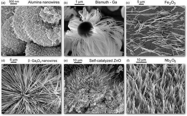 | ||
| Fig. 1 Representative inorganic nanowires synthesized in laboratories of the authors of this article using reactive plasmas. Nanowires (a), (b), (d), and (e) are synthesized through the SLS mechanism using molten microparticles whereas nanowires (c) and (f) are synthesized by direct exposure of iron (c) and niobium (f) foils to reactive oxygen plasmas, through the VSS mechanism. All images except (b) represent metal oxide nanowires. | ||
Compared to common bulk metal oxide materials, reduction of material sizes to nanometre dimensions brings about many new exciting opportunities such as tunable electronic structure, highly-unusual chemical reactivity, substantially improved or even dramatically changed electron/exciton and heat transport properties, as well as the ability to host foreign molecules (e.g., hydrogen). Another exciting opportunity emerges because of the availability of two atomic species, M (metal) and O (oxygen), which can be mixed in virtually any proportions as well as arranged in a variety of atomic stacks with multiple unique options for mutual positioning, coordination, and bonding of the constituent atoms.64,65 These virtually unlimited possibilities in turn depend on the specific material, size, and dimensionality of the nanoscale system considered. As a result, many new and highly-unusual properties can be created by design. For instance, by tuning relative concentrations of metal and oxygen atoms, one can switch between the electronic (n-type) and hole (p-type) conductivity; these relative concentrations strongly depend on the surface-to-volume-ratios and other characteristics of the nano-oxide materials.
These factors underpinned numerous applications of nano-oxide materials in nanoelectronics (oxide barrier layers), optoelectronics (lasing, light emitting diodes, (LEDs)), photovoltaics (transparent conducting oxides (TCOs), functional layers in dye-sensitized solar cells, etc.), biomedicine (nanostructured coatings of biocompatible surgical implant materials, micro-arrays for intracellular drug and gene delivery), electrochemical energy generation and storage (fuel cells, Li-ion batteries, supercapacitors, etc.), self-cleaning nanostructured coatings, environmental sensors (e.g., highly-sensitive low-dose oxygen detection), as well as several other areas.1,2,4,8,10,15,18,27,38,40,53 Most recent examples also include in vivo antioxidants, viral detection and inactivation, spintronics, as well as targeted cancer therapy in nanomedicine.66–68 It is very interesting that the natural abundance of oxide materials makes their nanoscale phases among the most reliable and safest nanomaterials from the nano-toxicity and nano-safety points of view.69
The focus of this article is on the effective plasma-based, single-step approach for the synthesis of one-dimensional metal oxide nanomaterials directly on the surface of a thin metal sample. This approach has recently been applied to a large number of metal oxide systems (see, e.g.2,9,12,16,18,20,22,24,26 and references therein). However, the understanding of the basic mechanisms leading to the nanowire nucleation and growth still remains essentially incomplete. Not surprisingly, the most recent review on plasma-based synthesis of inorganic nanomaterials stated that “there is some unresolved magic in this mechanism”.3 To reveal this “magic”, we will consider this issue by using a deterministic viewpoint6 and follow the main stages and elementary processes involved, starting from the nucleation to the developed arrays of one-dimensional nanostructures. This step-by-step approach relies on the basic understanding of the elementary physical and chemical processes that take place at the most fundamental, atomic, level, followed by the elaboration of specifications of macroscopic synthesis processes.
In the following sections, we will present the rationale of the plasma-based metal oxide nanowire synthesis approach in the same way, step-by-step, by unveiling its essentials through the deterministic consideration of the materials science (Sec. 2) and plasma physics/chemistry (Sec. 3) perspectives. In Sec. 4, we will describe typical experimental procedures involved in the direct plasma synthesis of metal oxide nanowires. In Sec. 5 and 6, we will discuss two examples of the SLS growth of GaO and CdO nanostructures of easy-to-melt metals and one example of the VSS growth of Fe2O3 nanowires. In Sec. 7, we will also present the results of numerical simulations to determine the probable nucleation sites of the nanowires as well as to map the distributions of microscopic ion fluxes over the surfaces of the substrate and the nanowires. This article concludes with the summary of the most important points and the outlook for the future research in Sec. 8.
2. Deterministic approach – materials science perspective
Starting from the atomic level, one should aim at combining two atomic (metal and oxygen) species in the desired proportion, which, depending on the intended application, does not necessarily need to be stoichiometric. Deficiency of either atomic species may lead to new and highly-unusual properties, such as the reversal of electric current conductivity mechanisms, relative importance of dielectric, semiconducting and magnetic properties.More specifically aiming at the growth of metal oxide nanowires, one should specify where exactly do the M and O atoms need to combine. In other words, the nanostructures should nucleate in small localized areas and then emerge as one-dimensional structures, keeping the desired chemical structure and the relative presence of constituent atomic species. For example, ordered two-dimensional arrays of single-crystalline nanotube/nanowire structures are often required to produce and amplify regular responses in electronic, optoelectronic, and sensor devices.
The most common approach to synthesize inorganic nanotubes and nanowires is based on using metal catalyst nanoparticles.1,2,4,25 These particles play two main functions.25 First, they reduce the energy barrier for the incorporation of the growth species into the one-dimensional nanostructure. Second, the nanoparticles localize the nanowires in the lateral direction; in most cases the sizes of the catalyst particles and the nanowires in the substrate plane are very close. The catalyst is usually chosen from those elements that do not easily bond with the constituent atoms of the nanostructure; a reasonable solubility of the latter atoms in the catalyst is also desirable. In many cases the nanowires grow in the tip growth mode, with the catalyst on top. During the growth process, the atoms of the building material(s) (which will also be referred below as the building units, BUs) penetrate into the one-dimensional structure through the above catalyst particle and then stack in one of the nanocrystal growth planes. If a crystalline nanowire predominantly grows in the [100] direction, the BUs preferentially stack into the corresponding {100} crystal planes. The surface energy (per unit area) of the preferential growth plane is then much higher compared to other nanowire surfaces (facets), e.g., {110} and {111}. This is why according to the Wulff's principle the area of the lateral surfaces can increase much faster than the area of the top (growth) surface.51
However, these catalysts are very undesirable, and for several reasons. The main reason is the necessity of at least two additional process stages, namely, initial deposition of metal catalyst nanoparticles and then their removal. Moreover, one has to take constant care about conditioning of this catalyst nanoparticle. Indeed, catalyst “poisoning” (which happens when the ability of the catalyst nanoparticle to support surface/bulk diffusion of BUs is substantially compromised, e.g., by full coverage of its surface with a continuous amorphous layer of the nanowire building material) can easily terminate the growth. There are many other catalyst-related issues such as nanowire nucleation at the nanoparticle edges, which leads to the growth sideways,70 highly-unpredictable supersaturation which then results in non-simultaneous nucleation of the nanowires on different catalyst nanoparticles71 and some others. Moreover, catalyst nanoparticle size, composition, morphology and structure needs to be precisely engineered to achieve certain nanowire properties.
For example, recent experiments on the growth of single-walled carbon nanotubes (SWCNTs) suggested that a certain degree of chirality (angle of twist of a graphitic tubular structure) control may be enabled by tuning the elemental composition5 or nanocrystal facet expression.72 Furthermore, catalyst nanoparticles often require very large amounts of energy (e.g., external heating) to convert them into catalytically active (e.g., molten or otherwise susceptive to supersaturation) state. However, in the Si nanowire growth using Au catalyst nanoparticles, addition of only 19% Si to gold, leads to a nano-alloy which can melt at only 363 °C; this temperature is about 700 °C lower than the melting point of pure Au and more than 1000 °C lower than the melting point of pure Si.73 The nanoparticle size also plays a significant role in enabling its catalytic activity. For example, 2 nm-sized silicon nanoparticles can melt at temperatures as low as ∼300 °C, while the melting point of bulk Si is ∼1412 °C.74
From here, it is easy to pose a now obvious question – why not growing nanowires without any nanoparticles of a foreign material and rely on the same material as the growth substrate? This would certainly eliminate the need for many complex multi-stage processes of patterning, catalyst deposition, and then removal. How would that work in the case of metal oxide nanostructures? Fortunately, one of the atomic constituents of metal oxides (oxygen) is volatile; hence, the only option for the substrate-bound (also known as direct) synthesis18 would be to use a piece of a metal and grow the metal oxide nanowires directly on the metal surface. In devising this process, it is essential to:
• control the nanowire nucleation sites;
• enable nucleation at reasonably small supersaturation levels to avoid unnecessary oxidation of the entire sample;
• ensure highly-controlled growth in a single-crystalline stack.
More importantly, all these effects should take place during one simple single-stage process. Before we concentrate on the direct synthesis of metal oxide nanowires, let us consider a few more alternative options for combining metal and oxygen atoms on the surface.
Recalling the fundamental building unit approach,6 metal and oxygen atoms need to be created, transported, and then deposited wherever necessary on the solid surface. There is an overwhelming variety of options; these options are determined by the variety of the ways to create/release the two required atomic species. Metal atoms can be produced via evaporation (thermal, e-beam, etc.), laser ablation, sputtering, atomic or molecular beam epitaxy, through dissociation of metalorganic gases, etc. However, the number of options to produce atomic oxygen is limited, and all of them require dissociation of O2 molecules, the natural source of oxygen. The processes of production of metal precursors as well as oxygen molecule dissociation require a very significant energy budget. This is why it is very important to decide where to create them. Most of the common thermal CVD processes rely on thermal decomposition of precursors on the growth substrate. However, since such processes are conducted under thermal equilibrium, this means that the whole substrate (and often the whole substrate stage) needs to be heated to the temperatures when oxygen dissociation becomes significant. Obviously, this leads to enormous waste of energy, which is also required for the nucleation and growth of the nanostructures being created.
Therefore, it would be more advantageous to generate oxygen atoms in the gas phase, well before they are deposited on the surface. As we will learn from the following consideration, oxygen atoms also serve as sources of energy for the localized surface heating through exothermic surface recombination. This is why the substrate surfaces should feature moderate (neither too low nor too high) oxygen recombination rates, to maintain sufficient amounts of oxygen to participate in the nanostructure growth process on one hand and to enable sufficient surface heating on the other.
Here we stress that delivery of evaporated, ablated, or sputtered metal atoms to the deposition substrate may not be the best option for nanowire growth because there appears another class of problems: 1) random nucleation and a very high chance of nucleation of a variety of particles, discontinuous film, amorphous deposits, etc.; 2) unbalanced bonding/clustering with oxygen atoms in the above random locations; 3) no clear reason that would lead to the nucleation of facets with a significant difference in surface energy (per unit area) and hence, preferential growth of vertically aligned nanowires in one direction, namely, perpendicular to the surface.
This is why one should use the nanowire growth approach which makes it possible to:
• keep the metal atoms exactly where they are expected to combine with oxygen atoms and eventually nucleate the nanowires;
• deliver a reasonable (ideally properly balanced) amount of (already pre-created) oxygen atoms to combine with the metal atoms;
• provide the surface conditions (most importantly, the surface temperature) in locations where the metal and oxygen atoms are expected to combine, that are suitable for the nanowire nucleation. Anywhere outside these areas, the conditions should be different so that no nanowires can nucleate. Therefore, the nanowires are expected to grow only in the specified localized areas and nowhere else outside them.
• provide adequate amount of energy to trigger and maintain the nanowire growth process.
From this perspective, it would be very reasonable to use a piece of a suitable metal (and also possibly some other solid such as Si or Ge) and expose it to an appropriate flux of atomic oxygen. Physically, the above suitability means some sort of ‘readiness’ of the substrate material to (i) accept and (ii) bond with oxygen atoms in the specified microscopic locations. Again, it is easier said than done! How to make the metal surface be ‘microscopically ready’ to realize both essential conditions (i) and (ii)?
To determine the best options to implement this idea, we will use the basic energy considerations, which dictate that some microscopic localized areas are energetically better suited for the nanowire nucleation and subsequent growth. If the surface is atomically smooth, there is no difference between different areas, which all have the same surface energy. For the effective nucleation to happen, small localized areas with a high surface energy surrounded by areas with a lower surface energy, are required. In other words, the energy landscape on the surface should favor the existence of small localized spots that are ‘open’ for the nanowire nucleation. The rest of the surface around these spots should then be unsuitable for this purpose.
One possible way to create these areas would be via selective functionalization/termination of the surface by reactive radicals. For instance, surface termination by atomic hydrogen and some other radical species may be used to reduce the surface energy everywhere outside the expected nanowire growth spots. However, this would require apriori artificial determination of the nanowire growth spots followed by time- and energy-consuming pattern delineation and transfer, nanomanipulation, etc.
Another and a more natural way to implement this idea is by using the existing surface morphology. Indeed, the areas with different roughness would have very different energetics (both the surface and inner stress/tension conditions) and as such, will offer very different conditions for the (i) localized heating and melting (if necessary); (ii) attraction, adsorption, and absorption of oxygen atoms followed by (iii) their subsequent bonding with the metal atoms. From the refined atomic-level perspective, the localized spots (i) are hotter and more catalytically active compared to any other surface areas; (ii) are more eager to accept oxygen atoms; and (iii) offer better conditions for the bonding of metal atoms already located in such localized areas with externally incoming oxygen atoms, as compared with any other areas on the surface. Additional factors arise from the requirement that the loss of oxygen atoms and the associated heat should be minimized. This is why the total area of metal surfaces exposed to the plasma should be as small as possible to minimize oxygen atom loss, while the samples should be reasonably thin to maximize heat utilization.
One simplest solution of this problem would be to partially melt the solid only in the localized areas where the nanowire growth is required. Hence, the metal substrate will remain in the solid state everywhere outside these areas. Meanwhile, a significant number of metal atoms are expected to evaporate and possibly redeposit on the surface. The simultaneous presence of at least two material phases in turn dictates that it might be beneficial to carry on the process under conditions when these equilibrium material phases co-exist. However, since the phase diagrams for nanomaterials are largely unknown as well as because the proposed synthesis will definitely proceed away from thermodynamic equilibrium, some specific temperature points of bulk materials (e.g., phase transition temperatures) should be used, although only to determine the initial operation points for the process.
It is now prudent to stress that the solid should to be turned into the specific state in which it supports the nanowire nucleation. Moreover, this should only happen in small specific areas of interest. This is why localized heating of microscopically small areas on the surface is required. Below we will discuss how to achieve this in practice.
Fortunately, real solid surfaces are not atomically smooth (at least across any reasonably large mesoscopic areas) and there are always some morphological elements (humps, bumps, valleys, imperfections, defects, etc.) which are reasonably large to produce different material phases in those localized areas. On the other hand, these areas should have very different surface-to-volume ratios (which are in turn related to the free energy) compared to the surrounding bulk material. Therefore, these areas should be small enough to enable breaking interatomic bonds easier than in bulk materials on one hand. On the other hand, these areas should be large enough to be able to simultaneously form at least two material phases. This means that the localized areas of our interest should ideally have surface roughness in the reasonably low nanoscale range – not too small, not too large. Indeed, it is well known that nano-sized areas have lower and sometimes significantly lower melting and evaporation points compared to the corresponding bulk materials.74 Hence, the approach for the direct synthesis of oxide nanowires should be based on using suitably activated local areas which are conductive to the interaction of incoming oxygen atoms with the atoms of the solid (e.g., metal) material.
Furthermore, this activated area (which can either be a localized melt in the Solid-Liquid-Solid (SLS) mechanism or otherwise metastable (yet still solid) localized area in the Vapor-Solid-Solid (VSS) mechanism2) should be more suitable (compared to the surrounding solid surface) for the dissolution of oxygen atoms delivered from the gas phase. To be more specific, let us consider the SLS case. In this case, O atoms would only need to dissolve in the solid (e.g., metal, M) melt and then combine with the M atoms (which should also be ready for bonding) to form metal oxide. The metal oxide phase usually nucleates as an amorphous solid and then recrystallizes as a metal oxide crystalline phase, in the form of nanowires.
The next critical point to consider is where would the M and O atoms nucleate? The most energetically favorable place for such nucleation and subsequent recrystallization would be the open (more relaxed) interface between the localized metal melt and the environment that contains oxygen atoms and molecules as well as some metal vapor (this effect becomes more pronounced at higher temperatures). The nucleation of the metal oxide nano-phase is more likely in more relaxed areas at the open interface. Hence, one could expect the nanowires to develop via the platelet-like nucleation and growth mechanism. This eventually results in the Solid1 – Liquid – Solid2 growth of single-crystalline nanostructures.9 The relevant nucleation and growth mechanism will be illustrated using the CdO nanowire case as an example (see Sec. 5). It is noteworthy that several other effects such as the balance between the electrostatic repulsion and the van der Waals attraction75 may lead to the formation of various nanostructures such as nanowires, nanosheets and films.
3. Deterministic approach – plasma perspective
In the above, we have stressed the crucial role of the localized hot spots in the nanowire nucleation and growth. But how exactly should one create them? It is certainly easier said than done. Indeed, if one uses conventional substrate heating from underneath (as in most common processes) using a wire or a radiant heater, then the heat distribution (and, consequently, the equilibrium temperature) will most likely be very uniform across the entire specimen. This is why ‘directional’ heating of the topmost surface layer is preferred; but how to enable it? One thing is absolutely clear – the heat should also be delivered locally, with the precision in the nanometre scale. For instance, one could use focused lasers; unfortunately, the spot sizes produced by such laser beams are usually much larger than the localized areas of our interest.Are there any other ways to deliver the heat to such small localized areas? Coincidentally, one could think of other things that also need to be delivered to the same localized areas of our interest. Obviously – oxygen atoms! Can they then carry the heat as well? In fact, yes! Although they are in thermal equilibrium with the ambient gas (e.g., room kinetic temperature), there are some other mechanisms that can be used to transfer the heat to the surface. One of the most important mechanisms is the exothermic recombination of oxygen atoms with a relatively low recombination probability. If the recombination probabilities were very high, and the densities of oxygen atoms very low, then there might not be enough oxygen atoms for the production of metal oxide nanostructures. Hence, some oxygen atoms are used for the nanostructure production while other atoms can be used for the localized heating of a reasonable number of topmost atomic layers of the specimen. It is also noteworthy that the rates of recombination of oxygen atoms are usually fairly uniform across the entire sample; this is why heat is distributed fairly uniformly over the surface. The dose of this heat depends on the exposure of the surface to the incoming recombining atoms, which obviously is proportional to the exposure time.
At some level of exposure, the easier-to-melt localized surface areas with nano-sized features may start melting well before any other surface areas. Indeed, as was mentioned above, the amount of heat for the solid-liquid transition is size-dependent. This is why these localized areas can accumulate sufficient amount of heat to melt the solid locally, whereas the amounts of heat distributed across any other surface areas will not be enough for the phase transitions. This is the most suitable moment to ‘inject’ the appropriate amount of oxygen atoms for the nanowire nucleation. However, if the surface heating continues, the heat can evenly distribute across the entire surface area of the sample. In this case the sample can easily melt and even evaporate, if the heating continues. As we will see from the example related to CdO nanostructures (Sec. 5), extra high doses of recombining oxygen atoms may even lead to the complete evaporation of the whole cadmium foil.
To prevent the undesired evaporation to happen, one should monitor the temperature of the outer surface layer, which can be done fairly carefully using properly calibrated thermocouples or infrared thermometry. The aggressive surface heating should stop when the heat accumulated in the localized nano-sized areas becomes sufficient for the localized phase transition. This process is essentially non-equilibrium and the temperature measurements should only be used as an indicator of a reasonably close approach to the melting point of the solid material in these areas. The difficulty arises from the fact that the phase diagrams for nano-solids (and especially solid materials with nanoscale surface features) are not known and care should be taken to select the reference point for the surface temperature (and hence, the dose of the recombining oxygen atoms) when one can expect the nanowire nucleation and growth. As a rule of thumb, one should operate the SLS process at surface temperatures from ∼100 K below to ∼10–20 K above the melting point of the bulk metal material. Note that in the VSS case of Sec. 6 it is possible to grow nanowires at temperatures much lower than the melting point of the constituent bulk metal.
However, the issue of selectivity of heat and matter delivery to the localized areas of our interest still remains. Indeed, neutral oxygen atoms arrive (as building units, BUs) and also deliver heat (through the recombination) fairly uniformly over the entire surface of the specimen. To improve the selectivity of both the matter and heat delivery, one needs to find an effective way to deliver, both the BUs and the associated heat with higher rates to the localized areas of our interest compared to any other surface areas. To implement this, there should be some force that would drive oxygen atoms towards the selected areas.
Quite easily, one could guess that the electric force is one of the forces that are best suited for this purpose. Furthermore, the force field lines should originate somewhere in the gas phase and terminate in the selected ‘hot spots’. Since the electric field lines originate in the areas with a more positive charge and end in the areas with a more negative charge, we come to the conclusion that both the gas phase and the surface should be charged. Hence, the gas phase should at least be partially ionized, while the surface should have some more negative charge with respect to the bulk. Moreover, since the electric field only acts on the charged particles, the oxygen atoms (which are vitally needed for the surface heating and the nanowire growth), generated in the gas phase, should also be charged. It now becomes quite straightforward to guess that all these requirements are met in low-temperature plasmas of gas discharges in oxygen.
This is how we have arrived to the conclusion that the direct nanowire synthesis process should ideally be conducted in low-temperature plasmas. Let us now summarize the expected specific roles of the plasma environment that perfectly match the requirements for metal oxide nanowire synthesis:
• The plasma generates oxygen atoms in the gas phase through electron-impact and perhaps other mechanisms of dissociation of oxygen molecules. This eliminates the need to heat the surface to the high temperatures when dissociation of oxygen on the surface becomes effective.
• The plasma also creates the electric field through the formation of the plasma sheath which effectively separates electric charges and leads to higher potentials at the edge between the plasma bulk and the sheath and lower potentials on the surface; this electric field drives the positively charged oxygen ions towards the surface. Moreover, the electric field lines converge near the sharp tips of small morphology elements (hillocks) on the surface.16 This creates the possibility to deliver substantially larger amounts of ions to the localized areas around the relatively sharp hillocks, as compared to any other surface areas.
• The plasma also produces the oxygen ions, which can either be positively or negatively charged. However, only positive ions effectively participate in the surface processes since negative ions are repelled by the plasma-exposed solid surfaces, which always have lower potentials compared to the plasma bulk. These ions follow the electric field lines in the plasma sheath and deposit onto the areas where the electric filed lines converge, that is, the sharper nano-hillocks on the surface during the nucleation stage. As the nanowires emerge, the ion flux focusing effect becomes even more pronounced.
• The plasma thus provides localized surface heating through recombination of as-created (dissociated) oxygen atoms and also through ion bombardment and neutralization.
• The ion bombardment is also useful for surface activation and conditioning, as well as for the formation of single-crystalline structure (e.g., through the ion-induced material compactification effect76). Low-energy ions (typically with energies below ∼100 eV) can also effectively sputter the surface, which usually increases surface roughness. This in turn is desirable for the creation of localized nucleation spots as discussed above.
• There are some other more delicate plasma-related effects such as radical-assisted facilitation of crystallization,77 control of the surface energy and nanowire faceting through electric charges (which in turn leads to the crystal reshaping according to the Wulff's construction principle51), manipulation of stress on the surface, effective “pointing” of the nucleation points by controlled ion impact, and several others.6,45 These effects still need their detailed investigation and will further clarify the specific roles of the plasma environment in this delicate process.
These factors make the low-temperature plasma environment truly unique for the single-step (also called direct) synthesis of oxide nanowires.18 On the outside, this process looks very simple – just expose a thin metal foil to reactive oxygen plasmas and collect the sample with single-crystalline nanowires. However, this happens only when the process parameters that determine the dose of oxygen atoms impinging onto the metal surface, have been chosen appropriately. Otherwise, it is very easy to obtain shapeless amorphous deposits, flat-grain films, damage, or even evaporate the entire sample. This is why it is so important to understand the underlying physical mechanisms that lead to this highly-unusual, yet reasonably predictable and controllable synthesis of single-crystalline inorganic nanowires.
In the above, the materials science (Sec. 2) and plasma (Sec. 3) perspectives of this interesting phenomenon have been examined by using an example of SLS nanowire growth. This mechanism is most viable for the production of nanowires made of oxides of metals with relatively low melting points. But what should one do with the materials that are difficult to melt? A quite common approach is to use melts of other materials with lower melting points where atoms of oxygen and higher-melting point material can be dissolved and then nucleate as metal oxide nanowires. This approach was originally used to grow Si nanowires from Ga melts, and was then extended to other materials systems including oxide and nitride materials.2,33,36,38,40,42,44 However, this approach may lead to the nucleation of GaO nanowires (an example is shown in Fig. 1d) or undesired alloyed structures.
This is why it would still be advantageous to use metal atoms of one sort only, without involving any intermediaries. Fortunately, the direct metal oxide nanowire synthesis also works for some materials with relatively high melting points (e.g., Fe, Nb, V, Ta, Cu, Ti, Cr) and without the involvement of the intermediate liquid phase. This becomes possible through the Vapor – Solid – Solid (VSS) mechanism,28 where oxygen atoms incorporate into the localized solid area and solid single-crystalline nanowires emerge directly from the metastable solid phase within the localized active spots on the surface. More details of this mechanism will be discussed in Sec. 6.
4. Experimental approach
The experimental setups and procedures are usually designed to implement the basic elements of the plasma-based deterministic approach described in Sec. 2 and 3. A typical example of such experimental setup is shown in Fig. 2.16,18,28 This plasma reactor is made of a Pyrex glass tube with two side arms and two side flanges connected to the gas handling and vacuum systems. The movable sample holder is inserted into the chamber through one of the flanges and is electrically insulated from it. The surface potential of the sample holder can be controlled by using a DC or RF bias (an example of RF bias is shown in Fig. 2). The low-temperature plasma is generated in oxygen under low-pressure (typically, from a few to a few tens of Pa) conditions. Some other gases, such as hydrogen or argon, can also be introduced. Inductive coupling is used to sustain a low-pressure RF discharge78,79 in the chamber. The inductive coil can be wound around the glass tube either over its entire length or in any selected area (e.g., one of the two arms) of the tube. The number of inductive coils and the specific area of generation of the plasma glow are chosen depending on the specific requirements for the synthesis process or the associated plasma diagnostics. For example, if a low flux of oxygen atoms is required, it is reasonable to generate the inductively coupled plasma (ICP) in one of the arms of the discharge tube and place the sample in the other arm (the area of diffuse plasmas, or postglow), where the density of the ions and reactive radicals is much lower than in the ICP discharge. The RF power input and the working pressure are also chosen to produce the appropriate quantities of oxygen atoms. Typical values of the input power to produce RF plasma discharges at ∼27.12 MHz are in the 50W to 1 kW range.9,12,16,18,20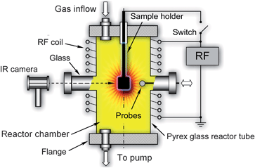 | ||
| Fig. 2 Schematic of a typical configuration of a simple plasma reactor that can used for the rapid, single-step, direct synthesis of metal oxide nanostructures. | ||
These amounts are determined by the oxygen gas pressure (total number of oxygen molecules available for dissociation), the dissociation rates, and the rates of losses of oxygen atoms (most importantly, due to recombination on solid surfaces). For instance, a flux of oxygen atoms of approximately ∼1.5 × 1024 (m2s)−1 is required to produce niobium pentoxide (Nb2O5) nanowires shown in Fig. 1(f).26 A somewhat lower flux of oxygen atoms (∼6 × 10²³ (m2s)−1) was used to synthesize Fe2O3 depicted in Fig. 1(c).28 The above fluxes of oxygen are quite high and care should be taken to maximize the dissociation rates of oxygen molecules on one hand, and minimize the recombination losses on the other one. This is why the walls of the reactor need to be made of a material with a low recombination probability of oxygen atoms on the surface. In the case of oxygen atoms recombination on Pyrex, the typical recombination rates are less than 0.01.12,28 On the other hand, the ICP discharge can be tailored to maximize the dissociation rates, and the dissociation degrees higher than 80% can be achieved.
More importantly, since the process is extremely sensitive to the flux of oxygen atoms (this flux determines the surface temperature and the rates of building material delivery to the localized nucleation areas) onto the growth surface, it is crucial to develop reliable diagnostic techniques for the real-time, in situ measurements of the densities of oxygen atoms. Among many plasma diagnostic techniques, only fiber optic catalytic probe (FOCP) approach appears to be the most accurate and reliable for this purpose.80,81 This technique is based on the precise measurements of the amounts of heat released through recombination of oxygen atoms on the outer surface of a hollow spherical ‘black body’ connected to an optical fibre. The black body emits EM radiation (in IR range) that is transmitted through the optical fibre to a suitable optoelectrical detector. The FOCP technique can unambiguously determine the number density of oxygen atoms in the plasma reactor (e.g., the post-glow area) with a reasonably high spatial resolution (∼ 1 mm). The FOC probes can be inserted through one of the diagnostic side arms/ports in the chamber as shown in Fig. 2. The lumped density of all (e.g., O+, O2+, O3+) positive oxygen ions nO+ can be estimated through the Langmuir Probe82 measurements. In charge-neutral plasmas this amount is matched by the combined densities of electrons ne and all negative ions nO−, hence, nO+ = ne + nO−. The combination of controlled production and measurement of densities of oxygen atoms ensures active process monitoring and control, which also involves in situ measurements of the surface temperature using infrared thermometry. An IR camera faces the substrate surface; these surface temperature measurements can be done through the IR-transparent window as shown in Fig. 2.
The plasma reactor described in this section was used to synthesize α-Fe2O3 and Nb2O5 nanowires depicted in Fig. 1(c) and 1(f). Several other plasma reactor configurations have been used to synthesize metal oxide and other inorganic nanostructures.2,3,8,31,33,53,57
5. SLS mechanism of nucleation and growth of oxide nanowires of easy-to-melt metals
In this section we will consider two examples of direct plasma-based synthesis of metal oxide nanostructures and focus on the SLS mechanism. The first example (Fig. 3) is related to β-Ga2O3 nanowires (see, e.g., Fig. 1(d))31 and the second one to CdO nanostructures (Fig. 4 and 5).9 In the first example (Fig. 3),31 gallium substrates are initially exposed to plasmas of pure hydrogen or H2 + O2 gas mixtures to produce relatively large areas (also commonly termed melt pools) of molten Ga. The plasma is produced in a commercial microwave plasma reactor ASTEX at working gas pressure of approximately 400 Torr. The amount of microwave power to sustain the microwave discharge at this pressure was ∼700 W. Under such conditions, the substrate temperature can reach 550 °C, which is well above the Ga melting point. Hydrogen and oxygen atoms are produced in the gas phase and then transported to the surface, where they recombine. The plasma also ionizes oxygen and hydrogen species. Heat released through the impact of ions and exothermic heterogeneous surface recombination of H and O atoms, leads to the formation of the Ga melt shown as a pink area in Fig. 3. Under very high surface temperatures due to the microwave plasma exposure, gallium melts over the entire surface of the sample.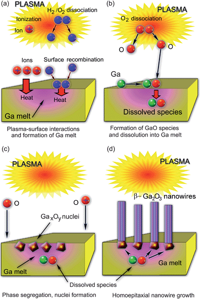
 | ||
| Fig. 4 Temporal dynamics of the surface temperature and three typical surface morphologies in the growth of CdO nanostructures in reactive oxygen plasmas. | ||
 | ||
| Fig. 5 Main growth stages of platelet-structured CdO nanopyramids formed on the surface of a Cd foil under a short exposure to reactive oxygen plasmas. | ||
During the second stage (Fig. 3(b)), hydrogen inlet is discontinued and only oxygen molecules are dissociated in the gas phase. Gallium oxide species are then formed on the surface of the melt and then ‘sink’ (dissolve) into the Ga melt. This process has two very interesting features: i) gallium melt is formed over large areas; ii) GaxOy nanophase nucleates and segregates near the interface between the Ga melt and the plasma (Fig. 3(c)). It is worthwhile to emphasize that the phase segregation leads to the formation of well-separated GaxOy nuclei rather than continuous GaxOy films. This makes the Ga-based process quite different as compared to the CdO nanopyramid case considered below. Thereafter, the as-nucleated GaO nanoparticles act as ‘bases’ for homoepitaxial growth of one-dimensional, single-crystalline β-Ga2O3 nanowires. The growth proceeds from the bottom using the species dissolved in the Ga melt (Fig. 3(d)).
It is important to mention that the process described in this section required a significant dilution of oxygen in hydrogen (flow rates of O2 in 100 sccm of H2 typically ranged from 0.6 to 10 sccm). According to Sharma and Sunkara,31 hydrogen (mostly atomic H produced by dissociation of H2 molecules in the plasma) is responsible for enhancing the nanowire growth by etching surface-segregated solid gallium oxide nuclei. This etching process significantly inhibits the lateral growth of surface nuclei by agglomeration. Noteworthy, dilution of precursor gases in hydrogen is frequently used in the growth of one-dimensional nanostructures of other materials systems (e.g., carbon/silicon nanotubes/nanotips). In the latter cases, atomic hydrogen forms hydrides with the main building atoms (e.g., carbon or silicon), which in turn leads in the significant reduction of the amount of unorganized (e.g., non-structured amorphous) material on the surface thus enhancing the growth of the desired one-dimensional nano-phase.6,7
A very exciting implication of the ‘free-floating’ GaO nuclei is the possibility to form a variety of nanostructures such as hollow tubes, solid straight (cylindrical and faceted) nanowires, and branched nanowires.31 For example, when each individual nucleus produces a nanowire, the nanowires are thin and their shape is usually cylindrical. If the nuclei agglomerate to form a ring, the emerging structures resemble thick hollow tubes. If the nuclei agglomerate to form a solid two-dimensional disk, solid faceted nanowires usually emerge. However, if the one-dimensional growth prevails at the beginning and is then affected by basal agglomeration, branched structures can eventually form.
Interestingly, the agglomeration of the initial nuclei can be reasonably controlled to obtain the nanostructures with the desired morphology and density.31 Each of the reported specific morphologies (nanowires, tubes, thick rods, and nanopaintbrushes) appeared under quite different process parameters, which in turn led to quite different conditions for the nucleation and agglomeration of the nanometre-sized nuclei in different substrate locations. For example, micrometre-scale tubular structures and nanopaintbrushes appeared near edges of the substrate and usually required higher oxygen flow rates and higher microwave powers. The nanoscale wires were observed near the center of the substrate on top of micrometre- to millimetre-sized Ga droplets. Furthermore, the well-faceted micron-sized rods clustered around the droplets of quite similar size. The oxygen flow rates, microwave power, operating pressure, and the process duration were quite similar in the last two cases. For the summary of the process conditions versus the morphological appearance of the resulting one-dimensional structures the reader can be referred to Table 1 of the original report.31
Another distinctive feature of this approach is that it usually produces a very high nucleation density of nanowires, which can even be greater than 1011 cm−2. However, this density is even higher than a typical density (∼1010 cm−2) of quantum dots (e.g., Ge on Si dots that are formed via Stranski–Krashtanov fragmentation) on the surface.83 This very high density of nucleation centers is very difficult, if possible at all, to control. This issue may become very significant in applications (e.g., energy conversion) that require a significant reduction of the nanostructure density.
The density of the resulting nanowire nuclei can be estimated by using a thermodynamic stability analysis.41 This analysis allows one to determine the levels of supersaturation of the solute (oxygen species in our case) in the solvent (Ga melt) at which the supersaturated melts segregate into liquid (Ga) and solid (β-Ga2O3) phases. The solid phase gives rise to the nanowire nuclei which in turn support the nanowire growth (Fig. 3). The model was successfully applied for the (plasma- or thermal-assisted) nucleation and growth of Ge nanowires from Ga melt and is applicable for one-dimensional structures of a variety of solid materials produced from melts of easy-to-melt metals such as Ga, In, or Sn (see Fig. 1(b) for high-density Bi nanowires produced using small Ga particles).41 However, this model cannot be directly applied for the β-Ga2O3 nanowires of our interest because the solute and solvent do not separate completely and form a β-Ga2O3 nanophase through bonding of oxygen and gallium atoms. Another complication arises from the fact that the solute in fact contains several oxygen species (e.g., O, O2, etc.). This creates excellent opportunities for the further development of theoretical approaches for nanowire nucleation and growth.
Another issue is a very long time required to grow the β-Ga2O3 nanowires; the growth process typically lasts from 1 to 12 h.31 A relatively faster process (also using a pool of molten Ga) was reported for the synthesis of α-SixOy straight and coiled nanowires.2,33 This process usually takes from 15 mins to 3 h; however, the nanowires produced are amorphous.
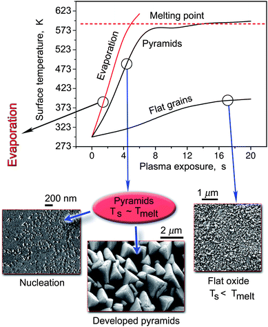
A much faster growth process of oxide nanostructures based on easy-to-melt metals which develop through the SLS mechanism9 is shown in Fig. 4 and 5. Even though this case was used as an example in Sec. 2 and 3 to introduce our deterministic approach, in this section we will present more specific details and comment on the sequence of phenomena that take place during the synthesis. We stress that the whole process of CdO nanostructure formation takes only 10–30 s. However, it appears to be very sensitive to the flux of oxygen atoms (which in turn determines the surface temperature) to the Cd surface. The three cases presented in Fig. 4 correspond to different densities of oxygen atoms and ions. It was found that when the density of ions is very low (ni <1015 m−3), and the density of oxygen atoms does not exceed ∼1.6 × 10²¹ m−3, only flat oxide grains are formed. In this case the surface temperature never reaches the melting point of Cd as can be seen from Fig. 4. In another extreme, when the density of oxygen atoms exceeds ∼3 × 10²¹ m−3, and ni > 3.5 × 10¹⁶ m−3, the surface temperature very quickly (within ∼ 5 s) overshoots the melting point of cadmium. A continued plasma exposure may lead to the complete evaporation of the Cd foil used in the experiments.
In a sense, the case when CdO nanostructures are formed is unique, since this is only possible when the dose of oxygen atoms Θ impinging on the surface varies from ∼1.5 to 9 × 1024 (m2s)−1. The lower is the dose of oxygen atoms, the smaller is the size of CdO pyramids. Indeed, it varies from less than 100 nm at the lower boundary of the oxygen atom dose to almost 2 μm at Θ ∼ 9 × 1024 (m2s)−1. The large developed CdO pyramids depicted in Fig. 4 correspond to Θ ∼ 7.3 × 1024 (m2s)−1. In this case the ion density is more than one order of magnitude higher than in the flat oxide case. This suggests that ion bombardment also plays a very significant role in the formation of this sort of nanostructures. The increased size of the nanostructures with the dose of oxygen atoms suggests that the sizes of the localized Cd melts also increase both with the time into the process and with the dose of oxygen atoms used. This important fact should also complement the basic nucleation and growth mechanism outlined in Secs. 2 and 3; a quite similar argument will also be used in explaining the VSS nucleation and growth of α-Fe2O3 nanowires of Sec. 6.
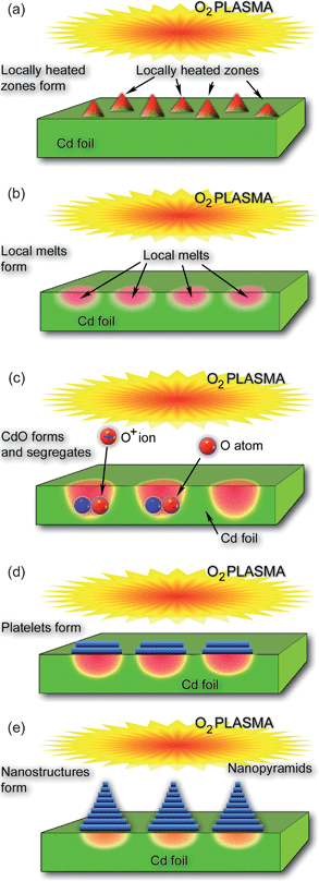
The sequence of phenomena that take place in the SLS nucleation and growth of CdO nano-pyramids is sketched in Fig. 5. This figure summarizes the ideas already discussed in this article; this is why we will only briefly comment on the main processes sketched in Fig. 5(a)-(e). When the surface of a Cd foil is exposed to O2 plasmas, localized heated zones (Fig. 5(a)) are formed in the areas where ion impact is particularly strong (here we recall that the ion flux increases dramatically under conditions when the nanopyramids are formed). As a result, cadmium material melts giving rise to local melts as shown in Fig. 5(b). Oxygen atoms and ions enter these molten areas and form CdO (Fig. 5(c)). Interestingly, segregation of CdO nanophase takes place under locally strained conditions which lead to the formation of the first CdO platelet at the interface between the cadmium melt and the plasma sheath (Fig. 5(d)). Subsequent platelets nucleate at the interface between the Cd melt and the developing CdO structure; this gives rise to the platelet-structured nanopyramids (Fig. 5(d), see also Fig. 4). It is noteworthy that the sizes of the local Cd melts strongly depend on the exposure to oxygen plasma, and more specifically, to the dose of oxygen atoms/ions interacting with the surface. This explains the reported clear (yet nonlinear) dependence of the average nanopyramid size on Θ (see the discussion above).
More importantly, the possibility to create localized ‘hot spots’ and eventually nanoscale melts on the surface of a Cd foil bring about two striking differences compared to the GaO nanowire case discussed above. First, the ‘localized’ nucleation of CdO under strained conditions made it possible to create basal plates and eventually the developed pyramids in the same localized areas. This is very different from the GaO case where the nanowire nuclei formation took place randomly over the entire area of molten gallium film (Fig. 3). On the other hand, self-organization of the floating and movable GaO nuclei led to the possibility of creation of a large variety of GaO nanostructures with different morphologies.31 This is quite different from exclusively pyramidal morphologies observed in the CdO case.9 Another striking difference between the two cases is in the typical duration of the growth process, which was only a couple of tens of seconds in the CdO case and several hours in the GaO case. Finally, CdO nanostructures were produced in one single step, while the synthesis of GaO nanowires required creation of a molten Ga layer on a substrate (e.g., quartz, sapphire, graphite, glassy carbon, etc.) prior to the nanowire synthesis.
The latter fact gives a clear indication that the ability to activate localized spots in the specified areas may be one of the most essential requirements for the direct, single-step growth of single-crystalline metal oxide nanostructures. As follows from the next two sections, localized nanoscale plasma-surface interactions also enable highly-controllable synthesis of single-crystalline nanowires of oxides of metals with high melting temperatures via the VSS growth mechanism.
6. VSS mechanism of nucleation and growth of Fe2O3 nanowires
When a solid material has a high melting temperature, which is above typical temperatures achievable through the exposure to low-pressure, thermally non-equilibrium plasmas, a different strategy should be used. Of course, one could use some other types of plasma discharges that can generate transiently high temperatures such as pulsed sparks.84 However, such exposure is very likely to lead to uncontrollable substrate heating, with poor surface area selectivity. Let us consider how one can create similarly activated, yet not fully molten, localized spots using the same approach as in Sec. 5. To understand how it may work, we will use a conventional iron-oxygen phase diagram (Fig. 6) and a sketch of a typical VSS nanowire growth process (Fig. 7).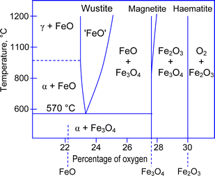
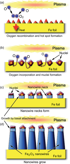
Let us start from a small nano-hillock on the surface (Fig. 7(a)). It is very clear that a nanowire can nucleate in some specific area only if some material property will change only in that specific area. In the SLS mechanism considered above, this change was related to the solid-to-liquid phase transition. If the solid has a high melting point (e.g., 1535 °C for iron), it is very difficult to implement. However, due to very small sizes of the nanoscale surface features, these solid-to-liquid phase transitions can take place close to the tip of the hillock (Fig. 7(a)), which is always hotter due to the effects of ion bombardment (as well as somewhat higher rates of oxygen recombination); moreover, a smaller size of the tip (compared to the base of the hillock) leads to much lower melting points.
In addition, any other materials phase may in principle be used to trigger the nanowire nucleation process. For instance, if a solid material has two thermodynamically stable phases, then one of the phases may nucleate within another phase, thus forming a segregated nanophase.86 This segregated nanophase may in turn serve as nanowire nuclei, very similar to the GaO case of Sec. 5. This exciting possibility becomes evident from the iron-oxygen phase diagram in Fig. 6. From this figure one can immediately notice that different iron oxide phases can co-exist near the 570 °C point. Hence, by increasing the temperature (through the oxygen plasma exposure similar to the case considered in the Sec. 5) to only slightly above this point, one can trigger phase transitions between iron oxide phases. In addition, this temperature may be sufficient for the localized melting of Fe near the nano-hillock tips. Moreover, intense oxygenation under plasma exposure may also increase the oxygen percentage in the nucleation areas, thus giving rise to preferential nucleation of the α-Fe2O3 phase. This iron oxide phase was most commonly observed in the iron oxide nanowires produced via the single-step direct plasma exposure.24 The varied oxygen content during the nucleation and growth may be the main reason for the initial instability observed during the initial growth stages of the nanowires.28
Fig. 7 shows the sequence of events that take place during the exposure of an iron surface to reactive oxygen plasmas. Localized activation of the ‘hot spots’ through the plasma-related heating (Fig. 7(a)) leads to the incorporation of oxygen atoms followed by the phase-transition-mediated formation of iron oxide nuclei as sketched in Fig. 7(b). Presumably, platelet structures also form in the VSS growth. A fine single-crystalline structure with crystalline planes which are usually parallel to the growth surface24 is an indication of the validity of this assumption. It was reported24,28 that during the transition from initial nucleation to the steady nanowire growth, the structure of the wire also changes. Indeed, a different structure was observed for the nanowire ‘necks’ (Fig. 7(c)) compared to the mature body of the developed α-Fe2O3 nanowires (Fig. 7(d)), which was attributed to the transient growth instability during the initial stage.28 The relatively small tapering of the nanowires indicates that interfacial tensile stress (presumably due to the presence of different phases in small localized areas) is a significant factor in the growth process, which is quite similar to the SLS mechanism of the previous section. It was also demonstrated that by applying a bias to the Fe substrate, one can control the aspect ratio, shape, and nucleation density of the α-Fe2O3 nanowires.16 In particular, when the localized nucleation spots are small and ions predominantly land closer to the tips of the developing nanostructures, very sharp nano-needles are formed. On the other hand, when the density of microscopic ion fluxes is also high near the nanowire bases, the hot spots widen; in this case thicker and longer nanowires form.16
The ratio of densities of the plasma-generated neutral oxygen atoms and O+ ions significantly affects the density and morphology of the α-Fe2O3 nanostructures. Indeed, when the relative density of O+ ions increases with respect to the density of neutral O atoms, the density and the aspect ratio of the nanowires also increase. These conclusions are based on the analysis of the results in the original report12 and are consistent with the available explanations of the possible roles of the plasma ions on the growth of one-dimensional nanostructures.87,88
It is worth emphasizing that the growth rates of metal oxide nanowires grown via the VSS mechanism are very high and are comparable to the SLS growth. Experiments with α-Fe2O3, Nb2O5, CuO2 and V2O5 demonstrated that it typically takes only 1–3 min to synthesize the fully-developed nanowire array. Atmospheric pressure plasmas and hot-filament systems have also been successfully used for the synthesis of large amounts of WO2/WO3, Ta2O5, and NiO nanowires.44
For most of the cases when the growth is reasonably slow to detect the difference (e.g., iron oxide and niobium oxide nanowires), the growth rates experience a strong increase (rapid growth stage) after the initial nucleation stage followed by the slower growth at the later stage. This conclusion was made by comparing the lengths of the nanowires grown in processes of different durations. This is consistent with the results of other authors on the growth of one-dimensional nanostructures.7,8,10,78,88,89 For the short-duration processes (e.g., synthesis of CdO nanostructures which typically takes only a few to a few tens of seconds,9 see also Sec. 5), this conclusion is very challenging to verify because excessively long plasma exposure times lead to the major overlap of the individual nanostructures and hence, the significant deterioration of the resulting micropattern. The surface temperature and the oxygen dose are closely related. Indeed, higher oxygen doses result in higher surface temperatures due to increased surface recombination and the consequent release of energy.12,16 Within the ranges of possible nanostructure formation, the growth rates increase with the oxygen dose (and hence, with the surface temperature); this dependence is non-linear (growth slows down when the oxygen dose/temperature increase) and is consistent with the established views of thin film/nanostructure growth (see, e.g.2,3,6,7 and references therein).
We also stress that under the same process time and oxygen dose, higher surface roughness leads to higher densities of nanowires (e.g., Fe/Nb oxide). The nanowires grown on the surfaces with higher roughness also often appear thicker; there is no direct relation between the surface roughness and the final aspect ratio, which is most effectively controlled by the process time and oxygen dose as well as other plasma parameters such as the ion density/flux and energy.
Another common feature of the plasma-based processes (discussed in Secs. 5 and 6) of our interest is that the role of ion bombardment becomes even more significant after the nucleation stage. As the nanowires develop, their aspect ratios increase. This in turn leads to stronger focusing of the plasma ions near the tips.88 The tips in many cases appear somewhat flattened, which presumably happens because of the ion impacts and the associated sputtering effects.18,20,22 Interestingly, a quite similar effect has previously been reported for single-crystalline carbon nanotip structures.90
We emphasize that despite the significant advances in the synthesis and applications of the metal oxide nanowires synthesized via the VSS mechanism, the understanding of the nucleation and growth processes in oxygen plasmas still remains essentially incomplete.2,3 For example, the role of surface adatom/adradical diffusion processes that drive the growth of many self-organized nanostructures it is not completely clear. Indeed, in the platelet-based growth mechanism discussed in this and previous sections, the platelets most likely nucleate upon incorporation of oxygen atoms in the (molten) liquid or (activated) solid phase near the top surface of the metal exposed to oxygen plasmas. At this stage, the growth proceeds by nucleation of new platelets (single layers of bonded metal and oxygen atoms).
However, one should bear in mind that this nucleation may take place both under the bottom-most existing platelet by combination of dissolved oxygen atoms in the (molten) liquid or (activated) solid phase near the top surface of the metal as well as on top of the top-most platelet of the growing nanowire. Both routes are thermodynamically possible, yet have quite different probabilities under specific process conditions. Indeed, for the first process to take place metal atoms are already in place and a large number of dissolved oxygen atoms are available for bonding. On the other hand, the second process requires metal atoms to escape (e.g., evaporate) the surface of the metal foil and then redeposit onto the surface and then diffuse onto the top of the top-most platelet where they may combine with incoming oxygen atoms and ions to eventually nucleate as a new platelet. As the nanowire grows longer, the probability of metal atoms to reach the existing top platelet decreases significantly, so does the relative importance of the metal atom evaporation/diffusion-based mechanism (this conclusion is based on the analysis of a similar case of the plasma-based growth of carbon nanostructures89). Furthermore, the surface temperatures typically used in the growth experiments are much lower than the sublimation temperatures; this is why we believe that the contribution of the metal evaporation-based process should be relatively small. To verify these possibilities, a dedicated study is required. However, it is clear that the surface diffusion of metal atoms to the tip of nanowires may be a contributor to the nanowire growth process. Further, metal oxide molecules, or even clusters might be formed in the gas phase by the evaporation from the melt or the activated metal surface may also contribute to the nanostructure growth process. Therefore, detailed studies of the relative contributions of different species and growth channels are required.
From the above, one can conclude that the plasma-assisted VSS growth of metal oxide nanowires is an exciting area full of interesting phenomena that are not yet properly understood. The following section is devoted to numerical simulations related to the plasma-specific effects on the nucleation and growth of iron oxide nanowires in oxygen plasmas.
7. Numerical simulations
Our previous simulations16 have demonstrated the correlations between the plasma process conditions (e.g., ion/radical density, substrate bias) and the morphology of the Fe2O3 nanowire patterns. Having failed to produce SiO2 nanowires via the direct exposure of Si sample to oxygen plasmas, we have nevertheless demonstrated the possibility of the controlled formation of small SiO2 nanodots that develop intricate self-organized patterns depending on the process duration and the dose of oxygen atoms used.14 Numerical simulation has also revealed the possibility that the SiO2 dots preferentially form on nano-hillocks with the sizes above the ‘nucleation level’ mapped using atomic force microscopy (AFM). It was revealed that the initial stage of oxidation of the silicon surface with nano-hillocks may proceed via the localized nucleation mechanism contrary to the commonly accepted Deal-Grove mechanism which implies the formation of an ultra-thin oxide layer over the entire area of the smooth surface.Here we have performed a similar simulation which shows that the most probable nucleation sites can also be predicted for the VSS growth of iron oxide nanowires. In the simulation, we have used a random pattern of small surface features on otherwise atomically smooth Fe surface. The sizes of the hillocks were also related to the non-uniform two-dimensional (2D) temperature field, with higher temperatures near the tips (due to ion flux heating) and uniform temperature elsewhere. The density of oxygen atoms on the surface was simulated by using a two-dimensional (2D) diffusion model48 which makes it possible to compute 2D maps of adatom densities and fluxes over microscopic surface areas. This model incorporates the incoming and outgoing fluxes of oxygen atoms to and from the iron surface; these fluxes were calculated by using the experimental data for the oxygen fluxes and the typical recombination rates on the surface. Oxygen atoms were assumed to diffuse between the hillocks and incorporate into them at the dissolution/incorporation rates that were related to the nano-hillock sizes and the local temperature. A certain amount (nucleation threshold) of oxygen atoms incorporated in any particular hillock heralded the localized nucleation event. Typical parameters that were used in these simulations are: flux of oxygen atoms to the surface 6 × 10²³ (m2s)−1, surface recombination coefficient 0.09, surface temperature 585 °C, initial density of nano-hillocks (all larger than 2.5 nm in height but smaller than 15 nm; Gaussian distribution by sizes) 2 × 1010 cm−2; surface attachment (physisorption) and ‘evaporation’ (desorption) rates were temperature-dependent. The rates of oxygen adatom capture by the hillocks were determined by setting and updating the boundary conditions around every specific hillock. These conditions were determined by using the adatom density16,48 and flux86 approaches; in both approaches, reasonable ‘nucleation thresholds’ were set. Specifically, if a nano-hillock of a specific size captures the amount of oxygen atoms of approximately 1/2 to 2/3 of the number of iron atoms it contains (these numbers correspond to the probable formation of the Fe2O3 nanophase), the nucleation event was assumed to have happened. The number of the captured oxygen atoms was calculated using both approaches; the results from both approaches were reasonably close.
Fig. 8 visualizes the results of such simulations that allowed us to compute the 2D field of adatom density, and, in particular, in the areas of location of every specific hillock (boundary conditions were set and updated, after each time step, on each of them). The three arrows in Fig. 8 point on the small area where a non-nucleated (hidden in simulations) hillock is located and where the density/flux of oxygen adatoms is high enough to trigger the nucleation. This area is denoted as the area of the probable nucleation site of iron oxide nanostructures. These simulations allow one to predict, with a reasonably high level of physical accuracy, the localized areas where the nanostructure nucleation is likely to take place.
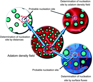 | ||
| Fig. 8 Nucleation of iron oxide nanowires visualized via multiscale hybrid numerical simulations. Two-dimensional fields of adatom densities and surface fluxes make it possible to determine the most probable morphological features of the surface where nanowire nucleation is most likely. | ||
Fig. 9 visualizes the mechanisms taken into account in the simulation of the growth and reshaping of iron oxide nanowires at more advanced growth stages but at the same parameters as in Fig. 8. These simulations are based on Monte-Carlo simulations of ion trajectories in the electric fields in the plasma sheath and in the vicinity of the nanowires, combined with the 2D simulation of adatom density/flux fields similar to Fig. 8. More details about similar simulations/modelling can be found in our previous publications.88,91Fig. 9 shows the distributions of microscopic ion currents in the spaces between the nanowires as well as along the nanowire length. These distributions are complemented with the 2D fields of ion currents (Fig. 9(a), see also a histogram along the line connecting two nanowires), adatom density between the nanowires (Fig. 9(b)), and adatom fluxes to the nanowires. Because of the assumed basal attachment growth mechanism, the adatoms and adions that land on the nanowire lateral surfaces can only participate in the nanowire growth only if they can reach the localized hot spot area at the nanowire base. As the nanowires grow longer, the contribution of these species becomes smaller. A similar phenomenon significantly affects the growth rates of carbon nanotubes, nanofibers, and other 1D nanostructures.55,91,92
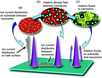 | ||
| Fig. 9 Three-dimensional topographies of microscopic ion fluxes, adatom density fields, and adatom fluxes in the arrays of growing nanowires make it possible to compute the nanowire shapes and growth rates at advanced growth stages. | ||
At this stage, these multiscale simulations do not account for many specific details of plasma-surface interactions. For example, these simulations should be complemented by detailed modeling of the reactive oxygen plasma chemistry and will also require a more rigorous treatment of interactions of numerous oxygen species with the nanostructures and open surface areas between the nanostructures. However, each of the model refinements comes at a huge computational cost and a number of simplifying physical assumptions have to be made. For a concise summary of space/time scales and the physical assumptions used in the simulation of the growth of one-dimensional nanostructures the reader can be referred elsewhere.89
8. Conclusion
In this article we have attempted to perform the detailed analysis of many interesting physical phenomena involved in the nucleation and growth of metal oxide nanostructures in the rapid, single-step, direct synthesis which is based on the exposure of a solid material to the reactive oxygen plasma. Even though the possibility of this nanowire synthesis approach was discovered in 2005,18 it has already been applied to a reasonably broad number of materials systems. Since then, the team of authors and many other researchers spent significant efforts to understand how exactly this approach works, and in particular, what are the specific roles of the reactive plasma environment. To some extent, this article is a summary of our extensive experience of work in the area of plasma nanoscience, which specifically aims to elucidate the roles of the plasma environment in nanoscale synthesis.6,45 Most importantly, the process examined in this work is impossible without the plasma exposure; similar thermal (e.g., reactive vapor transport, chemical vapor deposition, etc.) processes lead to very different outcomes and also take significantly longer time.The plasma-based approach advocated in this article, leads to very fast, energy-efficient, and environmentally benign synthesis of a variety of metal oxide nanostructures, which in turn find numerous applications in energy conversion, electrochemistry, sensing, water splitting and sterilization, and many other areas. This is why we believe this approach can be scaled up to become suitable for large-scale industrial production of surface-supported metal oxide nanowires.
We hope that after reading this article, the reader will get the impression that the single-step nanowire synthesis process based on our ‘deterministic’ strategy (which in fact we kept developing in the last 5–6 years, via a series of endless experiments and numerical modeling) is pre-determined and is really an ‘easy magic’ (and then possibly will try this approach in their own lab). Moreover, we believe that presenting the knowledge that became available to us through the course of the work with the nanowires and the plasma nanoscience in a pre-determined, ‘deterministic’ way will be very useful for other researchers in the development of plasma-based nanoscale synthesis approaches and significantly shorten the experimental trials.
The knowledge presented in this article still lacks understanding of many important phenomena, such as what happens during the initial nucleation stages. This creates exciting opportunities for multidisciplinary collaborations. Finally, we believe that more and more researchers will adopt plasma-based nanotools in their labs and will harness numerous benefits of using low-temperature plasmas in nanoscale synthesis and processing.
Acknowledgements
This work is partially supported by the Australian Research Council, CSIRO's Science Leadership Program (Australia), Slovenian Research Agency (ARRS), National Science Foundation, and Department of Energy (USA). The authors thank many of our collaborators and team members, especially S. Vaddiraju, S. Sharma, Z. Chen, G. Bhimarasetti, A. Drenik, I. Junkar, and A. D. Arulsamy for their contributions to this research area, fruitful discussions and technical assistance.References
- W. Lu and C. M. Lieber, J. Phys. D: Appl. Phys., 2006, 39, R387 CrossRef CAS.
- M. Meyyappan and M. K. Sunkara, Inorganic Nanowires: Applications, Properties and Characterization, CRC Press, New York, 2010 Search PubMed.
- J. Zheng, R. Yang, L. Xie, J. Qu, Y. Liu and X. Li, Adv. Mater., 2010, 22, 1451 CrossRef CAS.
- X. L. Wang and V. Voliotis, J. Appl. Phys., 2006, 99, 121301 CrossRef.
- W.-H. Chiang and R. M. Sankaran, Nat. Mater., 2009, 8, 882 CrossRef.
- K. Ostrikov, Rev. Mod. Phys., 2005, 77, 489 CrossRef CAS.
- M. Meyyappan, J. Phys. D: Appl. Phys., 2009, 42, 213001 CrossRef.
- A. Borras, A. Barranco, J. P. Espinos, J. Cotrino, J. P. Holgado and A. R. Gonzalez-Elipe, Plasma Processes Polym., 2007, 4, 515 Search PubMed.
- U. Cvelbar, K. Ostrikov and M. Mozetic, Nanotechnology, 2008, 19, 405605 CrossRef.
- P. J. Alet, L. Yu, G. Patriarche, S. Palacina and P. Roca i. Cabarrocas, J. Mater. Chem., 2008, 18, 5187 RSC.
- J. Shieh, F. J. Hou, Y. C. Chen, H. M. Chen, S. P. Yang, C. C. Cheng and H. L. Chen, Adv. Mater., 2010, 22, 597 CrossRef CAS.
- U. Cvelbar and K. Ostrikov, Cryst. Growth Des., 2008, 8, 4347 CrossRef CAS.
- L. F. Cui, Y. Yang, C. M. Hsu and Y. Cui, Nano Lett., 2009, 9, 3370 CrossRef CAS.
- I. Levchenko, U. Cvelbar and K. Ostrikov, Appl. Phys. Lett., 2009, 95, 021502 CrossRef.
- Z. Dong, P. Kashkarov and H. Zhang, Nanoscale, 2010, 2, 524 RSC.
- U. Cvelbar, K. Ostrikov, I. Levchenko, M. Mozetic and M. K. Sunkara, Appl. Phys. Lett., 2009, 94, 211502 CrossRef.
- F. J. Gordillo-Vázquez, V. J. Herrero and I. Tanarro, Chem. Vap. Deposition, 2007, 13, 267 CrossRef CAS.
- M. Mozetič, U. Cvelbar, M. K. Sunkara and S. Vaddiraju, Adv. Mater., 2005, 17, 2138 CrossRef CAS.
- Y. P. Hsieh, H. Y. Chen, M. Z. Lin, S. C. Shiu, M. Hofmann, M. Y. Chern, X. Jia, Y. J. Yang, H. J. Chang, H. M. Huang, S. C. Tseng, L. C. Chen, K. H. Chen, C. F. Lin, X. C. T. Liang and Y. F. Chen, Nano Lett., 2009, 9, 1839 CrossRef CAS.
- U. Cvelbar, K. Ostrikov, A. Drenik and M. Mozetic, Appl. Phys. Lett., 2008, 92, 133505 CrossRef.
- C. H. Hsu, H. C. Lo, C. F. Chen, C. T. Wu, J. S. Hwang, D. Das, J. Tsai, L. C. Chen and K. H. Chen, Nano Lett., 2004, 4, 471 CrossRef CAS.
- A. Drenik, U. Cvelbar, K. Ostrikov and M. Mozetic, J. Phys. D: Appl. Phys., 2008, 41, 115201 CrossRef.
- A. Fontcuberta i Morral, J. Arbiol, J. D. Prades, A. Cirera and J. R. Morante, Adv. Mater., 2007, 19, 1347 CrossRef CAS.
- Z. Chen, U. Cvelbar, M. Mozetic, J. He and M. K. Sunkara, Chem. Mater., 2008, 20, 3224 CrossRef CAS.
- S. Kodambaka, J. Tersoff, M. C. Reuter and F. M. Ross, Science, 2007, 316, 729 CrossRef CAS.
- U. Cvelbar and M. Mozetic, J. Phys. D: Appl. Phys., 2007, 40, 2300 CrossRef CAS.
- T. Y. Zhai, X. S. Fang, L. Li and D. Golberg, Nanoscale, 2010, 2, 168 RSC.
- U. Cvelbar, Z. Q. Chen, M. K. Sunkara and M. Mozetič, Small, 2008, 4, 1610 CrossRef CAS.
- M. Yang, G. S. Pang, L. F. Jiang and S. H. Feng, Nanotechnology, 2006, 17, 206 CrossRef CAS.
- K. Keem, H. Kim, G. T. Kim, J. S. Lee, B. Min, K. Cho, M. Y. Sung and S. Kim, Appl. Phys. Lett., 2004, 84, 4376 CrossRef CAS.
- S. Sharma and M. K. Sunkara, J. Am. Chem. Soc., 2002, 124, 12288 CrossRef CAS.
- Ü. Özgür, Y. I. Alivov, C. Liu, A. Teke, M. A. Reshchikov, S. Doğan, V. Avrutin, S. I. Cho and H. Morkoç, J. Appl. Phys., 2005, 98, 041301 CrossRef.
- M. K. Sunkara, S. Sharma, H. Chandrasekaran, M. Talbott, K. Krogman and G. Bhimarsetti, J. Mater. Chem., 2004, 14, 590 RSC.
- U. M. Graham, S. Sharma, M. K. Sunkara and B. H. Davis, Adv. Funct. Mater., 2003, 13, 576 CrossRef CAS.
- Z. J. Gu, F. Liu, J. Y. Howe, M. P. Paranthaman and Z. W. Pan, Nanoscale, 2009, 1, 347 RSC.
- J. Thangala, Z. Chen, A. Chin, C.-Z. Ning and M. K. Sunkara, Cryst. Growth Des., 2009, 9, 3177 CrossRef CAS.
- S. W. Kim, S. Fujita and S. Fujita, Appl. Phys. Lett., 2005, 86, 153119 CrossRef.
- V. Chakrapani, J. Thangala and M. K. Sunkara, Int. J. Hydrogen Energy, 2009, 34, 9050 CrossRef CAS.
- M. S. Arnold, P. Avouris, Z. W. Pan and Z. L. Wang, J. Phys. Chem. B, 2003, 107, 659 CrossRef CAS.
- P. Meduri, C. Pendyala, V. Kumar, G. U. Sumanasekera and M. K. Sunkara, Nano Lett., 2009, 9, 612 CrossRef CAS.
- H. Chandrasekaran, G. U. Sumanasekera and M. K. Sunkara, J. Phys. Chem. B, 2006, 110, 18351 CrossRef CAS.
- S. Gubbala, V. Chakrapani, V. Kumar and M. K. Sunkara, Adv. Funct. Mater., 2008, 18, 2411 CrossRef CAS.
- C. H. Liu, J. A. Zapien, Y. Yao, X. M. Meng, C. S. Lee, S. S. Fan, Y. Lifshitz and S. T. Lee, Adv. Mater., 2003, 15, 838 CrossRef CAS.
- J. Thangala, S. Vaddiraju, R. Bogale, R. Thurman, T. Powers, B. Deb and M. K. Sunkara, Small, 2007, 3, 890 CrossRef CAS.
- K. Ostrikov and A. B. Murphy, J. Phys. D: Appl. Phys., 2007, 40, 2223 CrossRef CAS.
- J. Y. Son, S. J. Lim, J. H. Cho, W. K. Seong and H. Kim, Appl. Phys. Lett., 2008, 93, 053109 CrossRef.
- Q. Wan, Q. H. Li, Y. J. Chen, T. H. Wang, X. L. He, J. P. Li and C. L. Lin, Appl. Phys. Lett., 2004, 84, 3654 CrossRef CAS.
- I. Levchenko, K. Ostrikov and D. Mariotti, Carbon, 2009, 47, 344 CrossRef CAS.
- H. T. Wang, B. S. Kang, F. Ren, L. C. Tien, P. W. Sadik, D. P. Norton, S. J. Pearton and J. Lin, Appl. Phys. Lett., 2005, 86, 243503 CrossRef.
- J. Y. Park, Y. S. Yun, Y. S. Hong, H. Oh, J. J. Kim and S. S. Kim, Appl. Phys. Lett., 2005, 87, 123108 CrossRef.
- I. Levchenko, K. Ostrikov and S. Xu, J. Phys. D: Appl. Phys., 2009, 42, 125207 CrossRef.
- Z. W. Pan, S. Dai, C. M. Rouleau and D. H. Lowndes, Angew. Chem., Int. Ed., 2005, 44, 274 CrossRef CAS.
- D. Mariotti, A. C. Bose and K. Ostrikov, IEEE Trans. Plasma Sci., 2009, 37, 1027 CrossRef CAS.
- D. N. Tafen and J. P. Lewis, Phys. Rev. B: Condens. Matter Mater. Phys., 2009, 80, 014104 CrossRef.
- M. Keidar, I. Levchenko, T. Arbel, M. Alexander, A. M. Waas and K. Ostrikov, Appl. Phys. Lett., 2008, 92, 043129 CrossRef.
- Q. H. Li, Y. X. Liang, Q. Wan and T. H. Wang, Appl. Phys. Lett., 2004, 85, 6389 CrossRef.
- D. Mariotti, H. Lindstrom, A. C. Bose, K. Ostrikov and T. Sasaki, Nanotechnology, 2008, 19, 495302 CrossRef.
- H. Kind, H. Q. Yan, B. Messer, M. Law and P. Yang, Adv. Mater., 2002, 14, 158 CrossRef CAS.
- S. Y. Huang, K. Ostrikov and S. Xu, J. Appl. Phys., 2008, 104, 033301 CrossRef.
- W. I. Park and G. Yi, Adv. Mater., 2004, 16, 87 CrossRef CAS.
- Z. Y. Fan and J. G. Lu, Appl. Phys. Lett., 2005, 86, 123510 CrossRef.
- D. Mariotti and K. Ostrikov, J. Phys. D: Appl. Phys., 2009, 42, 092002 CrossRef.
- Y. Li, G. W. Meng, L. D. Zhang and F. Phillipp, Appl. Phys. Lett., 2000, 76, 2011 CrossRef CAS.
- C. Q. Sun, Prog. Mater. Sci., 2009, 54, 179 CrossRef CAS.
- C. Q. Sun, Prog. Solid State Chem., 2007, 35, 1 CrossRef CAS.
- G. J. Zhang, L. Zhang, M. J. Huang, Z. H. H. Luo, G. K. I. Tay, E. J. A. Lim, T. G. Kang, G. Tae and Y. Chen, Sens. Actuators, B, 2010, 146, 138 CrossRef.
- M. H. Lee, D. H. Lee, S. W. Jung, K. N. Lee, Y. S. Park and W. K. Seong, Nanomed.: Nanotechnol., Biol. Med., 2010, 6, 78 CrossRef CAS.
- H. J. Choi, H. K. Seong, J. Chang, K. I. Lee, Y. J. Park, J. J. Kim, S. K. Lee, R. R. He, T. Kuykendall and P. D. Yang, Adv. Mater., 2005, 17, 1351 CrossRef CAS.
- C. Buzea, I. I. Pacheco and K. Robbie, Biointerphases, 2007, 2, MR17.
- B. J. Kim, J. Tersoff, S. Kodambaka, M. C. Reuter, E. A. Stach and F. M. Ross, Science, 2008, 322, 1070 CrossRef CAS.
- I. Levchenko and K. Ostrikov, Appl. Phys. Lett., 2008, 92, 063108 CrossRef.
- A. R. Harutyunyan, G. Chen, T. M. Paronyan, E. M. Pigos, O. A. Kuznetsov, K. Hewaparakrama, S. M. Kim, D. Zakharov, E. A. Stach and G. U. Sumanasekera, Science, 2009, 326, 116 CrossRef CAS.
- V. Schmidt, J. V. Wittemann and U. Goesele, Chem. Rev., 2010, 110, 361 CrossRef CAS.
- G. Schierning, R. Theissmann, H. Wiggers, D. Sudfeld, A. Ebbers, D. Franke, V. T. Witusiewicz and M. Apel, J. Appl. Phys., 2008, 103, 084305 CrossRef.
- H. Zhang and D. Y. Wang, Angew. Chem., Int. Ed., 2008, 47, 3984 CrossRef CAS.
- K.-H. Müeller, J. Appl. Phys., 1985, 58, 2573 CrossRef CAS.
- S. Sriraman, S. Agrawal, E. S. Aydil and D. Maroudas, Nature, 2002, 418, 62 CrossRef CAS.
- I. B. Denysenko, S. Xu, P. P. Rutkevych, J. D. Long, N. A. Azarenkov and K. Ostrikov, J. Appl. Phys., 2004, 95, 2713 CrossRef CAS.
- K. N. Ostrikov, S. Xu and A. B. M. S. Azam, J. Vac. Sci. Technol., A, 2002, 20, 251 CrossRef CAS.
- M. Mozetič, A. Ricard, D. Babič, I. Poberaj, J. Levaton, V. Monna and U. Cvelbar, J. Vac. Sci. Technol., A, 2003, 21, 369 CrossRef CAS.
- M. Mozetic, U. Cvelbar, A. Vesel, A. Ricard, D. Babic and I. Poberaj, J. Appl. Phys., 2005, 97, 103308 CrossRef.
- S. Xu, K. N. Ostrikov, Y. Li, E. L. Tsakadze and I. R. Jones, Phys. Plasmas, 2001, 8, 2549 CrossRef CAS.
- I. Levchenko, K. Ostrikov and A. B. Murphy, J. Phys. D: Appl. Phys., 2008, 41, 092001 CrossRef.
- J. H. Byeon and J. W. Kim, Appl. Phys. Lett., 2010, 96, 153102 CrossRef.
- Handbook of Chemistry and Physics, ed D. R. Lide, CRC Press, New York, USA, 88th edn Search PubMed.
- G. Abrasonis, G. J. Kovacs, L. Ryves, M. Krause, A. Mucklich, F. Munnik, T. W. H. Oates, M. M. M. Bilek and W. Moller, J. Appl. Phys., 2009, 105, 083518 CrossRef.
- I. Levchenko and K. Ostrikov, Appl. Phys. Lett., 2009, 95, 243102 CrossRef.
- I. Levchenko and K. Ostrikov, J. Phys. D: Appl. Phys., 2007, 40, 2308 CrossRef CAS.
- E. Tam and K. Ostrikov, Nanotechnology, 2009, 20, 375603 CrossRef.
- I. Levchenko, K. Ostrikov, J. D. Long and S. Xu, Appl. Phys. Lett., 2007, 91, 113115 CrossRef.
- I. Denysenko and K. Ostrikov, Appl. Phys. Lett., 2007, 90, 251501 CrossRef.
- Z. L. Tsakadze, I. Levchenko, K. Ostrikov and S. Xu, Carbon, 2007, 45, 2022 CrossRef.
| This journal is © The Royal Society of Chemistry 2010 |