Additive nanoscale embedding of functional nanoparticles on silicon surface†
Massimiliano
Cavallini
*a,
Felice C.
Simeone
a,
Francesco
Borgatti
a,
Cristiano
Albonetti
a,
Vittorio
Morandi
b,
Claudio
Sangregorio
cd,
Claudia
Innocenti
d,
Francesco
Pineider
d,
Emilia
Annese
e,
Giancarlo
Panaccione
e and
Luca
Pasquali
f
aCNR-ISMN, Via P. Gobetti 101, I-40129, Bologna, Italy. E-mail: m.cavallini@bo.ismn.cnr.it
bCNR-IMM Bologna, Via P. Gobetti 101, I-4012, Bologna, Italy
cCNR-ISTM Milano, Via C. Golgi 19, I-20133, Milano, Italy
dINSTM and Dep. of Chemistry “ U. Schiff” Università di Firenze, Via della Lastruccia 3–13, 50019, Sesto Fiorentino (FI), Italy
eCNR-INFM-TASC S.S. 14-Km 163.5, AREA Science Park, I-34149, Basovizza (TS), Italy
fDep. of Materials and Environmental Engineering, University of Modena and Reggio Emilia, Via Vignolese 905, 41100, Modena, Italy
First published on 9th August 2010
Abstract
We present a novel additive process, which allows the spatially controlled integration of nanoparticles (NPs) inside silicon surfaces. The NPs are placed between a conductive stamp and a silicon surface; by applying a bias voltage a SiO2 layer grows underneath the stamp protrusions, thus embedding the particles. We report the successful nanoembedding of CoFe2O4 nanoparticles patterned in lines, grids and logic structures.
In recent years chemists have synthesized a very large variety of novel nanometric objects such as clusters,1,2 supramolecular systems3 and particles4,5 exhibiting exciting functionalities that could be applied to various technological fields such as electronics,6 catalysis,5 sensors,7 solar cells8 and high-density information storage.9 The nanometric size of these objects leads to new and enhanced functionalities, but their exploitation is often compromised by their poor integration in current production processes. Although this issue is most evident in some specific fields such as high-density information storage and micro/nano-electronics, the integration of nano-objects in devices is a common problem in nanotechnology.
Among the several methods and processes proposed for the integration of nano-objects in devices,10–13 the ones relying on the “embedding” of materials of interest are largely used for applications in optics,14,15 micro-mechanics16 and magnetism17,18 to better exploit the functionalities of nano-objects or to improve some physical properties of the matrix. In conventional embedding nano-objects are usually dispersed inside a protective environment established by a matrix which can either be organic or inorganic to exploit the properties of the individual objects, otherwise hampered by possible chemical instabilities or aggregation phenomena. Up to now, several different embedding procedures have been developed,10–13 but some unresolved issues still need to be addressed. In particular, no spatial control of dispersed nano-objects can be achieved unless embedding is combined with complex and expensive lithographic procedures.19
In this work we present a novel approach named nanoembedding (n-EM) which merges in a single process the advantages of a spatially controlled nanopatterning20 and the conventional embedding approach. We report here the successful nanoembedding of cobalt ferrite (CoFe2O4) nanoparticles with average diameter 6.0 ± 1.3 nm (see ESI†) on a silicon wafer. CoFe2O4 is a largely investigated material which, thanks to the large magnetic anisotropy,21 exhibits high blocking temperatures even for very low grain size. This property, jointly with its chemical stability, makes CoFe2O4 an appealing magnetic material for several applications such as high-density information storage, high performance small components (e.g. capacitors), anti-reflection coatings and catalysis.22 A scheme of the process is depicted in Fig. 1: the nano-objects are placed between the protrusions of a conductive stamp and a semiconductive surface in a vapor rich environment. By applying a bias voltage, the sample surface is oxidized, forming an oxide film that grows around the nano-objects. The process acts only under the stamp protrusions, therefore it does not require any lithographic manipulation of the nano-objects, which can be directly deposited either on the stamp or onto the surface (see ESI†).
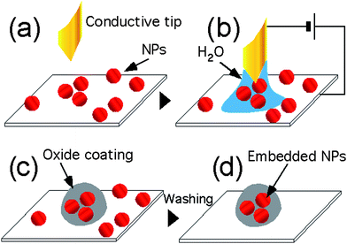 | ||
| Fig. 1 Scheme of nanoembedding. (a) NPs are deposited on the surface. (b) A conductive tip, or stamp protrusion, is placed in proximity of the NP in a vapour rich environment that forms a meniscus, after that a bias is applied, oxidizing the surface. (c) The NPs under the stamp protrusion are embedded into the oxide coating. (d) Non-embedded NPs are removed by washing the sample. | ||
The thickness of the capping oxide layer can be varied between 2 and 25 nm and depends on the bias voltage, application time, size of the nano-objects and the relative humidity (RH), similarly to the conventional local oxidation technique.23–25 Using 6 nm size CoFe2O4 NPs, 20 V bias applied for 10 s with RH 80% we obtained a SiOx thickness of 10 nm. After the n-EM procedure, the non-embedded objects can be easily removed by washing the sample surface with the same solvent used for NPs deposition (this step is not necessary if the NPs are deposited on the stamp).
The application of n-EM to real systems is shown in Fig. 2. Here the stamp motif consists of a series of parallel lines 200 nm wide with a 1.5 µm periodicity (Fig. 2a–d) and a logic pattern, i.e. a pattern containing information in binary code (Fig. 2e, see also ESI†).
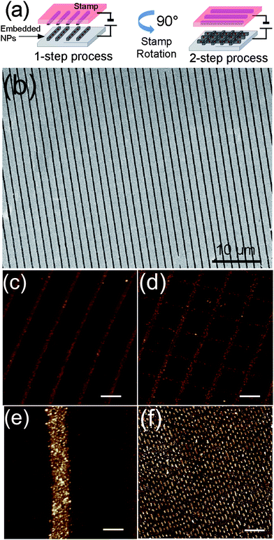 | ||
| Fig. 2 (a) Scheme of 2-step nanoembedding; (b) 60 × 40 µm2 SEM micrograph of CoFe2O4 NPs embedded on silicon oxide inside parallel stripes; (c) corresponding AFM (zoom) image; bar is 1 µm, Z scale 0–20 nm; (d) results of 2-step n-EM obtained from sample b after repeating the process rotating the same stamp by 90°; bar is 1 µm, Z scale 0–20 nm; (e) single stripe of CoFe2O4 NPs embedded at high density of NPs (∼300 NPs µm−2); bar is 200 nm, Z scale 0–20 nm; (f) demonstration of a logic pattern obtained from the replica of a digital video disk; bar is 3 µm, Z scale 0–25 nm. | ||
Fig. 2b and c show SEM and AFM images of parallel stripes containing a low density of NPs (∼75 NPs µm−2, measured from AFM image) while Fig. 2d shows the same sample in which n-EM has been performed twice, rotating the stamp 90° before the second application (2-step process). The images clearly show the repeatability of n-EM on the same sample and the possibility to obtain complex distributions by simply combining multiple applications additively.
The quantity of embedded NPs is controlled during their deposition on the stamp (or on the surface) controlling the concentration of the initial solution. As an example, Fig. 2e shows the detail of a single stripe obtained using a higher density of NPs (∼300 NPs µm2 measured from AFM images). Finally, Fig. 2f shows the patterning of a logic structure containing dots and lines which are the basic elements to fabricate a great number of complex structures. The process was successfully applied over a 1 × 1 cm2 area.
The chemical and magnetic features of the nanoembedded NPs were characterized by X-ray Absorption Spectroscopy (XAS), X-ray Photoelectron Spectroscopy (XPS) and by Superconducting Quantum Interference Device (SQUID) magnetometry to ensure that the specific functionalities of the CoFe2O4 NPs are not influenced by the n-EM.
Fig. 3a and b show the X-ray core-level absorption spectra of the Fe and Co L2,3 thresholds for CoFe2O4 NPs embedded on silicon (both 1- and 2-step processes), compared to a film deposited by drop casting. The spectra were normalised to maximum peak height after the subtraction of a constant offset for the background. The L2,3 adsorption edges exhibit strong resonances related to the 2p63dn (ground state) to 2p53dn+1 (excited state) dipole-allowed transitions, which provide a detailed picture of the local electronic structure of these elements.26 The structured lineshape of Fe and Co L2,3 spectra intimately reflects the chemical state and the local coordination symmetry of these atomic species. All XAS spectra exhibit the typical multiplet splitting fine structure of CoFe2O4.27 The comparison between our spectra and the literature results20 provides immediate indication that the CoFe2O4 cores of the NPs are unaffected by the chemical processes occurring during the embedding, however, we do not exclude a possible partial chemical reduction (or oxidation) of NPs that are in contact with the stamp during the bias application, in fact, occasionally (in not optimized samples, with very low coverage of NPs), we observed the presence of Fe2+ at XPS spectra due to a partial electrochemical reduction of NPs.
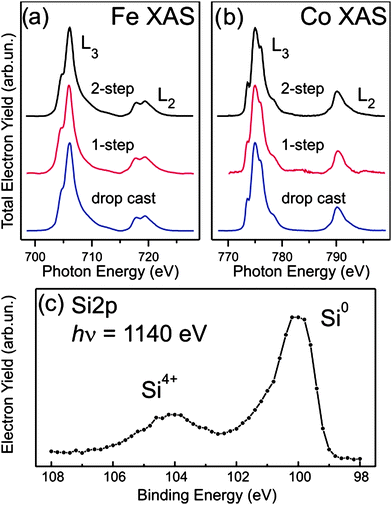 | ||
| Fig. 3 Characterization of embedded nanoparticles. (a) XAS spectra of Fe and (b) Co L2,3 absorption thresholds for embedded NPs compared with spin coated NPs thick film. (c) Si2p photoelectron spectra collected with photon energy 1140 eV over different positions of a sample surface with NPs embedded by 2-step process. | ||
XPS analysis has been employed to probe the chemical state of the other elements of the surface. The species detected at the surface by XPS were Si (Si2p), O (O1s), and C (C1s). The O1s and C1s signals are not very meaningful because of the overlap of several contributions from the embedded material, residuals of the solvent used for the deposition process and surface contaminants due to air exposure before insertion in the UHV chamber (e.g. CO2, H2O, hydrocarbons, etc.). Conversely, the Si2p signal is only related to the silicon substrate and distinguishes clearly between valence states associated to different chemical species. The Si2p XPS spectrum shown in Fig. 3c was recorded for a sample surface with the NPs embedded by a 2-step process. The spectrum exhibits two strong peaks which are related to oxidized silicon distributed over the surface (Si4+, B.E. 104 eV, indicating the presence of SiO2) and to the underlying bare silicon (Si0, B.E. 100 eV), respectively. XAS and XPS spatial mappings of the surfaces were performed for all the samples. The branching ratio of the two signal intensities is preserved over the whole surface, thus indicating that after the embedding process the silicon oxide distribution is homogeneous. Slight variations among the Si2p spectra are reasonably explained by the minor presence of silicon chemical states related to different oxide stoichiometry28 and to surface contamination due to exposition to the air, being the samples prepared ex situ and analysed without any surface treatment after the transfer in vacuum for XPS and XAS measurements. Therefore these results support the ability of the embedding process to act effectively over macroscopic large-areas.
The magnetic characterization of embedded NPs was performed using a SQUID magnetometer. In Fig. 4 is reported the temperature dependence from 5 to 300 K of the zero field cooled (ZFC) and field cooled (FC) magnetization curves of as prepared NPs, spin coated and embedded NPs respectively. The curves were obtained with a 10 mT magnetic field that in the case of spin coated and embedded NPs was applied perpendicularly to the silicon slab. All samples display the typical behavior of single domain magnetic NPs: at room temperature all particles are in the superparamagnetic regime, consistent with the very small size of the NPs, while below ca. 300 K, thermal irreversibility occurs. No alteration of the magnetic properties was observed in embedded NPs with respect to the spin coated ones, whose behavior indeed resembles those of powder samples of non-deposited NPs (Fig. 4a). Eventually, it is worth to point out that no differences in the magnetic properties were observed when applying the magnetic field in the plane or perpendicularly to the plane of the slab. These results support the ability of the embedding process to act effectively over macroscopic large-area regions without alterations of magnetic properties in the embedded NPs.
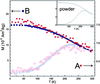 | ||
| Fig. 4 Temperature dependence of the zero field cooled (ZFC, open symbols) and field cooled (FC, full symbols) magnetizations of embedded NPs (A, red curves) compared to spin coated thin deposits (B, blue curves). The inset shows the magnetizations of as prepared (powder) NPs. | ||
Conclusions
In conclusion, we show that n-EM is a new additive approach able to integrate nano-objects into a surface in a controlled manner and with nanometric resolution. It offers a suitable method to organize nano-objects over a large scale embedded inside a thin oxide layer. The use of large stamps, the low cost for application and the possible integration with the current silicon technology pose n-EM as an ideal candidate for industrial implementation as a midterm application. Here we have demonstrated the feasibility of the method using CoFe2O4 NPs as a testing material and silicon as a substrate; however, the approach is general and can be extended to several other nano-objects and substrates. Although we expect an important impact of n-EM on basic science, a wealth of possible applications can be envisaged, in electronics as floating gates or for the fabrication of nanowires, in sensing as active materials, in catalysis and in high-density information storage.Acknowledgements
This work, as part of the ESF—European Young Investigators Awards Scheme, DYMOT, as well as from the EC Sixth and Seven Framework Programmes (NanoMagma, CP-FP-214107).Notes and references
- T. Vossmeyer, L. Katsikas, M. Giersig, I. G. Popovic, K. Diesner, A. Chemseddine, A. Eychmuller and H. Weller, J. Phys. Chem., 1994, 98, 7665–7673 CrossRef CAS.
- (a) A. Sanchez, S. Abbet, U. Heiz, W. D. Schneider, H. Hakkinen, R. N. Barnett and U. Landman, J. Phys. Chem. A, 1999, 103, 9573–9578 CrossRef CAS; (b) P. Greco, M. Cavallini, P. Stoliar, S. D. Quiroga, S. Dutta, S. Zacchini, M. C. Iapalucci, V. Morandi, S. Milita, P. G. Merli and F. Biscarini, J. Am. Chem. Soc., 2008, 130, 1177–1182 CrossRef CAS.
- (a) O. Ikkala and G. ten Brinke, Science, 2002, 295, 2407–2409 CrossRef CAS; (b) M. Melucci, G. Barbarella, M. Zambianchi, F. Biscarini, M. Cavallini, A. Bongini, M. Mazzeo and G. Gigli, Macromolecules, 2004, 37, 5692–5702 CrossRef CAS; (c) V. Corradini, C. Menozzi, M. Cavallini, F. Biscarini, M. G. Betti and C. Mariani, Surf. Sci., 2003, 532–535, 249–254 CrossRef CAS.
- A. P. Alivisatos, Science, 1996, 271, 933–937 CrossRef CAS.
- M. C. Daniel and D. Astruc, Chem. Rev., 2004, 104, 293–346 CrossRef CAS.
- (a) A. N. Shipway, E. Katz and I. Willner, ChemPhysChem, 2000, 1, 18 CrossRef CAS; (b) M. Surin, P. Sonar, A. C. Grimsdale, K. Müllen, S. De Feyter, S. Habuchi, S. Sarzi, M. Van der Auweraer, F. C. De Schryver, M. Cavallini, J.-F. Moulin, F. Biscarini, C. Femioni, R. Lazzaroni and P. Leclère, J. Mater. Chem., 2007, 17, 728–735 RSC.
- A. D. McFarland and R. P. Van Duyne, Nano Lett., 2003, 3, 1057 CrossRef CAS.
- M. Gratzel, J. Photochem. Photobiol., C, 2003, 4, 145–153 CrossRef CAS.
- (a) I. I. Naumov, L. Bellaiche and H. X. Fu, Nature, 2004, 432, 737–740 CrossRef CAS; (b) M. Cavallini, I. Bergenti, S. Milita, G. Ruani, I. Salitros, Z.-R. Qu, R. Chandrasekar and M. Ruben, Angew. Chem., Int. Ed., 2008, 47, 8596–8600 CrossRef CAS.
- D. Lee, M. F. Rubner and R. E. Cohen, Nano Lett., 2006, 6, 2305 CrossRef CAS.
- A. Tricoli, M. Graf, F. Mayer, S. Kuhne, A. Hierlemann and S. E. Pratsinis, Adv. Mater., 2008, 20, 3005–3010 CrossRef CAS.
- Z. Y. Tang, N. A. Kotov and M. Giersig, Science, 2002, 297, 237 CrossRef CAS.
- (a) M. Cavallini, J. Gomez-Segura, C. Albonetti, D. Ruiz-Molina, J. Veciana and F. Biscarini, J. Phys. Chem. B, 2006, 110, 11607 CrossRef CAS; (b) M. Cavallini, M. Facchini, C. Albonetti and F. Biscarini, Phys. Chem. Chem. Phys., 2008, 10, 784–793 RSC.
- (a) F. McKenzie, K. Faulds and D. Graham, Nanoscale, 2010, 2, 78 RSC; (b) H. Takagi, H. Ogawa, Y. Yamazaki, A. Ishizaki and T. Nakagiri, Appl. Phys. Lett., 1990, 56, 2379 CrossRef CAS.
- H. Mertens, J. Verhoeven and A. Pxolman, Appl. Phys. Lett., 2004, 85, 1317–1319 CrossRef CAS.
- S. Neralla, D. Kumar, S. Yarmolenko and J. Sankar, Composites, Part B, 2004, 35, 157–162 CrossRef.
- C. Graf, S. Dembski, A. Hofmann and E. Ruhl, Langmuir, 2006, 22, 5604–5610 CrossRef CAS.
- T. R. Sathe, A. Agrawal and S. M. Nie, Anal. Chem., 2006, 78, 5627 CrossRef CAS.
- (a) M. Cavallini, J. Gomez, D. Ruiz, M. Massi, C. Albonetti, C. Rovira, J. Veciana and F. Biscarini, Angew. Chem., Int. Ed., 2005, 44, 888–892 CrossRef CAS; (b) M. Cavallini, C. Albonetti and F. Biscarini, Adv. Mater., 2009, 21, 1043–1053 CrossRef CAS; (c) M. Cavallini, J. Mater. Chem., 2009, 19, 6085–6092 RSC; (d) M. Cavallini, M. Murgia and F. Biscarini, Nano Lett., 2001, 1, 193–195 CrossRef CAS.
- D. A. Serban, P. Greco, S. Melinte, S. Vlad, C. A. Dutu, S. Zacchini, M. C. Iapalucci, F. Biscarini and M. Cavallini, Small, 2009, 5, 1117 CAS.
- C. N. Chinnasamy, M. Senoue, B. Jeyadevan, O. Perales-Perez, K. Shinoda and K. Tohji, J. Colloid Interface Sci., 2003, 263, 80–83 CrossRef CAS.
- J. H. Tong, L. L. Bo, Z. Li, Z. Q. Lei and C. G. Xia, J. Mol. Catal. A: Chem., 2009, 307, 58–63 CrossRef CAS.
- P. Avouris, T. Hertel and R. Martel, Appl. Phys. Lett., 1997, 71, 285 CrossRef CAS.
- (a) R. Garcia, R. V. Martinez and J. Martinez, Chem. Soc. Rev., 2006, 35, 29–38 RSC; (b) F. C. Simeone, C. Albonetti and M. Cavallini, J. Phys. Chem. C, 2009, 113, 18987–18994 CrossRef CAS.
- (a) R. Maoz, E. Frydman, S. R. Cohen and J. Sagiv, Adv. Mater., 2000, 12, 725 CrossRef CAS; (b) M. Cavallini, P. Mei, F. Biscarini and R. García, Appl. Phys. Lett., 2003, 83, 5286–5288 CrossRef CAS; (c) C. Albonetti, J. Martinez, N. S. Losilla, P. Greco, M. Cavallini, F. Borgatti, M. Montecchi, L. Pasquali, R. Garcia and F. Biscarini, Nanotechnology, 2008, 19, 435303 CrossRef.
- F. De Groot and A. Kotani, Core Level Spectroscopy of Solids, Taylor & Francis Group, 6000 Broken Sound Parkway NW, Suite 300, 2008 Search PubMed.
- D. H. Kim, H. J. Lee, G. Kim, Y. S. Koo, J. H. Jung, H. J. Shin, J. Y. Kim and J. S. Kang, Phys. Rev. B: Condens. Matter Mater. Phys., 2009, 79, 033402 CrossRef.
- (a) F. J. Himpsel, F. R. McFeely, A. Taleb-Ibrahimi, J. A. Yarmoff and G. Hollinger, Phys. Rev. B: Condens. Matter, 1988, 38, 6084 CrossRef CAS; (b) D. Schmeisser, F. J. Himpsel and G. Hollinger, Phys. Rev. B: Condens. Matter, 1983, 27, 7813 CrossRef CAS.
Footnote |
| † Electronic supplementary information (ESI) available: Detailed method and characterization. See DOI: 10.1039/c0nr00315h |
| This journal is © The Royal Society of Chemistry 2010 |