Phototransport in networks of tetrapod-shaped colloidal semiconductor nanocrystals†
Isabella R.
Franchini
a,
Adriano
Cola
b,
Aurora
Rizzo
c,
Rosanna
Mastria
c,
Anna
Persano
b,
Roman
Krahne
a,
Alessandro
Genovese
a,
Andrea
Falqui
a,
Dmitry
Baranov‡
a,
Giuseppe
Gigli
c and
Liberato
Manna
*a
aIstituto Italiano di Tecnologia, Via Morego 30, 16163, Genova, Italy. E-mail: liberato.manna@iit.it
bIMM-CNR, Institute for Microelectronics and Microsystems – Unit of Lecce, Via Monteroni, I-73100, Lecce, Italy
cNational Nanotechnology Laboratory (NNL), CNR-Nanoscienze, Via per Arnesano km 5, I-73100, Lecce, Italy
First published on 3rd August 2010
Abstract
Tetrapod-shaped CdSe(core)/CdTe(arms) colloidal nanocrystals, capped with alkylphosphonic acids or pyridine, were reacted with various small molecules (acetic acid, hydrazine and chlorosilane) which induced their tip-to-tip assembly into soluble networks. These networks were subsequently processed into films by drop casting and their photoconductive properties were studied. We observed that films prepared from tetrapods coated with phosphonic acids were not photoconductive, but tip-to-tip networks of the same tetrapods exhibited appreciable photocurrents. On the other hand, films prepared from tetrapods coated with pyridine instead of phosphonic acids were already highly photoconductive even if the nanocrystals were not joined tip-to-tip. Based on the current–voltage behavior under light we infer that the tunneling between tetrapods is the dominant charge transport mechanism. In all the samples, chemically-induced assembly into networks tended to reduce the average tunneling barrier. Additionally, pyridine-coated tetrapods and the tip-to-tip networks made out of them were tested as active materials in hybrid photovoltaic devices. Overall, we introduce an approach to chemically-induced tip-to-tip assembly of tetrapods into solution processable networks and demonstrate the enhancement of electronic coupling of tetrapods by various ligand exchange procedures.
Introduction
There is a growing consensus that realizing the promises of nanoscience, such as new cost-effective optoelectronic devices, new materials for energy generation, or new nanocomposites for medical implants, will rely heavily on a bottom-up approach via assembly of nanoscale building blocks. Among the possible candidates, colloidal nanocrystals constitute a family of nanostructures most suitable for such a challenge. Research on the assembly of colloidal nanocrystals has been focused so far mainly on their organization in ordered superstructures, for example the creation of superlattices of monodisperse spherical nanocrystals, a field which is well advanced today.1Assembly of shape controlled nanocrystals like nanorods2 (and the study of their photoconductive properties),3 or of branched nanocrystals4 has also been investigated, although to a lower extent. Tip-to-tip assembly of these types of nanocrystals, to form one dimensional arrays (for nanorods), or 3D network structures (for branched nanocrystals) is hard to tackle but nonetheless is a technologically important research field. For example, it could lead to the fabrication of nanocomposite fibers with controllable and combined mechanical, electric, thermoelectric, or photo-conductive behavior, to cite a few, or to lightweight, high performing materials useful in catalysis or in tissue engineering. Some reports of tip-to-tip assembly of shape-controlled nanocrystals, mainly nanorods, have appeared so far, which exploited the higher reactivity of nanorod tips towards the binding of organic molecules or the growth of domains of other materials that could mediate tip-to-tip nanocrystal organization.5
Tetrapod-shaped colloidal nanocrystals of semiconductors are a popular class of branched nanocrystals and have been exploited in various applications, most notably in thin-film photovoltaic devices based mainly on blends with organic molecules and/or polymers.6,7 The efficiency of these types of devices is governed by many parameters, one of which is electron transport in the active layer, which proceeds via electrons moving from nanocrystal to nanocrystal. Efficient electron transport requires the presence of “percolating” pathways for electrons, hence arrays made of nanocrystals that are sufficiently close to each other and which connect the anode and the cathode of the device. Attempts to improve transport through films of nanocrystals have involved high-temperature annealing in order to fabricate network structures of interlinked nanocrystals, such that direct electrical contact of a large number of nanocrystals was guaranteed, hence more pathways for electrons throughout the whole layer were created.8
We propose here an alternative approach for the fabrication of network structures of tetrapods, based on the pre-organization of semiconductor CdSe(core)/CdTe(arms) tetrapods into stable and soluble aggregates already in the solution phase, which can be potentially useful in photovoltaic applications, e.g. as inks for printable solar cells. To this aim we exploited the higher reactivity of the tips of the tetrapod arms, compared to other regions of the tetrapod surface, under various chemical treatments. The preferential removal of surfactants from these regions, or their exchange with short molecules, led to destabilization of the tips, which caused aggregation of the tetrapods in solution, such that they started organizing in tip-to-tip connected three-dimensional network structures that were still soluble. Solutions of these networks were drop-cast on substrates, yielding nanocrystal films upon solvent evaporation.
We found that nanocrystal films prepared from as-synthesized tetrapods, coated at their surface with alkylphosphonic acids (hence as they were obtained from the synthesis), exhibited no photocurrent, while their organization into networks in solution (upon reaction with various molecules) yielded films with appreciable photocurrent (few pA at 0.5 V μm−1). For comparison, films prepared from non-assembled tetrapods, but capped with pyridine instead of phosphonic acids, exhibited already much higher photoconductivity (few nA at 0.5 V μm−1). Notably, there was no substantial variation in phototransport if pyridine-capped tetrapods were assembled into networks.
In order to investigate the possibility to integrate the network structures as photoactive materials in hybrid solar cells, the tetrapods coated with pyridine were chosen because of their higher photoconductivity. Compared to the devices prepared with non-assembled tetrapods, those prepared with networks assembled via chlorosilane and hydrazine showed a slight reduction in their performances (as discussed herein), while those prepared with networks assembled via acetic acid showed a slight improvement. Note that hereinafter throughout the text terms “assembled” and “assembly” refer to tip-to-tip joined tetrapods forming a network.
Experimental
The nanocrystal samples in our experiments were tetrapods with four wurtzite CdTe arms and a central sphalerite CdSe region, which were synthesized by a seeded growth approach that was recently developed in our group.9 These samples had uniform arm lengths and were contaminated by a negligible fraction of shapes other than tetrapods (see Fig. 1a). In one series of experiments the starting nanocrystals were the as-synthesized particles capped with phosphonic acids (hexylphosphonic and octadecylphosphonic acid), cleaned from most of the excess of surfactants, by repeated washing with methanol and re-dissolution in toluene. In another series of experiments, the starting nanocrystals first underwent a surfactant exchange procedure with pyridine (i.e. the original phosphonic acids were replaced with pyridine, see the ESI†). These nanocrystals were then dissolved in a pyridine/chloroform mixture (1![[thin space (1/6-em)]](https://www.rsc.org/images/entities/char_2009.gif) :9 volume ratio of the solvents). Pyridine molecules are short and weakly coordinating ligands for nanocrystals, and are widely used for coating nanocrystals to be used in photovoltaic cells, because they increase coupling among nanocrystals and between nanocrystals and polymers.10
:9 volume ratio of the solvents). Pyridine molecules are short and weakly coordinating ligands for nanocrystals, and are widely used for coating nanocrystals to be used in photovoltaic cells, because they increase coupling among nanocrystals and between nanocrystals and polymers.10
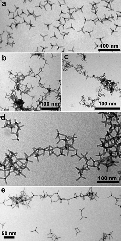 | ||
| Fig. 1 (a) Wide-field low magnification TEM image of CdSe@CdTe tetrapods prepared by the seeded-growth approach and coated with alkylphosphonic acids. The tetrapods consist of CdSe ‘sphalerite’ seeds, onto which four wurtzite CdTe arms were grown; (b–c) the same tetrapods assembled by addition of acetic acid, followed by sonication for 30 min; (d) by addition of trimethylchlorosilane; and (e) by addition of hydrazine. The solvent in all cases was toluene. The samples were freshly prepared in solution, a drop of solution was deposited on a carbon coated copper grid, and the solvent was allowed to evaporate. The networks imaged under TEM represent what is left under solvent evaporation. It is possible that they differ from the networks in solution by many aspects, because several processes might occur during evaporation: bigger networks might break into smaller networks as a result of convective flow; separate smaller networks might aggregate at the later stages of solvent evaporation due to strong van der Waals interactions; a network could partly collapse as a result of escape of solvent that was previously entrapped in between the tetrapods. | ||
For both types of ligand-coated tetrapods we followed three different procedures in order to destabilize the tip regions of the tetrapods. These were: (i) addition of acetic acid, followed by sonication for 30 min at room temperature. A similar procedure, although involving an amine, was found by O'Sullivan et al. to induce oriented attachment in CdS and Ag2S nanorods;11 (ii) addition of trimethylchlorosilane, which is known to strip off alkylphosphonates from the surface of nanocrystals efficiently;12 (iii) addition of hydrazine, a strongly coordinating bi-dentate ligand which displaces surfactants from the surface of the nanocrystals and promotes nanocrystal-to-nanocrystal bridging, and like pyridine can be removed by mild thermal treatment.13 The influence of hydrazine on the electronic and transport properties of nanocrystal films has been studied in recent years.13,14
All the procedures above were refined in order to identify the amount of reagents that had to be added such that the networks of tetrapods formed were still stable in solution (see the ESI†). Optical absorption spectra were recorded from solutions containing the various samples. For transmission electron microscopy (TEM) analysis, a drop of solution was deposited on a carbon coated copper grid, and the solvent was allowed to evaporate. Additionally, TEM analysis was carried out on representative grids after they had been annealed at 450 K for 30 min under vacuum, to check if any structural transformation occurred upon annealing.
Ti/Au (3/30 nm) interdigitated electrodes, 2 μm spaced, covering a total active area of about 25 × 25 μm2, were deposited by standard photolithography and lift-off on Si/SiO2 substrates. Solutions of the various nanocrystal samples were deposited by drop casting onto these interdigitated electrodes. Then samples were annealed at 450 K for 30 min under low vacuum (p ∼ 10−3 torr).
Current–voltage scans, both under white light illumination and in the dark, were carried on all the films in air at room temperature in an electromagnetically shielded K. Suss PM5 probe station, using a HP 4140B pA meter/DC voltage source, in order to apply the bias voltage at one electrode and measure the current at the other electrode. In photocurrent spectral experiments, a 100 W tungsten halogen lamp in combination with a 0.11 m monochromator was used as the excitation source. Light intensity was monitored with a calibrated Si photodiode in order to evaluate the total incident optical power and to normalize the device photocurrent spectra. After all transport measurements were carried out, the samples were inspected by scanning electron microscopy (SEM).
Photovoltaic (PV) devices were fabricated in a bilayer configuration. Concentrated solutions (≈ 60 mg ml−1) of different pyridine-coated tetrapods (non-assembled, assembled via acetic acid, via hydrazine and via chlorosilane) were prepared (see the ESI for details†) and deposited by spin-coating at 1500 rpm onto indium tin oxide (ITO) substrates coated with PEDOT:PSS.15 The samples were annealed on a hot plate at 150 °C for 20 min and held at 6 × 10⁻⁶ mbar overnight, after which a 30 nm thick layer of C60 was deposited by thermal evaporation and a 130 nm thick aluminium cathode was evaporated on it through a shadow mask. Finally the samples underwent a second annealing step at 150 °C for 30 min. All manipulations, except for the PEDOT:PSS deposition, were performed in a glove box under nitrogen atmosphere. Before their characterization, all devices were sealed using a glass lid attached by a bead of UV-cured epoxy resin. Current–voltage characteristics of the PV devices were studied using a Keithley 2400 Source Measure Unit and a solar simulator Spectra Physics Oriel 150 W with AM 1.5G filter set. The integrated intensity was set to 100 mW cm−2 using a thermopile radiant power meter with fused-silica window (Spectra Physics Oriel, model 70260).
Results and discussion
Structural and morphological characteristics of the networks
In nanocrystals coated with phosphonic acids (Fig. 1), each of the three assembling procedures led to the formation of assembled structures, with tetrapods bound to each other mainly via their tips, as could be seen from transmission electron microscopy (TEM) images of nanocrystals deposited on a TEM grid after solvent evaporation (Fig. 1b–e). The degree of assembly varied depending on the amount of molecules (either acetic acid, hydrazine or chlorosilane) added to nanocrystals, and time of reaction. Beyond a certain threshold in this ratio (typically an excess of additives), or in time lapse after addition of the molecules, the solutions became turbid and a precipitate started forming at the bottom of the vial (see the ESI†).In the case of pyridine-coated nanocrystals, large aggregates of tetrapods were observed already on grids prepared by deposition of the solution containing non-assembled nanocrystals, hence before any assembly treatment (Fig. 2a). In these aggregates, tetrapods appeared however to prefer side-to-side interactions, most likely due to the strong van der Waals interactions between these nanocrystals due to the short pyridine ligands coating their surface. As the starting non-assembled samples in pyridine were stable in solution, it is likely that the aggregates seen under TEM were not formed in solution, but rather during the last stages of solvent evaporation on the grid. Samples of pyridine-coated nanocrystals assembled into networks showed both side-to-side and tip-to-tip assembly (Fig. 2b-e).
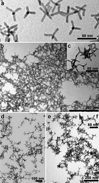 | ||
| Fig. 2 (a) Wide-field low magnification TEM image of the same CdSe@CdTe tetrapods as shown in Fig. 1a, after their phosphonic acid surfactants were exchanged with pyridine; TEM images of these pyridine coated tetrapods organized into networks upon reaction with: (b–c) acetic acid, followed by sonication for 30 min; (d) trimethylchlorosilane; (e–f) hydrazine. In (f) several junctions can be seen between tetrapods. | ||
High-resolution TEM (HRTEM) analysis on the various networks indicated that in general there were no preferential epitaxial relationships between touching arms (Fig. 3). Occasionally, two arms belonging to different tetrapods shared a very small (1–2 nm wide) sphalerite domain, but most often the interfacial region between two touching arms was amorphous. Oriented attachment in these nanocrystals is hard to achieve, because all the tips of tetrapod arms have the same polarity, as they have wurtzite structure. This is different from the case of wurtzite nanorods, which indeed expose both opposite tip regions along their elongation direction to the external environment. Hence oriented attachment in a head-to-tail arrangement of the respective lattice polarities is possible for wurtzite nanorods and has been observed.11 By contrast, no attachment between arms belonging to two tetrapods could result in a straight junction made of a single crystalline domain (see Fig. 3 for example). On the other hand a small sphalerite domain can bridge the two arms by linking each arm via one of its (111) facets, and the arms bind to this domain via their (001) facets (see Fig. 3d). Sphalerite domains could be located occasionally on the tip of an arm as a consequence of the defective growth of the arms during the tetrapod synthesis, so that wurtzite regions are interrupted by a few layers of sphalerite structure, especially in tetrapods with CdTe arms.9 In other cases, the linking between the arms occurred either by means of amorphous regions (Fig. 3e), or by bridging molecules which brought tips close to each other, but without direct touching. Even though all solutions contained the same concentration of tetrapods, when they were deposited on substrates with interdigitated electrodes the resulting film thickness varied from roughly one monolayer of tetrapods to approximately three monolayers (as seen by SEM). A representative SEM image of tetrapod film in between electrode structures is shown in Fig. 4.
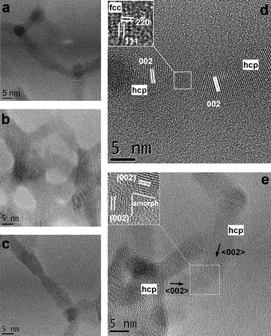 | ||
| Fig. 3 (a–c) Low-magnification HRTEM images of the CdSe@CdTe tetrapods networks showing several zones where attachment between tetrapod arms had occurred. (d) High magnification HRTEM of tips of wurtzite CdTe arms belonging to two different tetrapods and connected by a small sphalerite CdTe crystalline domain or (e) by an amorphous region. | ||
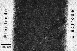 | ||
| Fig. 4 Scanning electron microscopy (SEM) image of a typical device showing pyridine coated tetrapods, linked via reaction with hydrazine into network structures, in the region between two electrodes. More SEM images are reported in the ESI.† | ||
Transport properties of films of “non-assembled” tetrapods
Current–voltage (I–V) characteristics of the “as-deposited” (i.e. without any annealing) nanocrystal films (both phosphonic-acid and pyridine coated) evidenced measurable dark currents, much higher for the pyridine-coated samples (see the ESI†), but affected in all cases by significant current transients and hysteresis during the voltage cycles. These effects could be explained by the presence of residual solvent molecules and/or excess unbound surfactants (or yet other organic molecules) in the film, which can provide intermediate states contributing to the carrier transport between tetrapods (see the ESI†), and which could be removed by annealing. Additionally, no photocurrent was observed from the phosphonic-acid coated samples.After annealing, in the sample of pyridine-coated tetrapods, the I–V characteristics became stable and reproducible with negligible hysteresis, but both dark current and photocurrent of the films decreased (Fig. 5a). The decrease in photocurrent might be correlated with the increased tendency of the samples towards oxidation, once a film of organic contaminants had been removed. The same annealing treatment on the sample coated with phosphonic acids caused the dark current to fall below the instrument detection limit, while still no photocurrent could be detected (Fig. 5e). As a control experiment, inspection of TEM grids on which tetrapod networks had been deposited, evidenced that no structural changes on the networks had occurred due to annealing (see the ESI†).
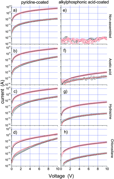 | ||
| Fig. 5 I–V curves in the dark (black open squares) and under white light (red circles) for pyridine-coated and annealed and samples that were not assembled (a) and assembled with acetic acid (b), hydrazine (c), and chlorosilane (d). Panels (e–h) refer to phosphonic acid-coated and annealed samples, respectively non-assembled (e) and after the same assembly treatments as for pyridine-coated samples (f–h). Solid lines are least-squared fits to I–V curves in the dark and under white light with eqn (1). | ||
Despite the complexity of the carrier transport mechanisms, involving exciton ionization, transport across tetrapods, injection from contacts, the I–V behaviour of the films could be qualitatively explained in terms of tunneling. This is in agreement with the work of Porter et al. for films of CdTe nanocrystals, where similar transport studies using gold electrodes in planar configuration were carried out.16 Following Drndić and Porter's approach,16,17 we assume an exponential dependence of the current on the voltage that can be modeled as:
 | (1) |
Here V is the applied voltage, R0light is the equivalent zero-field resistance which depends on the number of conducting channels and in thus also scales inversely with the film thickness, and V0 is a characteristic voltage that gives a measure for the tunnel barriers which have to be overcome in a conductive path connecting the electrodes. V0 therefore scales linearly with the electrode distance, and by dividing V0 by the average number of nanocrystals that form a conductive path (in our case around 50 tetrapods are needed to connect the 2 μm spaced electrodes) one can obtain an averaged value for the potential barrier in between individual nanoparticles.16 Using this fitting model we obtain V0 = 51.4 V and R0light = 1.9 GΩ (Table 1, second row) for films of pyridine-coated tetrapods. These values are comparable to those obtained by Drndić et al. and Porter et al.16,17 for densely packed spherical CdTe and CdSe nanocrystal films. Dividing V0 by 50, i.e. the number of tetrapods that are needed to bridge the electrode gap of 2 μm, yields 1 V for the average potential barrier between two adjacent nanocrystals. However, we note that for films consisting of tetrapods, due to the intrinsic complexity of the tetrapods assembly in three dimensions, involving a multitude of mutual spatial configurations for neighboring nanocrystals, it is not straightforward to correlate V0 quantitavely to a specific and unique potential barrier between two adjacent nanocrystals. Furthermore, the fact that no photocurrent was measured on the tetrapod samples coated with phosphonic acids suggests that these large molecules represent insuperably high potential barriers for the charge carriers.
| V 0/V | R 0light/GΩ | R 0dark/R0light | |
|---|---|---|---|
| Pyridine-coated “non-assembled” | 51.4 | 1.9 | 60.3 |
| Pyridine-coated “networks” (hydrazine) | 13.9 | 2.0 | 43.8 |
| Pyridine-coated “networks” (acetic acid) | 17.9 | 2.2 | 72.5 |
| Pyridine-coated “networks” (chlorosilane) | 7.2 | 25.4 | 42.8 |
| Phosphonic acids-coated “non-assembled” | N A | NA | NA |
| Phosphonic acids-coated “networks” (hydrazine) | 27.5 | 226 | 58.3 |
| Phosphonic acids-coated “networks” (acetic acid) | 11.3 | 2.2 × 10⁴ | 2.9 |
| Phosphonic acids-coated “networks” (chlorosilane) | 15.5 | 253 | 85.9 |
Porter additionally points out that the dark I–Vs can be explained by the same functional expression as of eqn (1), albeith with a different set of parameters.16 Indeed, the I–V curve under dark is also reasonably fitted by eqn (1) (Fig. 5). In this new fit the R0light parameter is replaced with R0dark. The R0dark/R0light can be considered as a valuable figure of merit for the photoresponse, since a material with a high R0dark/R0light ratio is suitable for photovoltaics. The R0dark/R0light ratios calculated for the various samples studied here are reported in Table 1 (last column).
Transport properties of films of “networked” tetrapods
We address now the photoconduction properties of networks of tetrapods, prepared according to the three different treatments discussed in the Experimental section. We will consider hereafter only the annealed samples, as they exhibited stable, non-hysteretic behaviour (experimental data are reported in Fig. 5 and the fit parameters in Table 1). Overall, the networking procedure caused a lowering of V0, which means that the inter-tetrapod barrier was lowered. For example, with respect to the “non-assembled” sample, the assembly with hydrazine yielded films characterized by a substantial reduction of V0 from 51 to 14 V. Films from networks assembled via acetic acid gave similar results in terms of V0, while films from networks assembled via chlorosilane exhibited the smallest V0, but also the highest R0light values of all films prepared from networks, despite their film thickness did not appear to be much different from that of the other samples. For what concerns the R0dark/R0light ratio, among the samples coated with pyridine the one treated with acetic acid was characterized by the highest value. We note that an increase in the R0dark/R0light ratio (see Table 1) was not always accompanied by a decrease in V0.All the treatments of phosphonic-acid coated tetrapods to form networks gave rise to a notable photocurrent signal. The signal was much lower than that of the corresponding pyridine samples. One minor reason for this could be the variation in film thickness, but we remind that films from non-assembled tetrapods in this case were not conductive. Hence, considering that transport though phosphonic acid coated samples is much more difficult than for pyridine-coated nanocrystals, the assembly here has the effect of opening at least one transport channel in between tetrapods, namely tunneling from tip to tip. The dark currents in these sets of samples became measurable too, although they were remarkably low (below 10−13 A at 0.5 V μm−1).
The V0 values of the phosphonic acid-coated samples were in the same range as those of the films made from pyridine coated tetrapods, but the R0light were much higher, which is expected since transport in these networks should occur only from tip to tip, hence the films overall are more resistive. One has to keep in mind however that the comparisons among the various R0light and among the R0dark/R0light ratios are to be taken with care, since they also depend on film thickness.
Photocurrents and optical absorption spectra
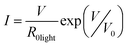
We discuss here only the photocurrent spectra of the various films of pyridine-coated tetrapod samples, both the non-assembled tetrapods and the corresponding networks prepared with the various approaches, after annealing. These are reported in Fig. 6 and compared with the optical spectra of the corresponding pyridine/chloroform solutions from which the films had been prepared (solutions for optical spectra were actually more diluted than those used to prepare films). All photocurrent spectra were blue-shifted with respect to the optical spectra, indicating possible shrinkage in size of the tetrapods in the film. The photocurrents followed a trend similar to that of the absorption spectra, namely an onset at longer wavelengths, with the signal then increasing at shorter wavelengths. This proved that the current measured under white light irradiation originated indeed from carrier generation and extraction from the tetrapods in the films. This was particularly evident for the film made of non-assembled tetrapods and for that of networks prepared with acetic acid. In all the spectra, the dominant feature is the absorption/photocurrent from carriers originated in the CdTe arms, and there is no evidence of signal due spatially indirect transitions associated with the type-II band alignment between the CdSe core and the CdTe arms. This should be seen as a long tail extending to the infrared region. One must keep in mind however that the contribution of the CdSe core in these samples is almost negligible in terms of absorbance, therefore any absorption band due to spatially indirect transition is extremely weak. Type-II carrier recombination instead, with associated emission in the infrared region, has been observed by us in solutions of isolated CdSe/CdTe tetrapods and was reported in a previous work.9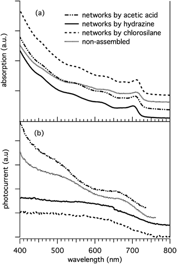 | ||
| Fig. 6 (a) Optical absorption spectra of tetrapods coated with pyridine. Exchange of surfactant with pyridine led to a blue shift of about 3–4 nm of the lowest exciton absorption peak (which is basically due to absorption from the CdTe arms in these samples), with respect to the as-synthesized tetrapods coated with phosphonic acids. This indicates a moderate etching of the surface of the nanocrystals, hence contraction in diameter. The various treatments aiming at network formation had instead little effect on the optical spectra of the nanocrystals, with respect to the pyridine-coated, non-assembled sample, except for hydrazine, which caused a substantial blue shift (around 10 nm). This can be explained by the stronger etching behavior of this type of molecule. (b) Photocurrent spectra from annealed films made from the same samples. | ||
Both films prepared from networks made with hydrazine and with chlorosilane exhibited photocurrents lower than expected in the region below 500 nm. While the origin of this behavior is not entirely clear at present, it is worth pointing out that both hydrazine and chlorosilane treatments are considerably more aggressive for the tetrapods than the acetic acid treatment. Exposure of tetrapods at increasing concentrations of hydrazine or chlorosilane, apart from inducing aggregation of the nanocrystals, were found to lead to severe etching of their surface, along with the collateral nucleation of very small nanocrystals (1–3 nm diameter), most likely arising from re-crystallization of atomic species stripped from the surface of the tetrapods. Eventually, exposure to large concentrations of these aggressive chemicals was found to completely reshape the tetrapods. Much less pronounced effects were seen on the other hand for exposure to increasing concentrations of acetic acid molecules. Hence low photocurrents at high irradiation energies for hydrazine and chlorosilane-treated samples might be related to the presence of small nanocrystals and/or organometallic clusters which might absorb light in this range but might not contribute to transport.
Photovoltaic devices based on tetrapods and network structures
The photovoltaic device structure fabricated using the various pyridine-coated tetrapod samples (non-assembled tetrapods, networks of tetrapods assembled via acetic acid, via hydrazine or via chlorosilane) is schematically represented in Fig. 7a. The device architecture follows closely a previous work by us on photovoltaic devices based on tetrapods.7 In the device, the CdSe@CdTe tetrapods act as electron donors, and the C60 works as electron acceptor and transport layer. After light absorption and exciton formation, the charge separation occurs either at the interface between the two materials or in the tetrapods heterostructure, i.e. the electrons are trapped in the CdSe core and the holes in the CdTe arms. The electrons in the C60 diffuse through the aluminium cathode and the holes in the tetrapods diffuse into the ITO anode.7 The current–voltage characteristics of the various photovoltaic devices are reported in Fig. 7b. The corresponding device performances are listed in Table 2.| PCE (%) | FF | V oc/V | J sc/mA cm−2 | |
|---|---|---|---|---|
| Non-assembled | 0.14 | 0.32 | 0.38 | 1.15 |
| Networks acetic acid | 0.21 | 0.46 | 0.38 | 1.19 |
| Networks hydrazine | 0.07 | 0.43 | 0.40 | 0.38 |
| Networks chlorosilane | 0.10 | 0.41 | 0.42 | 0.60 |
 | ||
| Fig. 7 (a) Schematic of the photovoltaic device structure. The active layer consists of a bilayer of either tetrapods or networks, and fullerene (C60). (b) Current–voltage characteristics for photovoltaic cells made with non-assembled pyridine-coated tetrapods, and with networks prepared with acetic acid, hydrazine and chlorosilane, respectively, under illumination of one-sun (AM 1.5 G). | ||
The device made with networks assembled via acetic acid had a power conversion efficiency (PCE) that was slightly higher than that of the device made with non-assembled tetrapods. The short circuit current (Jsc), which represents the maximum photogenerated current, is similar for these two devices. Also, both devices have the same open circuit voltage. As a consequence, the lower PCE for the device made with non-assembled tetrapods is due to the reduced field factor (FF). The lower FF is related to a higher series resistance of the cell, which arises from the resistance of the materials to current flow.18 On the other hand, the lower PCE for the devices made with networks prepared via hydrazine and chlorosilane results from a lower Jsc rather than a lower FF. This preliminary comparative study on the device performances suggests that the use of networks of tetrapods might help to improve the hole conductivity, i.e. a reduction of the resistance to the holes current flow, which results in higher FF values.
With respect to the device made with non-assembled nanocrystals, the photocurrent was improved slightly only for the device made with networks of tetrapods assembled with acetic acid, while it was actually reduced for devices made with networks assembled with hydrazine or with chlorosilane. The two latter treatments appear to have a negative impact on the charge separation mechanism at the interface with the C60 layer. The better performance of the devices based on non-assembled tetrapods and on the networks prepared with acetic acid was also confirmed in terms of the R0dark/R0light values of the corresponding films (Table 1). These findings could be explained by considering two possible implications connected with our procedures: (1) different effects of the chemical treatment on the tetrapods in the case of acetic acid with respect to chlorosilane and hydrazine; (2) morphology differences (grain size) in the resulting films, which influence charge separation between the tetrapods and C60. Based on previous reports,19 a hydrazine treatment of CdTe films for photovoltaic applications can lead to detrimental results. It can promote for example the formation of a thin insulating layer of CdTeO3, which can affect negatively device efficiency. The chlorosilane treatment, as was originally reported,15 inevitably leaves chlorine atoms on the surface of nanocrystals. In analogy with studies on bulk CdTe,20 chlorine doping (either by Cl2(g) treatment or by CdCl2 deposition) may result in reduced device performance. Preliminary atomic force microscopy (AFM) studies on the morphology of tetrapod films prepared by us have revealed that the average grain size in films of acetic acid treated tetrapods is smaller than in case of hydrazine or chlorosilane treatments (see the ESI for additional details†). In this scenario, acetic acid behaves rather as a short ligand, which replaces in part the molecules bound to the surface of nanocrystals (with preference at the tips), without affecting drastically the local chemical environment of tetrapods.
Conclusions
In this work we have reported various procedures for assembling tetrapod-shaped CdSe@CdTe colloidal nanocrystals into soluble networks of tip-to-tip aggregated nanocrystals. This attachment lowered the barrier for charge tunneling between neighboring tetrapods, especially for nanocrystals coated with bulk and insulating alkylphosphonic ligands it led to films with an appreciable photocurrent, while the films of non-assembled tetrapods were not photoconductive at all. The various chemical treatments that yielded tetrapod networks were tested in the preparation of photovoltaic devices. Considering the results of current–voltage characteristics, photocurrent spectra, and device efficiencies, it appears that less aggressive chemical treatments, like the one employing acetic acid, are effectively improving charge transport across multiple tetrapods and hence in creating pathways for carriers, without apparent disruption of the chemical structure of the nanocrystals and of the other components of the device. More aggressive treatments, like the ones involving hydrazine or chlorosilane, appear instead to be detrimental for the performance of photovoltaic devices. A special comment must be made on hydrazine treatment, which has been reported to improve the transport properties in close packed arrays of spheres and aligned nanorods.1,3 The main reason for such improvement is that surfactant replacement with hydrazine reduces inter-particle distance and thereby shortens the width of the tunnel barriers that the charges have to overcome. In the case of tetrapods, their branched shape does not allow a dense packing in which the inter-particle distance is dominated by the length of the surface ligands. Therefore, networks of tetrapods do not show such a dramatic increase in conductivity as observed in arrays of spherical particles and aligned rod arrays. Additionally, as we have discussed before, hydrazine treatment of CdTe can negatively affect the device efficiency. To the best of our knowledge, there have been no reports so far about hydrazine treatment performed on assemblies of colloidal CdTe nanoparticles and on how such treatment could affect their electronic properties.The advantage of tetrapod networks, for example for hybrid organic–inorganic photovoltaic devices, is on one hand their porous structure that provides large interfacial areas with organic molecules/polymers in order to collect one type of photo-excited charge carriers, while on the other hand the barriers for the collection of the second carrier type are reduced in the all-inorganic networks formed by the tip–tip assembly of the tetrapods, as is demonstrated by the results of our fitting model. Another advantage might be that tetrapods are 3D structures, therefore exploiting tip-to-tip assembly could lead to the highly porous 3D conductive networks or aerogels accessible through solution-based chemistry, while neither dots nor rods would provide this opportunity.
Acknowledgements
Financial support via the FP7 starting ERC grant NANO-ARCH (contract number 240111) is acknowledged. The authors gratefully acknowledge Sonia Carallo for technical support in the AFM imaging.Notes and references
- D. V. Talapin, J. S. Lee, M. V. Kovalenko and E. V. Shevchenko, Chem. Rev., 2010, 110, 389 CrossRef CAS.
- K. M. Ryan, A. Mastroianni, K. A. Stancil, H. T. Liu and A. P. Alivisatos, Nano Lett., 2006, 6, 1479 CrossRef CAS; B. Sun and H. Sirringhaus, J. Am. Chem. Soc., 2006, 128, 16231 CrossRef CAS; S. Gupta, Q. L. Zhang, T. Emrick and T. P. Russell, Nano Lett., 2006, 6, 2066 CrossRef CAS; S. Ahmed and K. M. Ryan, Nano Lett., 2007, 7, 2480 CrossRef CAS; T. Wetz, K. Soulantica, A. Falqui, M. Respaud, E. Snoeck and B. Chaudret, Angew. Chem., Int. Ed., 2007, 46, 7079 CrossRef CAS; C. Querner, M. D. Fischbein, P. A. Heiney and M. Drndic, Adv. Mater., 2008, 20, 2308 CrossRef CAS; J. Q. Zhuang, A. D. Shaller, J. Lynch, H. M. Wu, O. Chen, A. D. Q. Li and Y. C. Cao, J. Am. Chem. Soc., 2009, 131, 6084 CrossRef CAS; A. Sanyal, T. Bala, S. Ahmed, Ajay Singh, A. V. Piterina, T. M. McGloughlin, F. R. Laffir and K. M. Ryan, J. Mater. Chem., 2009, 42, 6421 Search PubMed; A. Guerrero-Martinez, J. Perez-Juste, E. Carbo-Argibay, G. Tardajos and L. M. Liz-Marzan, Angew. Chem., Int. Ed., 2009, 48, 9484 CrossRef CAS; N. Zhao, K. Liu, J. Greener, Z. H. Nie and E. Kumacheva, Nano Lett., 2009, 9, 3077 CrossRef CAS; J. L. Baker, A. Widmer-Cooper, M. F. Toney, P. L. Geissler and A. P. Alivisatos, Nano Lett., 2010, 10, 195 CrossRef CAS; D. Baranov, A. Fiore, M. Van Huis, C. Giannini, A. Falqui, U. Lafont, H. Zandbergen, M. Zanella, R. Cingolani and L. Manna, Nano Lett., 2010, 10, 743 CrossRef CAS; X. L. Fang, Y. Li, C. Chen, Q. Kuang, X. Z. Gao, Z. X. Xie, S. Y. Xie, R. B. Huang and L. S. Zheng, Langmuir, 2010, 26, 2745 CrossRef CAS.
- D. Steiner, D. Azulay, A. Aharoni, A. Salant, U. Banin and O. Millo, Phys. Rev. B: Condens. Matter Mater. Phys., 2009, 80, 195308 CrossRef; A. Persano, M. De Giorgi, A. Fiore, R. Cingolani, L. Manna, A. Cola and R. Krahne, ACS Nano, 2010, 4, 1646 CrossRef CAS.
- Y. Cui, M. T. Bjork, J. A. Liddle, C. Sonnichsen, B. Boussert and A. P. Alivisatos, Nano Lett., 2004, 4, 1093 CrossRef CAS; H. T. Liu and A. P. Alivisatos, Nano Lett., 2004, 4, 2397 CrossRef CAS.
- K. K. Caswell, J. N. Wilson, U. H. F. Bunz and C. J. Murphy, J. Am. Chem. Soc., 2003, 125, 13914 CrossRef CAS; B. F. Pan, L. M. Ao, F. Gao, H. Y. Tian, R. He and D. X. Cui, Nanotechnology, 2005, 16, 1776 CrossRef CAS; A. Salant, E. Amitay-Sadovsky and U. Banin, J. Am. Chem. Soc., 2006, 128, 10006 CrossRef CAS; G. Kawamura, Y. Yang and M. Nogami, J. Phys. Chem. C, 2008, 112, 10632 CrossRef CAS; A. Figuerola, I. R. Franchini, A. Fiore, R. Mastria, A. Falqui, G. Bertoni, S. Bals, G. Van Tendeloo, S. Kudera, R. Cingolani and L. Manna, Adv. Mater., 2009, 21, 550 CrossRef CAS.
- B. Q. Sun, H. J. Snaith, A. S. Dhoot, S. Westenhoff and N. C. Greenham, J. Appl. Phys., 2005, 97; D. J. Milliron, I. Gur and A. P. Alivisatos, Mrs Bullet., 2005, 30, 41 Search PubMed; Y. Zhou, Y. C. Li, H. Z. Zhong, J. H. Hou, Y. Q. Ding, C. H. Yang and Y. F. Li, Nanotechnology, 2006, 17, 4041 CrossRef CAS; Y. Q. Li, R. Mastria, K. C. Li, A. Fiore, Y. Wang, R. Cingolani, L. Manna and G. Gigli, Appl. Phys. Lett., 2009, 95.
- Y. Q. Li, R. Mastria, A. Fiore, C. Nobile, L. X. Yin, M. Biasiucci, G. Cheng, A. M. Cucolo, R. Cingolani, L. Manna and G. Gigli, Adv. Mater., 2009, 21, 4461 CrossRef CAS.
- I. Gur, N. A. Fromer, M. L. Geier and A. P. Alivisatos, Science, 2005, 310, 462 CrossRef CAS.
- A. Fiore, R. Mastria, M. G. Lupo, G. Lanzani, C. Giannini, E. Carlino, G. Morello, M. De Giorgi, Y. Li, R. Cingolani and L. Manna, J. Am. Chem. Soc., 2009, 131, 2274 CrossRef CAS.
- B. A. Ridley, B. Nivi and J. M. Jacobson, Science, 1999, 286, 746 CrossRef CAS; B. S. Kim, L. Avila, L. E. Brus and I. P. Herman, Appl. Phys. Lett., 2000, 76, 3715 CrossRef CAS; W. U. Huynh, J. J. Dittmer and A. P. Alivisatos, Science, 2002, 295, 2425 CrossRef CAS.
- C. O'Sullivan, R. D. Gunning, A. Sanyal, C. A. Barrett, H. Geaney, F. R. Laffir, S. Ahmed and K. M. Ryan, J. Am. Chem. Soc., 2009, 131, 12250 CrossRef CAS.
- J. S. Owen, J. Park, P. E. Trudeau and A. P. Alivisatos, J. Am. Chem. Soc., 2008, 130, 12279 CrossRef CAS.
- D. V. Talapin and C. B. Murray, Science, 2005, 310, 86 CrossRef CAS.
- J. M. Luther, M. Law, Q. Song, C. L. Perkins, M. C. Beard and A. J. Nozik, ACS Nano, 2008, 2, 271 CrossRef CAS.
- Poly(3,4-ethylenedioxythiophene)poly(styrenesulfonate).
- V. J. Porter, T. Mentzel, S. Charpentier, M. A. Kastner and M. G. Bawendi, Phys. Rev. B: Condens. Matter Mater. Phys., 2006, 73.
- M. Drndić, M. V. Jarosz, N. Y. Morgan, M. A. Kastner and M. G. Bawendi, J. Appl. Phys., 2002, 92, 7498 CrossRef CAS.
- M. D. Perez, C. Borek, S. R. Forrest and M. E. Thompson, J. Am. Chem. Soc., 2009, 131, 9281 CrossRef CAS.
- Y. C. Lu, C. M. Stahle, R. S. Feigelson and J. Morimoto, J. Appl. Phys., 1987, 62, 4453 CrossRef CAS; I. M. Dharmadasa, J. M. Thornton and R. H. Williams, Appl. Phys. Lett., 1989, 54, 137 CrossRef CAS.
- B. E. McCandless and K. D. Dobson, Sol. Energy, 2004, 77, 839 CrossRef CAS.
Footnotes |
| † Electronic supplementary information (ESI) available: Details on chemicals, syntheses and assembly procedures; estimate of nanocrystal concentrations, average number of surfactants bound to their surface, and ratio of number of additive molecules to bound surfactants; transport characteristics of “as-deposited” non-annealed films; additional SEMs of deposited films; TEMs of networks before and after annealing; AFM characterization of the nanocrystal films used as active layers for the photovoltaic devices. See DOI: 10.1039/c0nr00308e |
| ‡ Present address: Department of Chemistry, University of Chicago, Chicago, IL 60637, USA |
| This journal is © The Royal Society of Chemistry 2010 |