Chemical approaches towards single-species single-walled carbon nanotubes
Cai-Hong
Liu
and
Hao-Li
Zhang
*
State Key Laboratory of Applied Organic Chemistry, College of Chemistry and Chemical Engineering, Lanzhou University, Lanzhou, 730000, China. E-mail: Haoli.zhang@lzu.edu.cn
First published on 9th September 2010
Abstract
Small variations in diameter and chirality could bring striking changes in the electronic and optical properties of single-walled carbon nanotubes (SWCNTs). Therefore, SWCNTs of a specific diameter/chirality are required for many applications. In this review we provide an overview of the recent progress in various chemical approaches towards producing specific nanotubes. Issues regarding the structure of SWCNTs, characterization tools and various separation techniques are presented in this article. The benefits and limits of current chemical approaches are discussed and the perspectives of emerging strategies for achieving identical single-walled carbon nanotubes are highlighted.
 Cai-Hong Liu | Dr Cai-Hong Liu received her BSc degree in Chemistry from Xinjiang University, China, in 2004. She conducted her doctoral research on surface modification of carbon nanotubes in the research group of Prof. Hao-Li Zhang in Lanzhou University, China. Her PhD degree in organic material chemistry was granted in 2009. Currently, Dr Cai-Hong Liu is a post-doctoral scholar at the University of Minnesota, USA. Her research interests include fabrication of novel nanocomposites based on carbon nanomaterials for electronic and optoelectronic applications, especially transparent film conductors for flexible electronics. |
 Hao-Li Zhang | Hao-Li Zhang received his MSc in organic chemistry from Lanzhou University in 1994 and his PhD in 1999 supervised by Prof. Hu-Lin Li (Lanzhou University) and Prof. Zhong-Fan Liu (Peking University). He joined the group of Prof. Stephen D. Evans (University of Leeds, UK) as a postdoctoral research assistant. In 2002, he worked with Prof. David Bucknall and Prof. Angew Briggs at Oxford University. In 2004, he was appointed full professor by the State Key Laboratory of Applied Organic Chemistry (Lanzhou University). Hao-Li Zhang is interested developing new organic functional materials for electronic and optoelectronic applications. |
1. Introduction
Since carbon nantoubes (CNTs) were discovered by Iijima et al.,1 marvellous enthusiasm has been devoted to the research of these materials. The research spans virtually all scientific disciplines. A carbon nanotube, as well as intrinsic structural beauty, possesses rich and amazingly outstanding properties. As far back as ten years ago, it was foreseen that CNTs would have very promising use in energy storage, nanocomposite materials, nano-electronics, flexible transparent electrodes and sensors, because of their large surface areas, hollow geometrical structures, high mechanical strength, excellent electrical properties (e.g. ballistic electronic transport and immunity from electromigration effects of high current densities), and unique electronic band structures.2 Therefore, CNTs were considered “the materials for the twenty-first century”.3However, most of the promising applications of single-walled carbon nanotubes (SWCNTs) have not yet been realized ten years later. The main reason for this disappointing situation is that the SWCNTs do not have identical properties. At present, SWCNTs can be obtained using various techniques: arc discharge, pyrolysis of hydrocarbons over catalysis, laser vaporization and chemical vapor deposition (CVD).4 SWCNTs obtained by these techniques exhibit different morphologies, such as straight, curled, hemitoroidal, branched, spiral, helix-shaped etc.5 The varied structures extend the properties and applications of SWCNTs, but the fact that the as-produced SWCNTs contain so many different nanotubes remains one of the biggest technological obstacles to their application in high-performance nano-devices. It is widely understood that the physical and electronic properties of a SWCNT are strongly dependent on the tube diameter and (n,m) structure,6 whereas, most of the applications require identical nanotubes. For example, the performance of a CNT-based nano-electronic device will be largely improved by using uniform nanotubes.7,8 Field effect transistors with on/off ratios as high as 106 have been achieved using the (10,5) enriched fraction and the success rate of devices suggests that 99% of the tubes in the fraction are semiconducting.8,9
In principle, identical SWCNTs could be realized via two approaches, controlled synthesis and chemical post-synthetic separation. Great efforts have been devoted to both of these two directions.10 Although some progress has been made in controlling the production quality in different batches and the properties of CNTs during CVD growth, none of these methods could produce identical populations of SWCNTs, i.e. single species. The post-synthetic separation methods appear to be closer to commercialization at present though the controlled growth approach would be much cheaper if realized. Early separation approaches used alternating current dielectrophoresis and the current-induced oxidation to enrich metallic or semiconducting nanotubes.11,12 Recently, significant progress has been made in separating SWCNTs according to their conductivity and structural features through various chemical approaches.10,13 Several approaches have show potential capability to extract a single species of SWCNTs from a mixture matrix. In this review, the different approaches towards producing single species SWCNTs are discussed. Both synthetic and post-synthetic separation strategies are addressed, but the main focus is on the chemical separation methods.
1.1 Structures of carbon nanotubes
Before discussing the large number of separation methods, it is necessary to understand the structural differences among different CNTs. CNTs can be thought of as graphitic sheets with a hexagonal lattice that have been wrapped up into a seamless cylinder. The nanotubes are distinguished by the number of layers that makes up their cylindrical walls: single-walled carbon nanotubes (SWCNTs) and multi-walled carbon nanotubes (MWCNTs). A given SWCNT can be regarded as generated from a graphene sheet of a certain size. As the result of cylinder symmetry we can only roll it in a set of directions in which two atoms coincide (Fig. 1a). To describe the structure of a SWCNT, two parameters are employed. One is chiral vector Ch, pointing from the origin atom towards the other (so-called roll-up vector), and its length is equal to the circumference of the nanotube (Fig. 1a).14 The rolled nanotube is specified by the Ch and/or the (n,m) indices,| Ch = na1 + ma2 ≡ (n,m) | (1) |
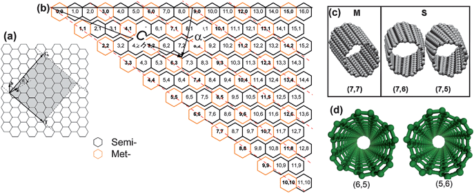 | ||
| Fig. 1 Geometrical structures of SWCNTs. (a) Generation of a carbon nanotube by folding a section of a graphene sheet. The rectangle represents an unrolled unit cell, defined by translation vector T and roll-up vector Ch. (b) Chirality map of SWCNTs, in which the metallic (Met-) and semiconducting (Semi-) SWCNTs are denoted by orange and black hexagons, respectively. The Met-SWCNTs are outlined by the parallel dashed red lines. (c) Examples of Met- and Semi-SWCNTs. (d) Right-handed (6,5) and left-handed (5,6) SWCNTs, which are optical isomers. | ||
Another one is chiral angle θ, the angle between the chiral vector Ch and the a1 direction in the graphene lattice. The chiral vector Ch can be defined by its length and the chiral angle θ. That is, the integers (n,m) of nanotube can alternatively be presented in terms of the diameter dt and chiral angle θ. The nanotube diameter dt can be written in structural indices (n,m) as
| dt = Ch/π = √3aC–C(m2 + mn + n2)1/2/π | (2) |
| θ = tan−1[√3m/(m + 2n)]. | (3) |
Therefore, a nanotube can be specified either by its (n,m) indices or equivalently by dt and θ.15
Among the large number of possible Ch vectors, there are two inequivalent high-symmetry directions, which are termed “armchair” if n equals m (i.e. (n,n)), and “zigzag” in the case that m = 0 (i.e. (n,0)). The axis of the armchair nanotube corresponds to θ = 30°, while the zigzag nanotube axis corresponds to θ = 0°. All other conformations, are known as ‘chiral’ or helical structures. The nanotube axis for chiral nanotubes corresponds to 0° < θ < 30°.
It should be noted that the chiral SWCNTs are optically active. Chiral tubes have two inequivalent helical operations. The tube can be rolled up either above or below the plane of the graphene sheet. These two tubes can be thought of as mirror images of one another, with the graphene sheet defining the mirror plane. That is, one kind of chiral SWCNTs have left-handed (M) and right-handed (P) forms, i.e. SWCNT isomers (Fig. 1d).16,17 For the achiral tubes, this plane is also a reflection plane and the two tubes are identical.
Fig. 1 shows the graphene chirality map of SWCNTs, in which the SWCNTs are labeled according to their chiral indices (n,m). The metallic and semiconducting SWCNTs are marked with orange and black hexagons, respectively. SWCNT isomers with identical chiral vectors but different chiral handedness are not included in Fig. 1b. It can be easily imagined that SWCNTs with similar diameters could include many kinds of the indices, and a small change in the n or m indices could cause striking changes in their electronic properties (Fig. 1b), which make controlled synthesis and extraction of specific tubes from mixtures very challenging. In addition, chiral SWCNT isomers shall have identical chemical properties, resulting in a situation more complicated. Before discussing different separation strategies, basic physical properties of different SWCNTs, as well as the corresponding characterization tools for detection of the nanotube population and species should be understood.
1.2 Electronic properties of SWCNTs
To discuss the electronic properties of SWCNTs, we should first consider the band structure of a layer of graphite (“graphene sheet”).18Fig. 2a and 2b illustrate the band structure of graphene and the hexagonal shape of its first Brillouin zone. The valence π and conduction π* states of graphene are seen to join at six points lying at the Fermi points (i.e. K or KB points), resulting in the graphene acting as a semimetal or zero-gap semiconductor.18,19 In most directions in k-space, such as in the Γ–M direction, the electrons encounter a semiconductor-like band gap. In the Γ–K direction and in five other directions that pass through the Fermi points (K or KB points), the electrons can move freely and the graphene behaves as a metal.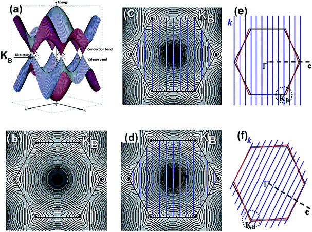 | ||
| Fig. 2 Elelectronic structures of a SWCNT. (a) Three-dimensional plot of the π and π* graphene energy bands and (b) a 2D projection. The hexagon denotes the first Brillouin zone. (c) Allowed 1D wavevectors for a metallic (9,0) SWCNT. (d) Allowed 1D wavevectors for a semiconducting (10,0) tube. The black hexagons define the first Brillouin zone of a graphene sheet, and the black dots in the corners are the KB points. Blue lines represent the allowed wavevectors, k, within the first Brillouin zone. The KB points lie on the dashed lines in metallic carbon nanotubes (c), and lie away from the dashed lines in semiconducting nanotubes (d). The curvature effect on a (9,0) zigzag nanotube (e) and an armchair metallic nanotube (f), under the effect of curvature, KF moves along the circumferential direction away from the KB point in a (9,0) nanotube and along the tube axis in an armchair nanotube (adapted from ref. 19 and ref. 20). | ||
The basic electronic structure and electrical properties of SWCNTs can be deduced from those of graphene.19,20Fig. 2c and 2d shows typical graphene band-structures of a (9,0) and a (10,0) SWCNT. As a finite piece of the 2D graphene sheet is rolled up to form a 1D tube, electrons are confined in the radial direction and can propagate only along the nanotube axis. The accomplished confinement condition (quantization condition), namely, k·Ch = 2πq (where k is the wavevector in the circumferential direction; Ch, the chirality vector; and q, an integer), induces each band of the graphene (σ, σ*, π, π*) to split into a number of one-dimensional (1D) subbands labeled by q. The allowed energy states q of the tube are cuts (indicated by the blue lines) of the graphene band-structure. Therefore, only a particular set of states, which are parallel to the corresponding tube axis with a spacing of 2/dt, are allowed (Fig. 2), so that their wavevectors point to this direction. If one of these subbands passes through one of the K points, the nanotube will be metallic; otherwise it will be semiconducting (Fig. 2c and 2d). Based on the criteria k·Ch = 2πq and unit cell for a (n,m) SWCNT, it can be concluded that SWCNTs are metals when (n − m)/3 is an integer, and are semiconductors otherwise.21,22 That is, based solely on geometry, one-third of the SWCNTs would be metallic and two-thirds semiconducting. SWCNTs are exceptional materials insofar, as they can be metallic or semiconducting although there is no difference in the chemical bonding between the carbon atoms within the tubes and neither doping nor impurities are present.
Several important characteristics of the electronic properties of SWCNTs can be immediately obtained from this π-only tight binding model. First, the spikes shown in the DOS of the SWCNTs, which are called ‘van Hove singularities’ (vHS), define narrow energy ranges where the DOS intensity becomes very large. vHS are theoretically the mirror at the Fermi level and are due to one-dimensional quantum conduction (Fig. 3a), which is not present in an infinite graphite crystal. Second, the DOS at EF is zero for semiconducting SWCNTs (n − m ≠ 3q) but nonzero (albeit small) for metallic SWCNTs (n − m = 3q). Third, the first vHS band gap (E11) for all SWCNTs proportionally depend on the 1/dt, and are independent of chiral angle θ to first order. For most available SWCNTs with a diameter of 0.8–1.5 nm, the semiconducting nanotubes have a band energy ES11 about 0.49–0.92 eV and for metallic nanotubes EM11 are at the range of 1.48–2.77 eV.
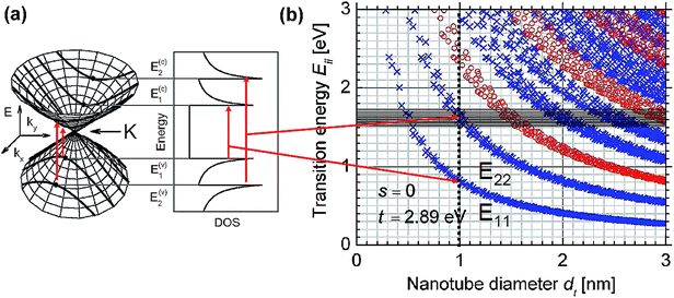 | ||
| Fig. 3 (a) Conical energy bands in the vicinity of the K or named KB points and the translated electronic density of states (DOS). (b) Kataura plot (adapted from ref. 29). | ||
Further tight-binding studies22–24 and low temperature STM experiments25,26 showed that (n,n) tubes are metals, and (n,m) tubes which n − m = 3q (q = integer, q ≠ 0), are very tiny-gap semiconductors, or so-called semimetals.18 The n − m = 3q tubes should all be metals because the allowed wavevector passes through the K point. But because of the tube curvature effects in small-diameter nanotubes, which leads to strong hybridization of the σ/π bonding and σ*/π* antibonding orbitals on carbon,27 it is understood that the K Fermi point (KF) of the graphene band (crossing points for π and π* band) would shift away from the original K point.19,26 For example, the Fermi points of “metallic” zigzag SWCNTs are found to shift away from the K points along the circumference direction, while the Fermi points of armchair SWCNTs shift along the tube axis. Hence, the allowed wavevector in (n,0) and (n,m) metallic tubes no longer passes through the Fermi point, and produces tiny gaps (∼0.05 eV) (so-called semimetal); whereas for (n,n) armchair tubes, they are expected to be truly metallic because the shift occurs along the allowed wavevector and KF remains on the subband of the nanotube. The tiny gap of the semimetals decrease with a 1/dt2 dependence.24,26 However, for most experimentally observed carbon nanotubes (dt > 0.6 nm), the gap in the tiny-gap variety would be so small that their thermal energy is sufficient to excite electrons from the valence to the conduction band.18 So, for the majority of practical purposes, the small band gap in these zigzag and chiral tubes of larger diameter can be effectively considered to be metals at room temperature. Henceforth, the set of tubes with n − m = 3q are referred to as “metallic” to indicate that those with q ≠ 0 have tiny band gaps.26
The metallic SWCNTs have outstanding electron transport properties, such as ballistic transport and very low scattering. Armchair SWCNTs as metals are stable to low temperatures against a spontaneous symmetry breaking and have high carrier mobilities at the Fermi energy (EF), making them outstanding candidates for the ultimate metallic nanowires and components in future logic circuits. The metallic SWCNTs can be used in either flexible transparent electrodes, or electrostatic-proof coatings. Meanwhile, the semiconducting nanotubes are promising for taking the place of silicon in traditional micro-/nano-electronics, such as field effect transistors (FET), thin film transistors (TFT) etc. However, simple metallic or semiconducting nanotubes cannot fully satisfy all these demands of the frontier applications. For example, for semiconduting nanotubes, the (10,5) nanotube has much better performance than others when used in FETs. That is, both the enrichment of metallic or semiconducting tubes, and the purification of single chirallity nanotubes are in high demand.
1.3 Characterization tools
Electronic structure of SWCNTs (Fig. 3) can be observed by various spectroscopic techniques. The most outstanding feature of the electronic interband transitions for SWCNTs is that only the transitions between symmetric vHs are favored, at energies denoted E11, E22, E33, E44…Eii. The preference of the symmetric transitions between vHs resulting in a high efficiency of these characteristic transitions is due to the one dimensional confinement of their electronic structure.28 Therefore, their corresponding optical signals are very strong even at the single tube level. For the characterization of nanotubes via optical spectroscopy, it is very useful to consider the plots of the energies Eiiversus the nanotube diameter dt (so called Kataura plot),29,30 as shown in Fig. 3b. The different energies Eii were calculated based on tight-binding approximations. Each point in this plot represents one optically allowed electronic transition energy (Eii) from a given (n,m) SWCNT. Based on a Kataura plot, several optical methodologies, such as that based on absorption spectroscopy, photoluminescent spectroscopy and scattering resonant spectroscopy, etc., have been utilized to characterize the compositions in various kinds of samples. Recently, circular dichroism (CD) spectroscopy has been established to detect the enrichment of left- or right-handed SWCNTs. These optical techniques are widely available and far from sophisticated. The developments of these diagnostic tools have speeded up the way towards separation of single nanotube species.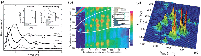 | ||
| Fig. 4 (a) Absorption spectra of different SWCNT sources. The insert one reveals the related electronic transition in met- and semi- SWNTs (adapted from ref. 27). (b) Contour plot of fluorescence intensity versus excitation and emission wavelengths for a sample of surfactant-coated SWCNTs. The insert one depicts the optical excitation and emission transitions of interest (adapted from ref. 49). (c) RBM Raman measurements of HiPco SWNTs dispersed in SDS aqueous solution, measured with 76 different laser lines (adapted from ref. 64). | ||
With a van der Waals binding energy of ∼500 eV/μm for tube-tube contact, the smooth-sided sp2 tubes readily form parallel bundles or ropes.32,33 The bundling perturbs the electronic structure of the tubes, making their absorption peaks red-shifted, superposed and blurred, which destroys the fine structure in the spectra. Moreover, the bundling blocks the selective reaction for inner tubes and thus confounds all attempts to purify the tubes according to size or type, or to use them as individual macromolecular species. Hence, UV-Vis-NIR absorption spectroscopy can be used for studying both the population in the sample or degree of tube bundling of the sample. If one needs to analyze the nanotube distribution via UV-Vis-NIR absorption spectroscopy, the sample must be well dispersed as a solution or thin film.
Optical absorption measurements provide valuable information about the electronic properties of SWCNTs so that they can be used to study covalent or noncovalent interaction between molecules and nanotubes.34–36 When covalent functionalization occurs on nanotubes, the well-resolved absorption peaks weaken and even disappear because the structure of nanotubes partially changes from sp2 hexagonal networks to a sp3 structure. From UV-Vis-NIR absorption spectroscopy, two important issues can be revealed: the extent of the covalent reactions and the selectivity to different nanotubes. Noncovalent doping or molecular adsorptions have the effect of depleting the valence electrons (e.g., p-doping) or saturating the conduction band (e.g., n-doping). These noncovalent interactions could affect the intensity of the absorption peaks. It is worth noting that in terms of doping, electron donors (e.g. K, Cs) or electron acceptors (e.g. I2, Br2)37 show very similar changes in the NIR spectra as both suppress the electronic transitions.38 Adsorbed molecules that cause charge transfer also suppresses NIR E11 absorption,39 while it has been reported that the ES22 band is less sensitive than the ES11 band to the covalent reactions, noncovalent adsorption or doping.
Absorption spectroscopy has been widely used to estimate the abundance of metallic or semiconducting components by comparing the intensities of each component, since these resonant peak positions are chirality- and diameter- dependent. For qualitative analysis, absorption spectroscopy is excellent in getting a full view of the sample composition. However, a real quantitative evaluation is not straightforward due to several practical reasons. Firstly, absorption matrix elements of nanotubes are dependent on (n,m).40 It has been reported that the extinction coefficient ratio for metallic to semiconducting SWCNTs is of 0.352 ± 0.009, which should be independent of the separation method or starting materials used.8 However, the data for the extinction coefficients of different SWCNTs are limited and inconsistent in the literature, and better measurements on the extinction coefficient variation for different (n,m) nanotubes are still necessary.41 Secondly, the strong π plasmon absorption in the short wavelength region makes the resonant transition indistinct. Some nanotube samples in fact contain a lot of contaminations (typically polyhedral graphitic particles, amorphous carbon, catalyst particles, etc.). The optical absorption of these contaminations also contributes to the spectral background, which inevitably introduces errors in the quantitative evaluation when one tries to perform background subtraction. The third difficulty in measuring the SWCNT concentration arises from the dispersants that are usually introduced during the dispersion process, which may mislead the assessment of the SWCNT concentration in a solvent. Moreover, the numeric deconvolution of the overlapped peaks are always complicated.42,43 10–20% error is estimated arising from the extinction coefficients difference among different SWCNTs and the presence of baseline and phonon side-bands near E11 peaks.31 In conclusion, the presence of a large number of different (n,m) SWCNTs with unknown abundance along with various errors associated with data analysis44 make the quantitative evaluation of the concentration of specific (n,m) species in sample very challenging. Under these circumstances, only a few estimation procedures from absorption data have been established after corroboration and these can be applied in semiquantitative abundance evaluation.42,45,46
Continuous PL excitation measurements resulted in the precise mapping of the transition energies for various semiconducting species (Fig. 4b). The nanotube structure (diameter and chiral angle) controls the intrinsic electronic and vibrational properties of pristine nanotubes, leading to structure-dependent variations in fluorescence. Fluorimetry readily provides qualitative analysis, i.e. identifying semiconducting (n,m) species through their assigned absorption and emission wavelengths. However, tube indices can not be accurately deduced simply from excitation and emission peak position since the PL position of nanotubes are sensitive to the “micelle” environment. Red shifts or blue shifts and different PL efficiencies due to their degree of dispersion statement are observed in the samples suspended by the assistantance of different reagents.48 Bachilo et al. have illustrated a brief principle with three steps on deducing the assignment of (n,m) nanotube in excitation-emission matrix.49
Quantitative evaluation of nanotube abundances requires knowledge of the structure-dependent factors that connect observed fluorimetric intensities to the actual species concentrations.50 The PL intensities have been calculated by multiplying the photon-absorption, phonon-relaxation and photon-emission matrix elements. Among them, photon-absorption and photonemission matrix elements show family patterns,47,49 that is the fluorescence efficiencies depend on the family pattern (i.e. 2n + m = constant). Bachilo et al.49 and Oyama et al.47 have revealed the family behavior and quantum efficiency for most (n,m) nanotubes from both theoretical calculation and experiments. The E22/E11 ratio in the PL spectrum provides important information on the (n,m) index, i.e. tube's family pattern. Nanotubes with smaller θ possess weaker PL intensities than those with higher θ, as suggested from both theoretical and experimental studies. Moreover, the quantum efficiencies of (n,m) nanotubes are different according to modality and diameter and thus further complicates (n,m) abundance evaluation. The exterior factors influencing the fluorimetric intensity include all nonideal factors, such as finite length, growth defects, aggregation and other environmental irregularities, physical or chemical damage, and chemical functionalization. Interaction between the covalent or noncovalent guest molecules with host nanotubes can lead to either enhancement51 or quenching34,52 of the PL intensities.
However, the fluorescence intensity is proportional to the concentration of a species, and therefore quantitative analysis via fluorimetry has been utilized on the abundances of species in a bulk sample and separation efficiency for certain (n,m) nanotubes can be assessed.47,53 Much effort have been devoted to construct and simplify the evaluation methods for the distribution of each (n,m) nanotube in the sample. A simple derivative method by Arnold et al. has been applied for estimating the relative concentration of (n,m) nanotubes.45 However, considerable estimation error is also introduced by not considering the difference of quantum yield of (n,m) nanotubes.47,50,53 The relative quantum efficiencies of semiconducting species have been widely investigated to benefit the evaluation of relative (n,m) concentration in the sample. Jorio53 and Oyama47 calculated the quantum yield of most (n,m) nanotubes. Experimentally, Tsyboulski et al.50 have developed empirical calibration factors from fluorescence of individual nanotubes on a substrate for most semiconducting species, which currently provide the most reliable and comprehensive calibration factors in estimating the (n,m) distributions based on bulk PL intensities.
The PL intensity is proportional to a tube's luminescence quantum yield, i.e. photon-emission matrix elements.50 The absolute luminescence quantum yield has been found by comparing the measured luminescence intensity and absorbance with that of a solution of known quantum yield. Semiconducting nanotubes have weak ensemble luminescence quantum yields at ∼1%.33 Possible causes include intrinsic low-lying, nonradiative states (dark excitons) and various nonideal exterior influences mentioned above.54 The exterior factors make the detected quantum efficiencies vary from 0.1% for surfactant-micellarized nanotubes,33 and 1.5% for polyfluorene wrapped SWCNTs,55 to 8% for individual SWCNTs on substrate.50 Recently, the PL of semiconducting nanotubes was greatly brightened via an oxygen-excluding surfactant organization, which led to quantum yields as high as 20%.54 It is deemed that oxygen can quench PL through hole doping and subsequent nonradiative Auger recombination.56
In summary, PL spectroscopy provides a quick and practical spectroscopic route for finding the detailed composition of semiconducting SWCNTs in the bulk samples. It is advantageous on identification for almost all semiconducting (n,m) SWCNTs. This method can be adapted for rapid analysis to guide the processes that selectively produce or sort nanotubes by structure.55,57 However, considering that the many nonideal (extrinsic) factors as well as the suppression effect of these nonideal factors may vary with the (n,m) index, further research is needed to explore such structure dependence of the extrinsic quenching in nanotubes and to devise standard ways to minimize or compensate for them. The nanotube dispersion (one of extrinsic factors) and examination process are required to be normalized firstly. At present, it is suggested that the empirical quantitative results (intrinsic action cross sections) described in ref. 42 might be applied as provisional calibration factors to estimate (n,m) distributions.
For the characterization of nanotubes by Raman spectroscopy, it is very useful to consider Kataura plots (Fig. 3b). This plot should be considered as a guide for answering the question “which (n,m) carbon nanotubes are in resonance with a given Elaser?”58 Each point in this plot represents one optically allowed electronic transition energy (Eii) from a given (n,m) SWCNT. The SWCNTs which are predicted to be resonant must have Eii within a resonant window Elaser ± 0.10 eV. Then the resonant nanotubes in the sample can be deduced from the RRS.
The main Raman characteristics of SWCNTs include the radial breathing mode (RBM), tangential mode (G band), disorder-induced mode (D band) and its second-order harmonic (G′ band).59 The RBM Raman features, appearing between 100 cm−1 < ωRBM < 300 cm−1 for SWCNTs within 0.75 nm < dt < 2.4 nm (Fig. 4c), correspond to symmetric in-phase displacements of all the carbon atoms in the SWCNT in the radial direction, as if the tube is breathing. The tangential G band is derived from neighboring atoms moving in opposite directions along the surface of the tube as in 2D graphite, which gives characteristic multi-peak features around 1500–1600 cm−1. Neither the RBM feature nor the multi-component G band features are observed in any other sp2 bonded carbon material. Typically, sp2 bonded carbon materials show a characteristic single G band (Lorentzian shape) Raman peak at about 1582 cm−1. The disorder-induced D band is only activated in the Raman spectrum of sp2 carbons in the presence of hetero-atoms, vacancies, or any defect.60 All features of these Raman spectra are sensitive to nanotube structure (n,m indices).58,61 However, the RBM is most sensitive, therefore is used to make the initial (n,m) identification. The G band is very sensitive to the electronic properties as well. The RBM and G band have been widely used to characterize the efficiency in sorting nanotubes.
The low-frequency RBM feature provides a convenient method for the determination of both dt and Eii from the Kataura plot. The frequency of RBM ωRBM is related to the nanotube diameter by ωRBM ∝ 1/dt according to the relation ωRBM = A/dt + B and independent of chiral angle θ.62 A large number of different constant values for A and B in above relation result from experiments and ab initio calculations that have been reported in the literature. However, the relation between ωRBM and dt can be converged to eqn (4) considering the van der Waals interaction with the environment.63
 | (4) |
The parameter Ce in eqn (4) describes environmental effects with values ranging from 0.05 to 0.07 by fitting the RBM results in the literature. Under the Elaser energy (which means the transition energy Eii), the yielded dt (according the above relation from ωRBM) can identify the index i in Eii and further to determine the (n,m). It is clear that a single laser Raman measurement only gives an idea of the tubes that are in resonance with that laser energy, but does not give a complete characterization of the sample, such as (n,m) or diameter distribution. In practice, tunable laser systems were applied to Raman spectroscopy studies of nanotube and the (n,m) determination could then be made more accurate and comprehensive (Fig. 4c). By taking Raman spectra under many laser lines, a good characterization of the diameter distribution as well as metallic/semiconducting population in the sample can be obtained.62,64
It has been confirmed that there are characteristic differences between the G bands for metallic and semiconducting nanotubes.29,65 In graphite the G feature has a single peak since in-plane tangential vibrations are degenerate in the hexagonal sheet; while in nanotubes, this feature splits into up to six peaks due to the curvature of the graphene sheet and the quantum confinement along the tube circumference.59 A simple analysis can be carried out only considering the two most intense peaks, which basically originate from the symmetry breaking of the tangential vibration when the graphene sheet is rolled to make a cylindrically shaped tube. The two most intense G peaks are labeled by G+, for atomic displacements along the tube axis, and G− with lower frequency, for modes with atomic displacement along the circumferential direction.11 The difference between the G bands of semiconducting and metallic SWCNTs is evident in the lineshape of the G− feature. The G− feature of metallic tubes is broader, more asymmetric, and is downshifted in frequency compared with the semiconducting tubes. This asymmetric broadened G− feature is usually fitted using a Breit–Wigner–Fano (BWF) lineshape that accounts for the presence of free electrons in nanotubes with metallic character,29 while the G bands of semiconducting tubes all feature a Lorentzian lineshape. This BWF line was also observed in other graphite-like materials with metallic character, such as n-doped graphite intercalation compounds, n-doped fullerenes, and metallic impurities.58,66 These findings are important for using the Raman spectra to distinguish between metallic and semiconducting tubes.
Using Raman spectroscopy for the comparative and qualitative analysis of nanotube composition can be easily performed on most type of samples. But for an absolute (n,m) abundance assignment, the resonance Raman cross section dependence on (n,m) has to be established at first. It has been reported that the Raman scattering cross section depends on nanotube's diameter and chiral angle.49,67 These parameters change the Raman intensities by about one order of magnitude, and such effects have also been observed experimentally.28
Among all the above characterization techniques, NIR absorption, PL and RSS are the most useful tools in nanotube identification. These three spectroscopic tools are highly sensitive, along with advantages such as non-invasive, non-contact, and readily available probes. However, each tool has its drawbacks. It should be noted that PL can only characterize semiconducting SWCNTs. RRS can measure both semiconducting and metallic SWCNTs, while it's still not easy to achieve a full assessment of the whole sample. Vis-NIR absorption spectrometry has the advantage of presenting all (n,m) tubes in the sample in one spectrum, that is a full-scale evaluation of the sample at one glance, but in return it lacks resolution for bulk sample with various (n,m) tubes. Whereas, the 2D or 3D plots of PL and/or RRS spectroscopy allow much better discrimination of each species with the discrete characteristic (n,m) peaks. To the above characteristic tools, there have many questions to answer before they can be used for exact quantitative analysis, such as the (n,m) depenence of matrix elements for these optical behaviors, and resonant factors, extinction coefficiencies, quantum efficiency for most (n,m) tubes. To date, comparisons between these different quantitatively characteristic tools are rarely reported, and to establish a standard quantitative measurement procedure is still a task yet to be accomplished.
2. Separation of SWCNTs via covalent approaches
2.1 Side-wall functionalization
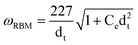
Carbon nanotubes are of cylinder structure with sp2 hybridized carbon bonds. The reactivity of carbon nanotube is thus directly related to the mismatch of π-orbital caused by curvature. A higher reactivity for smaller diameter carbon nanotubes towards the addition reactions can be attributed to the increased steric strain.27,72 Moreover, the selective electrophilic addition reactions on SWCNTs could be understood by terms familiar to chemists: a higher reactivity for metallic nanotubes is expected due to their higher HOMO level.73 The selectivity in sidewall functionalization reactions can also be understood in terms of the electronic density of states (DOS) as shown in Fig. 5. Metallic SWCNTs, contrary to semiconducting SWCNTs, have finite electron DOS at their Fermi levels (The Fermi level is the chemical potential of the electrons. In metals it is the topmost filled level at zero temperature, while in semiconductors it lies within the band gap, where no states are allowed.) Hence there are electrons available to stabilize the charge-transfer complex presumably formed by the addition reagent at the nanotube surface.74 Metallic SWCNTs thus are better to stabilize the transition state and may consequentially accelerate the forward rate of reaction. This could be the reason for that almost all of the reported electrophilic addition reactions have a reactivity on the metallic SWCNTs, such as [2 + 1] (dicholrocarbene and carbene addition), [2 + 3] (diazonium ion reaction, and osmylation), [2 + 2] (fluorinated olefins) cycloaddition, and hydrosilylation addition.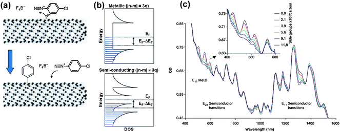 | ||
| Fig. 5 Diazonium reagents functionalize SWCNTs with selectivity towards metallic SWCNTs and enable manipulation according to the SWCNT electronic structure. (a) Schematic illustration of the diazonium functionalization. (b) Supposed mechanism of the selectivity towards metallic SWCNTs. (c) The alternation of UV-Vis-NIR absorption spectrum with the addition of various amounts of diazonium reagents (adapted from ref. 34). | ||
The reactions of SWCNTs with diazonium salts/ions have been intensively investigated since the water soluble aryl diazonium reagents first showed selective reaction on metallic SWCNTs in aqueous solution.34 The diazonium salts have been introduced to convert metallic SWCNTs into semiconducting type by forming a covalent aryl bond on the nanotube (shown in Fig. 5), while thermal annealing of the diazonium-treated nanotubes cleaved the aryl moieties from the sidewalls and recovered the metallic nanotubes.34,36,75 Soon thereafter, this chemistry has also been used to render metallic SWCNTs inactive in thin-film electronic devices and single tube devices, because diazonium covalent functionalization significantly perturbs the electronic and optical properties of metallic SWCNTs. An,76 Wang,77 and Balasubramanian78 studied the selectivity of this reaction directly on network-type nanotube FETs in order to fabricate all-semiconductor-behaving nanotube devices. They have found that the concentration of the diazonium reagents play an important role in the selectivity of the reaction and thus in the performance of the FETs. It was revealed that a significant suppression of the metallic tube conductivity requires concentrations at which considerable reaction also occurs for most semiconducting tubes,77 which explain the observation that covalent functionalization gave limited improvement in SWCNT FETs performance. Further investigations on the optimization of this reaction were carried out. Different p-substituted benzenediazonium salts have been explored recently,79–81 and a higher selectivity of NO2-phenyl functionalization on metallic SWCNTs was observed,79,81 while the Cl-phenyl functionalization was more sensitive to the nanotube diameter.79 Mechanism studies of the diazonium reaction on nanotubes have revealed a free-radical chain mechanism, which suggested that the selectivity of the reaction can be improved by optimizing the electrophilicity of the aryl radical.81 This allows opportunities to further tune the metallic/semiconducting SWCNT selectivity. It should also be mentioned that after functionalizing with a p-hydroxybenzene diazonium salt, a negative charge can be selectively introduced on the metallic SWCNTs through deprotonation in alkaline solutions, thus enabling subsequent separation using free solution electrophoresis.75
Treating the SWCNTs with dichlorocarbene82 was reported to convert metallic nanotubes into semiconducting ones. This result was supported by a strong decrease in intensity in the far-infrared absorption spectrum, assigned to pseudo gap near the Fermi level of metallic tube, and a simultaneous intensity increase in the visible-NIR region corresponding to the absorption of semiconducting nanotubes. The interaction of osmium tetroxide (OsO4) with SWCNTs in the presence of UV irradiation showed chemical specificity for metallic nanotubes.83 The result of this osmylation is the covalent sidewall functionalization of these nanotubes through disruption of the sp2 structure, as well as a reduction of the OsO4 species to OsO2 nanoparticles, which were then adsorbed onto the sidewall surface. The Raman study of the nanotube samples showed some evidence of a higher reactivity of metallic tubes.
Selective covalent sidewall functionalization of semiconducting SWCNTs also have been achieved by 1,3-dipolar cycloaddition of azomethineylides derived from trialklyamine-N oxides labeled with polycyclic aromatics,84 in which process metallic nanotubes can be enriched in the precipitate sample. Theoretical studies have suggested that this 1,3-dipolar cycloaddition was sensitive to the diameter and chirality of nanotubes.85
Recently, two highly selective reactions have been reported. A [2 + 2] cycloaddition reaction was shown to suppress heavily the metallic conductivity in thin-film transistors (TFTs).86 The cycloaddition of fluorinated olefin reagents preferentially reacted with metallic nanotubes, and the fluorinated ethylene substitute affected the performance of the TFTs. It was suggested that 1 carbon atom–0.018 fluorinated ethylene reagent level was sufficient to achieve the complete conversion of the metallic tubes without degrading the semiconducting tubes. TFTs using these functionalized SWCNTs as the semiconducting layer gave mobilities of 100 cm2 V−1 s and on/off ratios of 105. Lee et al. have illustrated that a hydrosilylation reaction occurred spontaneously on small-diameter metallic SWCNTs at room temperature.87 This reaction was simply performed by adding SWCNT-containing substrates into the triethylsilane hexane (or silane compounds containing a neutral Si–Hx moiety) solution in an N2 protective atmosphere for 1 h at room temperature. The successful formation of a covalent bond on metallic nanotubes was detected by AFM-correlated nano-Raman spectroscopy. The hydrosilylation reaction was successfully applied to network-type SWCNT-FET devices to selectively silence metallic SWCNTs. The resulted FET devices showed dramatically increased on/off current ratios.
2.2 Selective destruction
In general, selective covalent chemistry on metallic nanotubes can be classified into two categories according to the extent of reactions: one is converting metallic nanotubes to the semiconducting type, that is silencing the metallic one; another is eliminating metallic nanotubes. The former reaction is concomitant with electronic localization and loss of translational symmetry, and opens a gap at the Fermi level of the metallic nanotubes. The latter one breaks up the all-conjugated system into a series of smaller aromatic pieces by opening C–C bonds in the nanotube backbone. The final results of both kinds are that the semiconducting behaved SWCNTs dominate the performance of the nanoelectronic devices. Nevertheless, it should be noted that in regard to covalent selective reactions, concentration control of the reactive reagents is always important. Many researchers suggest that when the concentration was relatively high, both types of nanotubes are disturbed. Taking FETs for example, over reaction largely decreases the off current and thus increases the on/off ratio to over 105. On the other hand, vigorous reaction always destroys the extra high mobility, which is another important parameter for electronic devices. Therefore, there is a balance between the extent of the reaction and final performance of devices. Though covalent chemistry can be conducted in situ on devices and can be scaled up, there are several flaws for covalent approaches. First of all, most tubes are inevitably functionalized and hence the electronic structures of the SWCNTs are disturbed because of the defects. Secondly, intensive reaction arouses the subsequent problem of purification for the nanotube fragment and amorphous carbon. Most importantly, so far there is no covalent reaction that can be used to achieve the purification of a single species of (n,m) nanotubes.
3. Separation of SWCNTs via non-covalent approaches
Another strategy for SWCNT separation, which is based on the selective dispersion of noncovalently modified SWCNTs in solutions, is currently being pursued in an effort to minimize perturbation to the SWCNT structures. Noncovalent approaches have the advantage of simplicity, less destructive and preserving the intrinsic electronic properties of nanotubes. Furthermore, they have been utilized in extracting single (n,m) tube species. The key to the noncovalent strategy is to find the appropriate dispersing reagents that could discriminate between different SWCNTs in accordance to their diameter or chirality. A variety of small molecules and macromolecules have been explored for this purpose. In the following part, we will discuss the various nanocovalent separation approaches from two aspects, the dispersing reagents and the separation techniques.3.1 Dispersing reagents
DNA has been extensively investigated in extracting particular nanotubes via noncovalent wrapping. Single stranded DNA was firstly utilized to disperse nanotubes by Zheng and coworkers in 2003.105 They found that whether DNA wrapping is selective depends on the specific sequence of the DNA strand. It was reported that an oligonucleotide sequence poly(GT) self-assembled into a highly ordered structure on SWCNTs, allowing metallic/semiconducting tube separation and diameter-dependent separation.106 The DNA wraps on an individual tube in such a way that the electrostatics of the DNA–SWCNT hybrid depends on tube diameter and electronic properties, enabling nanotube separation by conventional ion-exchange chromatography (IEX). Optical absorption and Raman spectroscopy showed that the early fractions were enriched by the smaller diameter and metallic nanotubes, whereas the later fractions were enriched by the larger diameter and semiconducting tubes.106
Since then, a lot of effort has been devoted to studying the interaction between DNA and nanotubes.107–109 Kim et al. have described a solubilization separation method using genomic DNA to exfoliate and disperse nanotubes, which resulted in selectively enrichment of (6,5) nanotubes as compared to (10,3) tubes.110 Enrichment of metallic tubes becomes more effective as the length of DNA decreases. Recently, a breakthrough on separation/purification of single species nanotube has been made by Zheng's group using DNA wrapping combined with size exclusion chromatography (SEC) and IEX separation.31,111 They have tested more than 20 short DNA sequences, and each sequence recognized a particular nanotube species from the synthetic mixture and enabled chromatographic purification. Twelve major single-chirality semiconducting species from a synthetic mixture were extracted with very high purity.31 Purification of each and every single-chirality species from the synthetic mixture of SWCNTs has been proven not to be insurmountable to date. Conceptually different from the extensively discussed binding affinity, it is believed that the structural order of a DNA–SWCNT hybrid provides the structural recognition of SWCNTs (Fig. 6b and 6c). Theoretical simulation revealed that recognition sequences exhibited a periodic purine–pyrimidine pattern, which could undergo hydrogen-bonding to form a two-dimensional sheet, and fold selectively on nanotubes into a well-ordered three-dimensional barrel.31,112 The extracted (10,5) tubes, the largest one among the 12 species, was obtained through the ssDNA sequence (TTTA)3T, and these tubes performed excellently when they were applied in FET devices (Fig. 6).9 This sample gave a single species signal under all the spectroscopic characterizations, confirming that it contained nearly pure (10,5) SWCNTs. According to the electrical measurements the purity was 99%. Half of the FETs composed of the separated SWCNTs in parallel gave an on/off ratio greater than 106 and around 88% of the devices exhibited on/off ratio >102. So far, this is the first time that so many (n,m) species could be separated with extremely high purity. However, the obstacles in scale-up are still tremendous, which have been discussed in a review from Tu and Zheng.109 It is so far one of the most promising approaches and so-called experimental tour de force to achieve high purity nanotubes with single species.
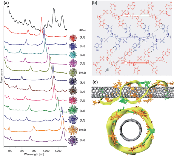 | ||
| Fig. 6 (a) Optical absorption spectra of the starting HiPco mixture and 12 purified semi- SWCNTs extracted via specialized DNA wrapping. The structures of 12 semi-SWCNTs are given at the side of spectra. (b) A 2D DNA sheet structure formed by three antiparallel DNA single strands through hydrogen bonds and their wrapping direction on SWCNTs. (c) Side view and front view of the 2D DNA sheet wrapped on a (8,4) nanotube, which forms a DNA barrel on nanotube (adapted from ref. 31). | ||
Various surfactants have been studied to sort out SWCNTs according to their chiralities. Doorn et al. reported the selective aggregation of SWCNTs via salt-added SDS solution.35 Diameter and chirality-dependent binding have been observed for common surfactants (for example, sodium dodecyl sulfate, sodium dodecylbenzene sulfonate, and sodium cholate) in aqueous solution. McDonald et al. demonstrated that SDS has a stronger binding to smaller-diameter nanotubes.116 Arnold et al. showed the metal/semiconductor separation and single species separation of SWCNTs via density gradient centrifugation (DGC) by the assistant dispersion of two competing surfactants.45 Wei et al. achieved selective enrichment of (6,5) and (8,3) SWCNTs to purities of more than 85% using SDS and SC cosurfactants via only a dispersion-centrifugation process.117 This means that surfactants, especially co-surfactants, do have selectivity on the electronic type or chirality of SWCNTs. Moshammer confirmed that the SDS has discrimination of nanotubes' electronic types.118 After centrifugation, the supernatant of SDS dispersed SWCNTs/D2O suspension contained semiconducting SWCNTs primarily in the form of small but long bundles, whereas metallic SWCNTs are predominantly suspended as short individual tubes. This difference can be enlarged by the subsequent DGC or agarose gel electrophoresis. Tanaka and coworkers found that both the dispersion surfactant and agarose gel were important to the final separation efficiencies.119 They developed a very simple and scalable gel method to separate metallic and semiconducting nanotubes both with high purity. Whether the agarose gel plays an initial role of the discrimination (i.e. affinity between agarose gel and semiconducting SWCNTs) needs further investigation.
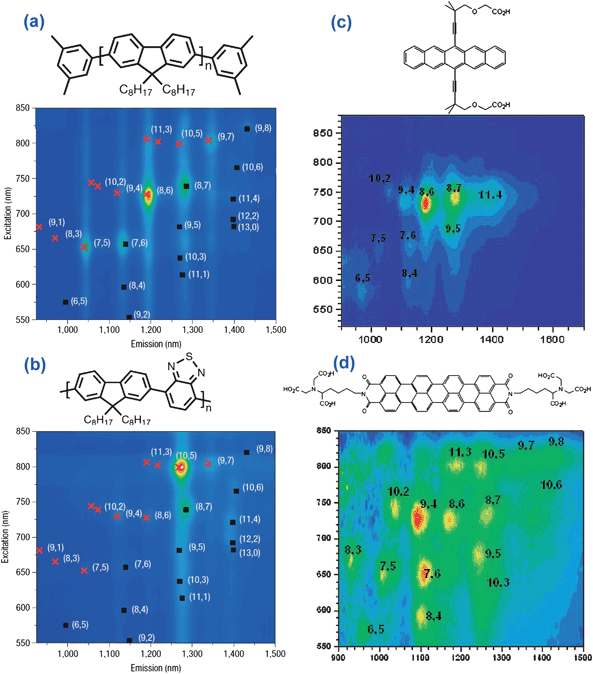 | ||
| Fig. 7 Aromatic molecular structures and their corresponding discriminative behavior on attaching to the sidewall of SWCNTs. (a) and (b) illustrate aromatic polyfluorene derivatives and corresponding fluorescence plots of the extracted SWCNTs (adapted from ref. 55), (c) and (d) show condensed benzenoid aromatics extracting nanotubes according to tube chirality (adapted from ref. 124). | ||
Very recently, Komatsu's group has made a breakthrough in the separation of optical isomers of nanotubes using chiral diporphyrin aromatic molecules (Fig. 8).71,128 The chiral diporphyrin isomers acted as molecular tweezers to preferentially extract either right- or left- handed SWCNTs. The degree of chiral selectivity can be optimized by controlling the dihedral angle between the porphyrins.17 It is amazing that the diporphyrin molecules can read the handedness of the carbon lattice in space. Prior to this work, only aberration-corrected electron diffraction or scanning tunnelling microscopy could come close to identifying SWCNT enantiomers. To some extent, this work inspires the researchers with more confidence in the separation of chiral nanotubes.
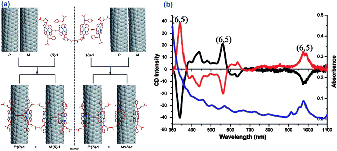 | ||
| Fig. 8 Modeling and experimental results of chiral nanotweezer molecules extracted left-hand (M) and/or right-handed (P) SWCNTs. (a) From the change of enthalpy of the system after the formation of complex structure, the more stable complexes were shown. (b) Circular dichroism spectra of the enriched M- and/or P- SWCNTs (adapted from ref. 17). | ||
The superiority of using aromatic molecules is their structural variety and similarity with nanotubes. Molecules can be designed and synthesized to match the requirements for the separation. Generally, two criteria are required to achieve the noncovalent separation: one is a discriminative adsorption by molecules; and the other is the adsorption enhanced dispersion of SWCNTs.125 Hence, solvents always affect the separation efficiency in these noncovalent approaches.
3.2 Separation techniques
A variety of techniques have been explored in the researches of SWCNT separation, and the most widely used are liquid chromatography, electrophoresis or dielectrophoresis, centrifugation and density gradient centrifugation (DGC) methods.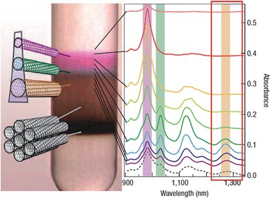 | ||
| Fig. 9 Sorting of SWCNTs by diameter, band gap and electronic type using density gradient ultracentrifugation (adapted from ref. 45). | ||
Recently, Tanaka et al. established a very simple, rapid and scalable gel approach to separate met-/semi- nanotubes with high purity (shown in Fig. 10).119 In their work, a piece of agarose gel containing SWCNTs and SDS was frozen, thawed, and then squeezed. This simple process afforded a solution containing 70% pure metallic SWCNTs and leaves a gel containing 95% pure semiconducting SWCNTs. This gel-based separation method has profound potential for the industrial production of metallic and semiconducting SWCNTs.
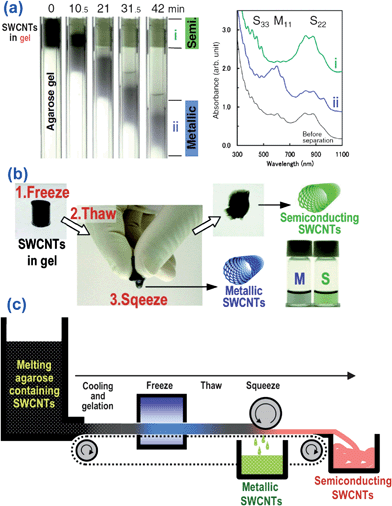 | ||
| Fig. 10 (a) Separation of the SWCNT-dispersed solution by agarose gel electrophoresis (AGE). Sequential photographs show the progress of separation. Absorption spectra of fractions after AGE and absorption spectra indicate the purities of the separated fractions. (b) Met-/Semi- separation by the freeze and squeeze method. Frozen agarose gel containing SWCNTs dispersed with SDS is thawed and squeezed by hand. (c) Illustration of continuous Met-/Semi- separation by the freeze and squeeze method (adapted from ref. 119). | ||
In principle, the separation efficiency may be improved if the above mentioned separation processes could be repeated or combined. Owning to the apparent simplicity, the gel-based separation processes are mostly likely to be cycled to achieve high separation efficiency while giving acceptable yield. Progresses in this direction are anticipated in the near future.
4. Controlled growth
To enable future SWCNT-based molecular device applications, exhaustive efforts have been made on selective synthesis, which is essential to obtain nanotubes with identical properties. Two catalyst systems, Co-MCM-41136 and Co–Mo,137,138 have been demonstrated to produce narrow (n,m)- distributed SWCNTs in carbon monoxide CVD (but still produce ∼20 different (n,m) nanotubes).43 The bimetallic FeRu catalyst was found to grow narrow (n,m)-distributed SWCNTs with small diameter (<1.2 nm) in methane CVD.139 Examples of enriched semiconductor SWCNT growth via plasma enhanced chemical vapor deposition have been reported.140 A 96% semiconducting SWCNT sample was obtained using combined PECVD and fast heating.141 Wang et al. have reported an enriched metallic SWCNT growth process via pyrolysis of a monohydroxy alcohol homologue carbon feedstock on a Fe–Co/MgO catalyst.142 They claimed that the produced SWCNTs contain as high as 65% metallic nanotubes. Harutyunyan et al. grew SWNTs from Fe nanocatalysts and in situ annealed in a He or Ar ambient that contains various ratios of H2 and H2O. They altered the fraction of tubes with metallic conductivity to a maximum of 91% based on Raman spectroscopy and electronic FET tests.143 Most of the selective synthesis processes reported to date yield one or two major SWCNT species in around 20–30% abundance, along with many other minor species of similar diameter.136,137,139Another interesting strategy is to synthesis fundamental units of a specific chirality using organic synthetic methods. Bertozzi et al. have synthesized the shortest possible slice of an armchair carbon nanotube, a structure they refer to as ‘carbon nanohoops’.144 Scott et al. tried to synthesize nanotube fractions via Diels–Alder cycloaddition reactions.145 However, these synthetic strategy are too laborious for commercial applications at the moment.
A more economically attractive option to scale up single species nanotubes may be to use high purity SWCNT “seeds” as templates for synthetic growth of the same chirality tubes.146 This recently demonstrated “cloning” concept147 may help to realize the dream of synthesizing single species SWCNTs. However, great efforts are needed for the cloning approach to increase yield and coinstantaneously keep the coherent chirality.
5. Conclusions and outlooks
In the past decade, we have witnessed remarkable progress chirality in the field of designing different strategies for separating SWCNTs via different chemical methods. Several chemical post-synthetic approaches have given exciting advances on diameter-selective separation, metallic/semiconducting nanotube separation and optical isomer separation.There have been two interlaced development lines for the chemical post-synthetic strategies. The first strategy is based on selective reactions, which seem to be relatively simple and easy for scale up. However, the purity of the product is not sufficiently high at the moment, and the intrinsic properties of the SWCNTs tend to be modified by the chemical reactions. The other strategy is based on preferential attachments of functional moieties onto a particular species of nanotube via noncovalent interactions. Efficient sorting of the SWCNTs can then be subsequently carried out through a number of separation techniques. The purification of single (n,m) nanotube species has been successfully achieved by several methods based on this type of strategy. However, these separation methods are still facing many obstacles in scaling up, such as selectivity to different (n,m) species, effectiveness in working with bulk materials, and adaptability for SWCNTs from different sources.
So far, the reported selective synthetic methods have not shown the degree of control as good as that of the available post-synthetic approaches. The recently reported “cloning” growth is promising in producing identical SWCNTs, but the efficiency needs further improvement. The combination of selective growth approaches with post-synthetic strategies may well be the most economic and feasible way for scale-up purposes.
It is also clear that characterization techniques and tools will need to be constantly refined and improved upon in order to yield quantitative data, which can more definitively determine the viability and efficiency of new approaches towards achieving specific nanotubes.
Though it is still early to predict when the scalable procedures for producing single species SWCNTs with high purity can be eventually developed, the solutions to many technical problems are still needed before the selective separation or controlled growth can match the requirements of real-world applications. The efforts toward this direction have already resulted in significant developments in new science and technology. More breakthroughs and exciting findings are anticipated along with further research in this field.
Acknowledgements
The authors are grateful to the financial support from the National Natural Science Foundation of China (NSFC. 21073079, J0730429), National Lab of Vacuum & Cryogenics Technology and Physics (5145020105JW2301), Chunhui project and “111” project. Proofreading by Dr Sean H. Zhang is also acknowledged.References
- S. Iijima, Nature, 1991, 354, 56–58 CrossRef CAS; S. Iijima and T. Ichihashi, Nature, 1993, 363, 603–605 CrossRef CAS.
- S. Subramoney, Adv. Mater., 1998, 10, 1157–1158 CrossRef CAS; P. G. Collins and P. Avouris, Sci. Am., 2000, 283, 62–69 CrossRef CAS; R. H. Baughman, A. A. Zakhidov and W. A. de Heer, Science, 2002, 297, 787–792 CrossRef CAS.
- P. J. F. Harris, Carbon Nanotubes and Related Structures: New Materials for the Twenty-First Century, Cambridge University Press, 1999 Search PubMed.
- M. Terrones, Int. Mater. Rev., 2004, 49, 325–377 Search PubMed.
- R. Andrews, D. Jacques, D. L. Qian and T. Rantell, Acc. Chem. Res., 2002, 35, 1008–1017 CrossRef CAS.
- M. Knupfer, Surf. Sci. Rep., 2001, 42, 1–74 CrossRef CAS; S. G. Louie, in Carbon Nanotubes – Synthesis, Structure, Properties, and Applications, ed. M. S. Dresselhaus, G. Dresselhaus, P. Avouris. springer, 2001, vol. 80, pp. 113–145 Search PubMed.
- O. Teri Wang, H. Jin-Lin and Charles M. Lieber, Ann. N.Y. Acad. Sci., 2002, 960, 203–215.
- W.-J. Kim, C. Y. Lee, K. P. O'brien, J. J. Plombon, J. M. Blackwell and M. S. Strano, J. Am. Chem. Soc., 2009, 131, 3128–3129 CrossRef CAS.
- L. Zhang, X. Tu, K. Welsher, X. Wang, M. Zheng and H. Dai, J. Am. Chem. Soc., 2009, 131, 2454–2455 CrossRef CAS.
- S. Banerjee, T. Hemraj-Benny and S. S. Wong, J. Nanosci. Nanotechnol., 2005, 5, 841–855 CrossRef CAS.
- R. Krupke, F. Hennrich, H. von Lohneysen and M. M. Kappes, Science, 2003, 301, 344–347 CrossRef CAS.
- P. C. Collins, M. S. Arnold and P. Avouris, Science, 2001, 292, 706–709 CrossRef.
- R. B. Weisman, Nat. Mater., 2003, 2, 569–570 CrossRef CAS; S. Campidelli, M. Meneghetti and M. Prato, Small, 2007, 3, 1672–1676 CrossRef CAS; M. C. Hersam, Nat. Nanotechnol., 2008, 3, 387–394 CrossRef.
- M. S. Dresselhaus, G. Dresselhaus and R. Saito, Phys. Rev. B: Condens. Matter, 1992, 45, 6234 CrossRef CAS.
- M. S. Dresselhaus, G. Dresselhaus and A. Jorio, Annu. Rev. Mater. Res., 2004, 34, 247–278 CrossRef CAS.
- M. S. Strano, Nat. Nanotechnol., 2007, 2, 340–341 CrossRef CAS.
- X. B. Peng, N. Komatsu, T. Kimura and A. Osuka, J. Am. Chem. Soc., 2007, 129, 15947–15953 CrossRef CAS.
- C. T. White and J. W. Mintmire, J. Phys. Chem. B, 2005, 109, 52–65 CrossRef CAS.
- M. Ouyang, J. L. Huang and C. M. Lieber, Acc. Chem. Res., 2002, 35, 1018–1025 CrossRef CAS.
- T. Ando, NPG Asia Mater., 2009, 1, 17–21 Search PubMed.
- J. W. Mintmire, B. I. Dunlap and C. T. White, Phys. Rev. Lett., 1992, 68, 631 CrossRef CAS; R. Saito, G. M. Fujita, G. Dresselhaus and M. S. Dresselhaus, Appl. Phys. Lett., 1992, 60, 2204 CrossRef CAS.
- N. Hamada, S. Sawada and S. Oshiyama, Phys. Rev. Lett., 1992, 68, 1579–1581 CrossRef CAS.
- R. Saito, F. Fujita, G. Dresselhaus and M. S. Dresselhaus, Phys. Rev. B: Condens. Matter, 1992, 46, 1804–1811 CrossRef CAS; P. Delaney, H. J. Choi, J. Ihm, S. G. Louie and M. L. Cohen, Nature, 1998, 391, 466–468 CrossRef CAS.
- C. L. Kane and E. J. Mele, Phys. Rev. Lett., 1997, 78, 1932–1935 CrossRef CAS.
- T. W. Odom, J. L. Huang, P. Kim and C. M. Lieber, J. Phys. Chem. B, 2000, 104, 2794–2809 CrossRef CAS.
- M. Ouyang, J. L. Huang, C. L. Cheung and C. M. Lieber, Science, 2001, 292, 702–705 CrossRef CAS.
- M. A. Hamon, M. E. Itkis, S. Niyogi, T. Alvaraez, C. Kuper, M. Menon and R. C. Haddon, J. Am. Chem. Soc., 2001, 123, 11292–11293 CrossRef CAS.
- M. S. Dresselhaus, G. Dresselhaus and A. Jorio, J. Phys. Chem. C, 2007, 111, 17887–17893 CrossRef CAS.
- H. Kataura, Y. Kumazawa, Y. Maniwa, I. Umezu, S. Suzuki, Y. Ohtsuka and Y. Achiba, Synth. Met., 1999, 103, 2555–2558 CrossRef CAS.
- R. B. Weisman and S. M. Bachilo, Nano Lett., 2003, 3, 1235–1238 CrossRef CAS.
- X. M. Tu, S. Manohar, A. Jagota and M. Zheng, Nature, 2009, 460, 250–253 CrossRef CAS.
- L. A. Girifalco, M. Hodak and R. S. Lee, Phys. Rev. B: Condens. Matter Mater. Phys., 2000, 62, 13104–13110 CrossRef CAS.
- M. J. O'Connell, S. M. Bachilo, C. B. Huffman, V. C. Moore, M. S. Strano, E. H. Haroz, K. L. Rialon, P. J. Boul, W. H. Noon, C. Kittrell, J. P. Ma, R. H. Hauge, R. B. Weisman and R. E. Smalley, Science, 2002, 297, 593–596 CrossRef CAS.
- M. S. Strano, C. A. Dyke, M. L. Usrey, P. W. Barone, M. J. Allen, H. W. Shan, C. Kittrell, R. H. Hauge, J. M. Tour and R. E. Smalley, Science, 2003, 301, 1519–1522 CrossRef CAS.
- S. Niyogi, S. Boukhalfa, S. B. Chikkannanavar, T. J. McDonald, M. J. Heben and S. K. Doorn, J. Am. Chem. Soc., 2007, 129, 1898–1899 CrossRef CAS.
- N. Nair, W. J. Kim, M. L. Usrey and M. S. Strano, J. Am. Chem. Soc., 2007, 129, 3946–3954 CrossRef CAS.
- S. Kazaoui, N. Minami, R. Jacquemin, H. Kataura and Y. Achiba, Phys. Rev. B: Condens. Matter Mater. Phys., 1999, 60, 13339–13342 CrossRef CAS.
- S. Kazaoui, N. Minami, H. Kataura and Y. Achiba, Synth. Met., 2001, 121, 1201–1202 CrossRef CAS; D. A. Britz and A. N. Khlobystov, Chem. Soc. Rev., 2006, 35, 637–659 RSC.
- K. A. S. Fernando, Y. Lin, W. Wang, S. Kumar, B. Zhou, S. Y. Xie, L. T. Cureton and Y. P. Sun, J. Am. Chem. Soc., 2004, 126, 10234–10235 CrossRef CAS.
- S. Berciaud, L. Cognet, P. Poulin, R. B. Weisman and B. Lounis, Nano Lett., 2007, 7, 1203–1207 CrossRef CAS; M. F. Islam, D. E. Milkie, C. L. Kane, A. G. Yodh and J. M. Kikkawa, Phys. Rev. Lett., 2004, 93, 037404 CrossRef CAS; J. Jiang, R. Saito, A. Gruneis, G. Dresselhaus and M. S. Dresselhaus, Carbon, 2004, 42, 3169–3176 CrossRef CAS.
- S. H. Jeong, K. K. Kima, S. J. Jeong, K. H. Ana, S. H. Lee and Y. H. Lee, Synth. Met., 2007, 157, 570–574 CrossRef CAS.
- N. Nair, M. L. Usrey, W. J. Kim, R. D. Braatz and M. S. Strano, Anal. Chem., 2006, 78, 7689–7696 CrossRef CAS.
- Z. T. Luo, L. D. Pfefferle, G. L. Haller and F. Papadimitrakopoulos, J. Am. Chem. Soc., 2006, 128, 15511–15516 CrossRef CAS.
- A. Hagen and T. Hertel, Nano Lett., 2003, 3, 383–388 CrossRef CAS.
- M. S. Arnold, A. A. Green, J. F. Hulvat, S. I. Strupp and M. C. Hersam, Nat. Nanotechnol., 2006, 1, 60–65 CrossRef CAS.
- Y. Miyata, K. Yanagi, Y. Maniwa and H. Kataura, J. Phys. Chem. C, 2008, 112, 13187–13191 CrossRef CAS.
- Y. Oyama, R. Saito, K. Sato, J. Jiang, G. G. Samsonidze, A. Gruneis, Y. Miyauchi, S. Maruyama, A. Jorio, G. Dresselhaus and M. S. Dresselhaus, Carbon, 2006, 44, 873–879 CrossRef CAS.
- V. C. Moore, M. S. Strano, E. H. Haroz, R. H. Hauge, R. E. Smalley, J. Schmidt and Y. Talmon, Nano Lett., 2003, 3, 1379–1382 CrossRef CAS.
- S. M. Bachilo, M. S. Strano, C. Kittrell, R. H. Hauge, R. E. Smalley and R. B. Weisman, Science, 2002, 298, 2361–2366 CrossRef CAS.
- D. A. Tsyboulski, J.-D. R. Rocha, S. M. Bachilo, L. Cognet and R. B. Weisman, Nano Lett., 2007, 7, 3080–3085 CrossRef CAS.
- A. Ahmad, K. Kern and K. Balasubramanian, ChemPhysChem, 2009, 10, 905–909 CrossRef CAS.
- M. Zhang, M. Yudasaka, Y. Miyauchi, S. Maruyama and S. Iijima, J. Phys. Chem. B, 2006, 110, 8935–8940 CrossRef CAS.
- A. Jorio, C. Fantini, M. A. Pimenta, D. A. Heller, M. S. Strano, M. S. Dresselhaus, Y. Oyama, J. Jiang and R. Saito, Appl. Phys. Lett., 2006, 88, 023109 CrossRef.
- S. Y. Ju, W. P. Kopcha and F. Papadimitrakopoulos, Science, 2009, 323, 1319–1323 CrossRef CAS.
- A. Nish, J.-Y. Hwang, J. Doig and R. J. Nicholas, Nat. Nanotechnol., 2007, 2, 640–646 CrossRef CAS.
- G. Dukovic, B. E. White, Z. Y. Zhou, F. Wang, S. Jockusch, M. L. Steigerwald, T. F. Heinz, R. A. Friesner, N. J. Turro and L. E. Brus, J. Am. Chem. Soc., 2004, 126, 15269–15276 CrossRef CAS.
- F. Chen, B. Wang, Y. Chen and L. J. Li, Nano Lett., 2007, 7, 3013–3017 CrossRef CAS.
- A. Jorio, M. A. Pimenta, A. G. Souza, R. Saito, G. Dresselhaus and M. S. Dresselhaus, New J. Phys., 2003, 5, 139-1–139-17.
- A. M. Rao, E. Richter, S. Bandow, B. Chase, P. C. Eklund, K. A. Williams, S. Fang, K. R. Subbaswamy, M. Menon, A. Thess, R. E. Smalley, G. Dresselhaus and M. S. Dresselhaus, Science, 1997, 275, 187–191 CrossRef CAS.
- A. G. Souza, A. Jorio, G. G. Samsonidze, G. Dresselhaus, R. Saito and M. S. Dresselhaus, Nanotechnology, 2003, 14, 1130–1139 CrossRef CAS.
- A. Jorio, A. G. Souza Filho, G. Dresselhaus, M. S. Dresselhaus, A. K. Swan, M. S. Ünlü, B. B. Goldberg, M. A. Pimenta, J. H. Hafner, C. M. Lieber and R. Saito, Phys. Rev. B: Condens. Matter Mater. Phys., 2002, 65, 155412 CrossRef; M. S. Dresselhaus, G. Dresselhaus, A. Jorio, A. G. Souza, M. A. Pimenta and R. Saito, Acc. Chem. Res., 2002, 35, 1070–1078 CrossRef CAS.
- M. Milnera, J. Kurti, M. Hulman and H. Kuzmany, Phys. Rev. Lett., 2000, 84, 1324–1327 CrossRef CAS.
- M. S. Dresselhaus, A. Jorio, M. Hofmann, G. Dresselhaus and R. Saito, Nano Lett., 10, 751–758 Search PubMed.
- C. Fantini, A. Jorio, M. Souza, M. S. Strano, M. S. Dresselhaus and M. A. Pimenta, Phys. Rev. Lett., 2004, 93, 147406 CrossRef CAS.
- M. S. Dresselhaus, G. Dresselhaus, A. Jorio, A. G. Souza Filho and R. Saito, Carbon, 2002, 40, 2043–2061 CrossRef CAS; M. A. Pimenta, A. Marucci, S. A. Empedocles, M. G. Bawendi, E. B. Hanlon, A. M. Rao, P. C. Eklund, R. E. Smalley, G. Dresselhaus and M. S. Dresselhaus, Phys. Rev. B: Condens. Matter Mater. Phys., 1998, 58, 16016–16019.
- A. M. Rao, P. C. Eklund, S. Bandow, A. Thess and R. E. Smalley, Nature, 1997, 388, 257–259 CrossRef CAS.
- M. A. Pimenta, A. Jorio, S. D. M. Brown, A. G. Souza, G. Dresselhaus, J. H. Hafner, C. M. Lieber, R. Saito and M. S. Dresselhaus, Phys. Rev. B, 2001, 6404.
- H. Dai, E. W. Wong and C. M. Lieber, Science, 1996, 272, 523–526 CrossRef CAS; J. E. Fischer, H. Dai, A. Thess, R. Lee, N. M. Hanjani, D. L. Dehaas and R. E. Smalley, Phys. Rev. B: Condens. Matter, 1997, 55, R4921–R4924 CrossRef CAS.
- Y. Maeda, S. Kimura, M. Kanda, Y. Hirashima, T. Hasegawa, T. Wakahara, Y. F. Lian, T. Nakahodo, T. Tsuchiya, T. Akasaka, J. Lu, X. W. Zhang, Z. X. Gao, Y. P. Yu, S. Nagase, S. Kazaoui, N. Minami, T. Shimizu, H. Tokumoto and R. Saito, J. Am. Chem. Soc., 2005, 127, 10287–10290 CrossRef CAS.
- D. Chattopadhyay, L. Galeska and F. Papadimitrakopoulos, J. Am. Chem. Soc., 2003, 125, 3370–3375 CrossRef CAS.
- X. Peng, N. Komatsu, S. Bhattacharya, T. Shimawaki, S. Aonuma, T. Kimura and A. Osuka, Nat. Nanotechnol., 2007, 2, 361–365 CrossRef CAS.
- S. Niyogi, M. A. Hamon, H. Hu, B. Zhao, P. Bhowmik, R. Sen, M. E. Itkis and R. C. Haddon, Acc. Chem. Res., 2002, 35, 1105–1113 CrossRef CAS.
- E. Joselevich, Angew. Chem., Int. Ed., 2004, 43, 2992–2994 CrossRef CAS.
- S. Banerjee, T. Hemraj-Benny and S. S. Wong, Adv. Mater., 2005, 17, 17–29 CrossRef CAS.
- W. J. Kim, M. L. Usrey and M. S. Strano, Chem. Mater., 2007, 19, 1571–1576 CrossRef CAS.
- L. An, Q. A. Fu, C. G. Lu and J. Liu, J. Am. Chem. Soc., 2004, 126, 10520–10521 CrossRef CAS.
- C. J. Wang, Q. Cao, T. Ozel, A. Gaur, J. A. Rogers and M. Shim, J. Am. Chem. Soc., 2005, 127, 11460–11468 CrossRef CAS.
- K. Balasubramanian, R. Sordan, M. Burghard and K. Kern, Nano Lett., 2004, 4, 827–830 CrossRef CAS.
- M. L. Usrey, E. S. Lippmann and M. S. Strano, J. Am. Chem. Soc., 2005, 127, 16129–16135 CrossRef CAS.
- C. D. Doyle, J.-D. R. Rocha, R. B. Weisman and J. M. Tour, J. Am. Chem. Soc., 2008, 130, 6795–6800 CrossRef CAS.
- G. Schmidt, S. Gallon, S. Esnouf, J. P. Bourgoin and P. Chenevier, Chem.–Eur. J., 2009, 15, 2101–2110 CrossRef CAS.
- K. Kamaras, M. E. Itkis, H. Hu, B. Zhao and R. C. Haddon, Science, 2003, 301, 1501–1501 CrossRef CAS; H. Hu, B. Zhao, M. A. Hamon, K. Kamaras, M. E. Itkis and R. C. Haddon, J. Am. Chem. Soc., 2003, 125, 14893–14900 CrossRef CAS.
- S. Banerjee and S. S. Wong, J. Am. Chem. Soc., 2004, 126, 2073–2081 CrossRef CAS.
- C. Menard-Moyon, N. Izard, E. Doris and C. Mioskowski, J. Am. Chem. Soc., 2006, 128, 6552–6553 CrossRef CAS.
- X. Lu, F. Tian, X. Xu, N. Q. Wang and Q. Zhang, J. Am. Chem. Soc., 2003, 125, 10459–10464 CrossRef CAS.
- M. Kanungo, H. Lu, G. G. Malliaras and G. B. Blanchet, Science, 2009, 323, 234–237 CrossRef CAS.
- Y. Lee, K. S. Jeon, H. Lim, H. S. Shin, S. M. Jin, H. R. Byon, Y. D. Suh and H. C. Choi, Small, 2009, 5, 1398–1402 CrossRef CAS.
- M. Yudasaka, M. Zhang and S. Iijima, Chem. Phys. Lett., 2003, 374, 132–136 CrossRef CAS.
- Y. Miyata, Y. Maniwa and H. Kataura, J. Phys. Chem. B, 2006, 110, 25–29 CrossRef CAS.
- Y. Miyata, T. Kawai, Y. Miyamoto, K. Yanagi, Y. Maniwa and H. Kataura, J. Phys. Chem. C, 2007, 111, 9671–9677 CrossRef CAS.
- S. Banerjee and S. S. Wong, Nano Lett., 2004, 4, 1445–1450 CrossRef CAS.
- H. J. Huang, R. Maruyama, K. Noda, H. Kajiura and K. Kadono, J. Phys. Chem. B, 2006, 110, 7316–7320 CrossRef CAS; Y. Zhang, Y. Zhang, X. Xian, J. Zhang and Z. Liu, J. Phys. Chem. C, 2008, 112, 3849–3856 CrossRef CAS.
- K. H. An, J. S. Park, C. M. Yang, S. Y. Jeong, S. C. Lim, C. Kang, J. H. Son, M. S. Jeong and Y. H. Lee, J. Am. Chem. Soc., 2005, 127, 5196–5203 CrossRef CAS; K. H. An, C. M. Yang, J. Y. Lee, S. C. Lim, C. Kang, J. H. Son, M. S. Jeong and Y. H. Lee, J. Electron. Mater., 2006, 35, 235–242 CrossRef CAS; K. H. An, C.-M. Yang, K. Seo, K. A. Park and Y. H. Lee, Curr. Appl. Phys., 2006, 6S1, e99–e109.
- C. M. Yang, J. S. Park, K. H. An, S. C. Lim, K. Seo, B. Kim, K. A. Park, S. Han, C. Y. Park and Y. H. Lee, J. Phys. Chem. B, 2005, 109, 19242–19248 CrossRef CAS.
- K. S. Kim, D. J. Bae, J. R. Kim, K. A. Park, S. C. Lim, J. J. Kim, W. B. Choi, C. Y. Park and Y. H. Lee, Adv. Mater., 2002, 14, 1818–1821 CrossRef CAS; K. H. An, J. G. Heo, K. G. Jeon, D. Bae, C. S. Jo, C. W. Yang, C. Y. Park, Y. H. Lee, Y. S. Lee and Y. S. Chung, Appl. Phys. Lett., 2002, 80, 4235–4237 CrossRef CAS.
- K. H. An, K. A. Parka, J. G. Heo, J. Y. Lee, K. K. Jeon, S. C. Lim, C. W. Yang, Y. S. Lee and Y. H. Lee, J. Am. Chem. Soc., 2003, 125, 3057–3061 CrossRef CAS.
- G. Zhang, P. Qi, X. Wang, Y. Lu, D. Mann, X. Li and H. Dai, J. Am. Chem. Soc., 2006, 128, 6026–6027 CrossRef CAS.
- G. Y. Zhang, P. F. Qi, X. R. Wang, Y. R. Lu, X. L. Li, R. Tu, S. Bangsaruntip, D. Mann, L. Zhang and H. J. Dai, Science, 2006, 314, 974–977 CrossRef CAS.
- G. Zheng, Q. Q. Li, K. L. Jiang, X. B. Zhang, J. Chen, Z. Ren and S. S. Fan, Nano Lett., 2007, 7, 1622–1625 CrossRef CAS.
- D. Yuan and J. Liu, Small, 2007, 3, 366–367 CrossRef CAS.
- Z. Hongliang, L. Yunqi, C. Lingchao, W. Dacheng, W. Yu, K. Hisashi, L. Yongming, N. Kazuhiro, L. Guangfu, W. Lu, Z. Jing, L. Jing and G. Zhengxiang, Adv. Mater., 2009, 21, 813–816 CrossRef CAS.
- H. Yang, S. C. Wang, P. Mercier and D. L. Akins, Chem. Commun., 2006, 1425–1427 RSC.
- K. A. S. Fernando, Y. Lin, W. Wang, L. Cao, M. J. Meziani, X. Wang, M. L. Veca, P. Y. Zhang, R. A. Quinn, L. F. Allard and Y. P. Sun, J. Phys. Chem. C, 2007, 111, 10254–10259 CrossRef.
- S.-Y. Ju, J. Doll, I. Sharma and F. Papadimitrakopoulos, Nat. Nanotechnol., 2008, 3, 356 CrossRef CAS.
- M. Zheng, A. Jagota, E. D. Semke, B. A. Diner, R. S. McLean, S. R. Lustig, R. E. Richardson and N. G. Tassi, Nat. Mater., 2003, 2, 338–342 CrossRef CAS.
- M. Zheng, A. Jagota, M. S. Strano, A. P. Santos, P. Barone, S. G. Chou, B. A. Diner, M. S. Dresselhaus, R. S. McLean, G. B. Onoa, G. G. Samsonidze, E. D. Semke, M. Usrey and D. J. Walls, Science, 2003, 302, 1545–1548 CrossRef CAS.
- Z. Ming and B. A. Diner, J. Am. Chem. Soc., 2004, 126, 15490–15494 CrossRef; S. Meng, P. Maragakis, C. Papaloukas and E. Kaxiras, Nano Lett., 2007, 7, 45–50 CrossRef CAS; A. L. Frischknecht and M. G. Martin, J. Phys. Chem. C, 2008, 112, 6271–6278 CrossRef CAS.
- X. Y. Huang, R. S. McLean and M. Zheng, Anal. Chem., 2005, 77, 6225–6228 CrossRef CAS.
- X. Tu and M. Zheng, Nano Res., 2008, 1, 185–194 Search PubMed.
- S. N. Kim, Z. F. Kuang, J. G. Grote, B. L. Farmer and R. R. Naik, Nano Lett., 2008, 8, 4415–4420 CrossRef CAS.
- M. Zheng and E. D. Semke, J. Am. Chem. Soc., 2007, 129, 6084–6085 CrossRef CAS.
- S. R. Lustig, A. Jagota, C. Khripin and M. Zheng, J. Phys. Chem. B, 2005, 109, 2559–2566 CrossRef CAS.
- G. G. Samsonidze, S. G. Chou, A. P. Santos, V. W. Brar, G. Dresselhaus, M. S. Dresselhaus, A. Selbst, A. K. Swan, M. S. Unlu, B. B. Goldberg, D. Chattopadhyay, S. N. Kim and F. Papadimitrakopoulos, Appl. Phys. Lett., 2004, 85, 1006–1008 CrossRef CAS.
- Y. Maeda, M. Kanda, M. Hashimoto, T. Hasegawa, S. Kimura, Y. F. Lian, T. Wakahara, T. Akasaka, S. Kazaoui, N. Minami, T. Okazaki, Y. Hayamizu, K. Hata, J. Lu and S. Nagase, J. Am. Chem. Soc., 2006, 128, 12239–12242 CrossRef CAS.
- K. Yanagi, Y. Miyata, T. Tanaka, S. Fujii, D. Nishide and H. Kataura, Diamond Relat. Mater., 2009, 18, 935–939 CrossRef CAS.
- T. J. McDonald, C. Engtrakul, M. Jones, G. Rumbles and M. J. Heben, J. Phys. Chem. B, 2006, 110, 25339–25346 CrossRef CAS.
- L. Wei, B. Wang, T. H. Goh, L.-J. Li, Y. Yang, M. B. Chan-Park and Y. Chen, J. Phys. Chem. B, 2008, 112, 2771–2774 CrossRef CAS.
- K. Moshammer, F. Hennrich and M. M. Kappes, Nano Res., 2009, 2, 599–606 Search PubMed.
- T. Tanaka, H. Jin, Y. Miyata and H. Kataura, Appl. Phys. Express, 2008, 1, 114001 Search PubMed; T. Tanaka, H. Jin, Y. Miyata, S. Fujii, H. Suga, Y. Naitoh, T. Minari, T. Miyadera, K. Tsukagoshi and H. Kataura, Nano Lett., 2009, 9, 1497–1500 CrossRef CAS.
- H. P. Li, B. Zhou, Y. Lin, L. R. Gu, W. Wang, K. A. S. Fernando, S. Kumar, L. F. Allard and Y. P. Sun, J. Am. Chem. Soc., 2004, 126, 1014–1015 CrossRef CAS.
- J. Lu, S. Nagase, X. Zhang, D. Wang, M. Ni, Y. Maeda, T. Wakahara, T. Nakahodo, T. Tsuchiya, T. Akasaka, Z. Gao, D. Yu, H. Ye, W. N. Mei and Y. Zhou, J. Am. Chem. Soc., 2006, 128, 5114–5118 CrossRef CAS.
- J. Y. Hwang, A. Nish, J. Doig, S. Douven, C. W. Chen, L. C. Chen and R. J. Nicholas, J. Am. Chem. Soc., 2008, 130, 3543–3553 CrossRef CAS.
- R. M. Tromp, A. Afzali, M. Freitag, D. B. Mitzi and Z. Chen, Nano Lett., 2008, 8, 469–472 CrossRef CAS; US pat. PCT/US2007/074122, 2008.
- R. Marquis, C. Greco, I. Sadokierska, S. Lebedkin, M. M. Kappes, T. Michel, L. Alvarez, J. L. Sauvajol, S. Meunier and C. Mioskowski, Nano Lett., 2008, 8, 1830–1835 CrossRef CAS.
- C.-H. Liu, Y.-Y. Liu, Y.-H. Zhang, R.-R. Wei and H.-L. Zhang, Phys. Chem. Chem. Phys., 2009, 11, 7257–7267 RSC.
- C.-H. Liu, Y.-Y. Liu, Y.-H. Zhang, R.-R. Wei, B.-R. Li, H.-L. Zhang and Y. Chen, Chem. Phys. Lett., 2009, 471, 97–102 CrossRef CAS; C. H. Liu, Y. Y. Liu, Y. H. Zhang, R. R. Wei, J. J. Li, H. L. Zhang and B. R. Li, J. Nanosci. Nanotechnol., 2009, 9, 1254–1257 CrossRef CAS.
- Chinese pat. CN 101185913, 2008.
- X. B. Peng, N. Komatsu, T. Kimura and A. Osuka, ACS Nano, 2008, 2, 2045–2050 CrossRef CAS.
- E. Farkas, M. E. Anderson, Z. H. Chen and A. G. Rinzler, Chem. Phys. Lett., 2002, 363, 111–116 CrossRef CAS; K. Arnold, F. Hennrich, R. Krupke, S. Lebedkin and M. M. Kappes, Phys. Status Solidi B, 2006, 243, 3073–3076 CrossRef CAS.
- D. Chattopadhyay, S. Lastella, S. Kim and F. Papadimitrakopoulos, J. Am. Chem. Soc., 2002, 124, 728–729 CrossRef CAS.
- M. S. Arnold, S. I. Stupp and M. C. Hersam, Nano Lett., 2005, 5, 713–718 CrossRef CAS.
- X. Deng, D. Xiong, H. Wang, D. Chen, Z. Jiao, H. Zhang and M. Wu, Carbon, 2009, 47, 1605–1612 CrossRef; Y. Miyata, K. Yanagi, Y. Maniwa and H. Kataura, J. Phys. Chem. C, 2008, 112, 3591–3596 CrossRef CAS.
- Y. Kim, D. Lee, Y. Oh, J. Choi and S. Baik, Synth. Met., 2006, 156, 999–1003 CrossRef CAS.
- S. K. Doorn, R. E. Fields, H. Hu, M. A. Hamon, R. C. Haddon, J. P. Selegue and V. Majidi, J. Am. Chem. Soc., 2002, 124, 3169–3174 CrossRef CAS; X. T. Song, L. Li, H. F. Chan, N. H. Fang and J. C. Ren, Electrophoresis, 2006, 27, 1341–1346 CrossRef CAS; M. Lopez-Pastor, A. Dominguez-Vidal, M. J. Ayora-Canada, B. M. Simonet, B. Lendl and M. Valcarcel, Anal. Chem., 2008, 80, 2672–2679 CrossRef CAS.
- X. Y. Xu, R. Ray, Y. L. Gu, H. J. Ploehn, L. Gearheart, K. Raker and W. A. Scrivens, J. Am. Chem. Soc., 2004, 126, 12736–12737 CrossRef CAS; D. A. Heller, R. M. Mayrhofer, S. Baik, Y. V. Grinkova, M. L. Usrey and M. S. Strano, J. Am. Chem. Soc., 2004, 126, 14567–14573 CrossRef CAS.
- D. Ciuparu, Y. Chen, S. Lim, G. L. Haller and L. Pfefferle, J. Phys. Chem. B, 2004, 108, 503–507 CrossRef CAS.
- S. M. Bachilo, L. Balzano, J. E. Herrera, F. Pompeo, D. E. Resasco and R. B. Weisman, J. Am. Chem. Soc., 2003, 125, 11186–11187 CrossRef CAS.
- B. Wang, C. H. P. Poa, L. Wei, L. J. Li, Y. H. Yang and Y. Chen, J. Am. Chem. Soc., 2007, 129, 9014–9019 CrossRef CAS.
- X. Li, X. Tu, S. Zaric, K. Welsher, W. S. Seo, W. Zhao and H. Dai, J. Am. Chem. Soc., 2007, 129, 15770–15771 CrossRef CAS.
- Y. M. Li, D. Mann, M. Rolandi, W. Kim, A. Ural, S. Hung, A. Javey, J. Cao, D. W. Wang, E. Yenilmez, Q. Wang, J. F. Gibbons, Y. Nishi and H. J. Dai, Nano Lett., 2004, 4, 317–321 CrossRef CAS.
- L. T. Qu, F. Du and L. M. Dai, Nano Lett., 2008, 8, 2682–2687 CrossRef CAS.
- Y. Wang, Y. Liu, X. Li, L. Cao, D. Wei, H. Zhang, D. Shi, G. Yu, H. Kajiura and Y. Li, Small, 2007, 3, 1486–1490 CrossRef CAS.
- A. R. Harutyunyan, G. Chen, T. M. Paronyan, E. M. Pigos, O. A. Kuznetsov, K. Hewaparakrama, S. M. Kim, D. Zakharov, E. A. Stach and G. U. Sumanasekera, Science, 2009, 326, 116–120 CrossRef CAS.
- R. Jasti, J. Bhattacharjee, J. B. Neaton and C. R. Bertozzi, J. Am. Chem. Soc., 2008, 130, 17646–17647 CrossRef CAS.
- E. H. Fort, P. M. Donovan and L. T. Scott, J. Am. Chem. Soc., 2009, 131, 16006–16007 CrossRef CAS.
- D. Ogrin, R. E. Anderson, R. Colorado, B. Maruyama, M. J. Pender, V. C. Moore, S. T. Pheasant, L. McJilton, H. K. Schmidt, R. H. Hauge, W. E. Billups, J. M. Tour, R. E. Smalley and A. R. Barron, J. Phys. Chem. C, 2007, 111, 17804–17806 CrossRef CAS.
- Y. G. Yao, C. Q. Feng, J. Zhang and Z. F. Liu, Nano Lett., 2009, 9, 1673–1677 CrossRef CAS.
| This journal is © The Royal Society of Chemistry 2010 |