Oxide nanowire networks and their electronic and optoelectronic characteristics
Nripan
Mathews
a,
Binni
Varghese
b,
Cheng
Sun
a,
Velmurugan
Thavasi
c,
Björn P.
Andreasson
a,
Chornghaur H.
Sow
b,
Seeram
Ramakrishna
cd and
Subodh G.
Mhaisalkar
*a
aSchool of Materials Science and Engineering, Nanyang Technological University, Blk N4.1, Nanyang Avenue, 639798 Singapore. E-mail: subodh@ntu.edu.sg
bDepartment of Physics, National University of Singapore, 2 Science Drive 3, 117542 Singapore
cNUS Nanoscience and Nanotechnology Initiative, Faculty of Engineering, National University of Singapore, 117576 Singapore
dKing Saud University, 11451 Riyadh, Kingdom of Saudi Arabia
First published on 9th September 2010
Abstract
Oxide nanowire networks or oxide nanonets leverage some of the exceptional functionalities of one-dimensional nanomaterials along with the fault tolerance and flexibility of interconnected nanowires to creating exciting opportunities in large-area electronics as well as green energy systems. This paper reviews the electronic and optoelectronic properties of these networks and highlights their potential applications in field-effect transistors, optoelectronic devices, and solar cells. Techniques to grow nanowires and their subsequent integration into networks using contact printing and electrospinning are described. Electrical properties of field-effect transistors fabricated from contact printed nanowire networks are discussed, and means of integration of the nanowire networks of heterogenous materials that enable ambipolar device operation are outlined. Photocurrent properties of these nanowires are described, including the dye sensitization of large-bandgap SnO2 nanowires. The final section deals with the advantages of employing nanowire networks in dye-sensitized solar cells and the dependence of solar cell performance on morphology and surface area.
 Nripan Mathews | Nripan Mathews is with the School of Materials Science and Engineering, Nanyang Technological University (NTU), Singapore. He obtained his PhD in 2008 from the University of Paris VI, his MSc under the Singapore–MIT alliance program in 2004 and his BEng with first-class honors in Materials Engineering from NTU in 2003. His research interests comprise charge transport in oxide nanowires, carbon nanotubes, graphene and organic thin films as well as the utilization of various material sets for photovoltaics. His other research interests include printed electronics and organic memory devices. He is a native of Kochi, India. |
 Chornghaur H. Sow | Chornghaur Sow received his BSc (with first-class honors) and MSc degrees in physics from the National University of Singapore (NUS), Singapore, in 1991 and 1993, respectively, and his PhD degree from the University of Chicago in 1998. During 1999–2000, he was a postdoctoral Fellow with Bell Labs, Lucent Technologies. He has been with the Department of Physics, Faculty of Science, NUS, since 2001, where he is currently an Associate Professor. He has authored or coauthored a number of papers in the field of nanoscience and nanomaterials. Dr Sow is a member of the NUS Nanoscience and Nanotechnology Initiative. |
 Seeram Ramakrishna | Seeram Ramakrishna is Professor of Mechanical Engineering and Vice-President (Research Strategy) of the National University of Singapore, NUS. He received his PhD in Materials Science & Engineering from the University of Cambridge and General Management training from Harvard University. He is known globally for his pioneering work on electrospinning of nanofibers and their application in solar energy, water treatment and regenerative medicine fields. According to the ISI Web of Knowledge, he is ranked 69th in the world in Materials Science by Essential Science Indicators. |
 Subodh G. Mhaisalkar | Subodh Mhaisalkar of the School of Materials Science & Engineering at Nanyang Technological University, Singapore; also holds the post of Executive-Director of the Energy Research Institute @ NTU (ERI@N). Prior to joining NTU in 2001, he gained over 10 years of research and engineering experience in the microelectronics industry and his current areas of research include printed electronics, photovoltaics, and supercapacitors and batteries. He received his BSc from IIT-Bombay (BTech) and his MSc and PhD degrees from Ohio State University. |
1. Introduction
One-dimensional nanostructures including nanowires, nanotubes and nanorods have attracted rapidly growing interest due to their fascinating properties and unique applications in areas ranging from physics, chemistry, life sciences and materials science.1–6 These nanostructures are envisaged as building blocks in a wide variety of nanoscale electronic and photonic devices. Three semiconducting material sets which are being widely explored include (i) carbon nanotubes (CNTs)7–9 (ii) silicon nanowires10,11and (iii) metal oxide nanowires. Much of the work on oxide nanowires has centered on ZnO and the application of ZnO nanowires in field-effect transistors, sensors and piezoelectric energy generators has been demonstrated.12,13 An emerging area of research is the characterization of nanowire networks and their application in macroelectronics and energy harvesting. These applications require relatively large areas and depend on the optoelectronic properties of ensembles of these 1D nanostructures. An additional factor driving interest in this area is the relatively low lithographical constraints required for fabricating these devices and the cost benefits thus associated with them. High performance at large area scales would also put these nanowire networks in competition with organic thin films for applications in printed electronics.14–16 To date, research has focused on CNT networks which have been thoroughly studied and employed in field-effect transistors, sensors as well as electronic circuitry. A limiting problem for these systems is the existence of metallic CNTs which conduct the bulk of the current and dominate the charge-transport properties.9 Although efforts to improve the on/off ratios of these networks are being pursued through metallic nanotube separation as well as through ‘striping’ of the nanowire networks, it continues to remain a big challenge.17,18 Silicon nanowires have also been widely studied for their fascinating properties; however there exist questions regarding the difficulty of doping ultrathin nanowires and the effects of the native oxide layer in preventing good inter-nanowire contact.19,20Metal oxide nanowire networks are an attractive alternative due to ease of growth of nanowires (grown through techniques not accessible to silicon nanowires and carbon nanotubes) while still providing appealing electrical properties. Other advantages of these nanowire networks include access to a large range of bandgaps (e.g. CuO = 1.2 eV, ZnO = 3.4 eV) which enables their utilization in photovoltaics as well as for transparent conducting electrodes, while doping allows the modulation of both optical and electrical properties.
In this paper we propose oxide nanowire networks as a key material set which will find applications in a wide variety of optoelectronic devices. This paper will briefly describe the various growth methods for nanowires including vapor–liquid–solid (VLS) growth and other solution-based approaches. Network formation through techniques such as physical transfer methods and electrospinning is described and methods to induce alignment are discussed. The role of a single nanowire's electrical properties, the metal–nanowire contact and the nanowire–nanowire junction in determining the charge transport in oxide nanowire networks is also addressed. The utilization of nanowire networks in conjunction with organic semiconductors to improve performance and provide properties such as ambipolar device operation is considered. The final sections of this paper deal with photocarrier generation in oxide nanowires and the utilization of oxide nanowires and electrospun oxide nanofibers in dye-sensitized solar cells (DSSCs). The focus of this feature article is mainly on oxide nanowire networks with typical dimensions much greater than the length of individual nanowires.
2. Nanowire synthesis
Oxide nanowires may be grown by vapor- or solution-phase approaches; with the former yielding nanowires with precise compositions, defect-free crystal structures, and excellent physical characteristics.1 However the need to produce large quantities of nanowires cost-effectively as well as the high temperatures utilized in vapor-phase methodologies have resulted in the continued exploration of solution-based growth techniques.2.1 Vapor–liquid–solid growth
Metal-nanocluster-assisted growth of nanowires from gaseous species has attracted tremendous attention owing to the feasibility in creating defect-free 1D structures of a variety of materials including oxide nanowires.12,21 The VLS mechanism of metal-catalyst-assisted growth, originally demonstrated in the context of Si whisker growth,22,23 is named after the different phases through which the nanowire material traverses during the growth process. The growth involves the formation of catalyst metal nanodroplets via heating; adsorption and dissolution of gaseous precursors in the nanodroplets; and precipitation of the nanowire material from the supersaturated liquid. The catalyst nanoclusters promote unidirectional growth by catalyzing the dissociation of precursor reactants and reducing the energy barrier that is required for the incorporation of new materials into the growing nanowire. The catalyst remains at the free end of the nanowire and its presence is indicative of the VLS mechanism. Some of the unique advantages of the VLS growth route include the feasibility to create nanowire assemblies via catalyst patterning; control in the orientation by substrate selection; tailoring the growth direction and microstructures by varying the growth parameters (temperature and pressure); and the possibility to create hybrid and compound nanowires (Al4B2O9 nanowires24) as well as impurity doping.25,26Chemical vapor deposition and pulsed-laser deposition have been used to grow high-aspect-ratio 1D nanostructures of binary metal oxides such as ZnO, SnO2, Ga2O3, In2O3, Al2O3, MgO and V2O5via a VLS mechanism.27–32 The feasibility of the VLS route to create hybrid oxide nanowires including core–shell, branched and tetrapod33 structures has also been demonstrated.25,34 The various morphologies that can be created during VLS growth are illustrated in Fig. 1.
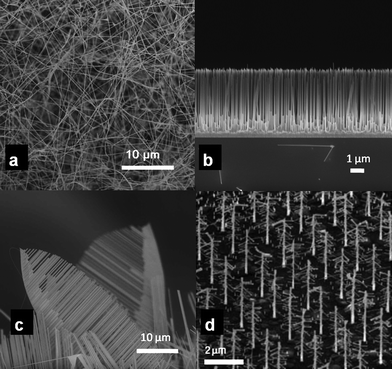 | ||
| Fig. 1 Different morphologies associated with VLS growth: (a) Unaligned SnO2 nanowires (reproduced from ref. 35with permission. Copyright 2010 American Chemical Society); (b) aligned ZnO nanowires grown from a ZnO seed layer; (c) “nanocomb” like hierarchical ZnO nanowire growth; (d) “nanotree” grown through multiple seeding (reproduced from ref. 36 with permission. Copyright 2004 Nature Publishing Group). | ||
Despite the large effort that has been devoted to the catalyst-assisted growth of metal oxide nanowires, the VLS mechanism remains controversial37,38 with continuing debate over the physical state of catalyst particles during VLS growth. ZnO nanowires, for example, grow via a VLS route over a broad range of temperatures. However, a vapor–solid–solid (VSS) mechanism instead of a VLS mechanism was proposed for the growth of ZnO using gold catalyst at low temperatures.39
2.2 Solution-based growth methods
Although the VLS growth technique has proven very successful for the growth of many metal oxides, the reliance of the material to form an eutectic liquid with the catalyst and the high temperatures required for processing that prevent them from being fabricated on plastic and glass substrates are issues which have fuelled the investigation of solution-based growth techniques which have advantages such as high yield, low cost, and easy fabrication. When nanowires are grown using solution-based techniques at low temperatures the growth is driven by chemical decomposition of precursors in the solution rather than physical decomposition. Using these methods, excellent control over the shape and composition, high reproducibility and the formation of hybrid nanostructures have been demonstrated.40,41 The main drawback of solution-grown nanowires is that they show low levels of crystallinity, compared to VLS and similar techniques involving higher temperatures.1One of the most well explored techniques for growing nanowires from solution is hydrothermal synthesis, where the growth of nanowires proceeds with the immersion of a substrate in a heated liquid solution [Fig. 2(a)]. Under typical pressures of 1 atm in an autoclave operating at 100–300 °C, growth is initiated by reactive ions which are thermally degraded from the precursors in the solution. The substrate can have catalysts or nucleation centers of the same material as the nanowires where they can locally lower the surface energy to facilitate nanowire growth. Hydrothermal growth was first introduced to grow single crystals of semiconductors,42 and the process of making ZnO nanostructures by hydrothermal methods was reported in 1990.43 Several different metal oxide nanowires have since been grown by hydrothermal methods, e.g., In2O3,44 Ga2O3,45 and MnO2,46 as well as more complex perovskite structures.47 The multitude of controllable parameters, e.g., substrate preparation, growth temperature, pH etc., makes hydrothermal growth a very powerful tool for complex nanostructures.
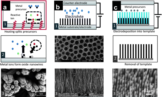 | ||
| Fig. 2 (a) Schematic view of the hydrothermal growth of nanowires: (1) The precursors are heated and reactive (hydroxyl) ions react with metal ions to form metal oxide (2); (3) ZnO nanorods (reproduced from ref. 48 with permission. Copyright 2004 Elsevier). (b) Anodization of a metal electrode generates nanowires (1), TiO2 nanotubes (2) (reproduced from ref. 49 with permission. Copyright 2007 The Royal Society of Chemistry) and (3) ZnO nanowires (reproduced from ref. 50 with permission. Copyright 2010 American Chemical Society). (c) A porous membrane is filled with metal precursors by electrochemical deposition to form aligned nanowires (1); after removal of the membrane (2), free-standing nanowires are formed (3) (reproduced from ref. 51 with permission. Copyright 2004 American Chemical Society). | ||
Apart from hydrothermal growth, another important method is anodization [Fig. 2(b)], in which the substrate is used as an electrode and an applied voltage drives the nanowire growth, which facilitates processing temperatures around room temperature. The nanowires are normally oxides of the electrode metal and are subsequently calcined to improve crystallinity (e.g., ZnO nanowires from Zn,50 Ta2O5 from Ta52 and TiO2 from Ti49).
Methods for generating controlled arrangements of nanowires include template- or patterned-catalyst-assisted growth. In template-based growth, precursor materials are deposited (or solidified), electrochemically or through a sol–gel process or other means, inside a structure comprising pores or manufactured nanochannels [Fig. 2(c)]. The template is thereafter removed, leaving patterns of nanowires. Electrochemical-template-based growth has been reported for ZnO,53 NiO54 and Cu2O;55sol–gel methods for ZrO2,56 TiO2,57 and MnO2.58
2.3 Electrospinning
Electrospinning is a versatile and relatively cost-effective technique for the synthesis of 1D materials of controllable diameter, material composition and porosity.59 Electrospinning was introduced for textile applications in 1934 and to date has been used for generating 1D fibers, wires, tubes, rods with lengths of centimetres and diameters down to 20 nm with materials ranging from polymers to metals, to metal oxides.In the electrospinning process (Fig. 3), the applied electric field overcomes the surface tension of the liquid, forming a continuous jet which upon subsequent solvent evaporation produces nanonets on a collector surface. Solutions containing inorganic metal ions yield high-aspect-ratio inorganic nanonets after appropriate heat treatment. Morphologies such as random, aligned, core–shell, bundles, and mats can be produced by merely changing the collection or injection strategy (Fig. 4). Precise control over the deposition area can be exerted by the incorporation of additional electrodes placed between the spinneret and collector allowing the reduction of the deposition spot size down to 5 mm. Modulating the polymer molecular weight, precursor to polymer ratio as well as the solvent enables the formation of nanoporous structures enabled by phase separation [Fig. 3(g)]. Core–shell nanofibers may also be prepared either by co-spinning or post-spinning dip-coating strategies; and selective thermal treatments yield 1D hollow nanofibers with high aspect ratios.62–64
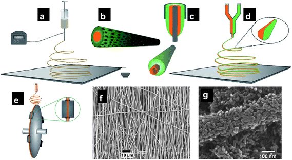 | ||
| Fig. 3 (a) Typical electrospinning setup with a high voltage applied between the spinneret and the grounded collector on which the substrate is placed. Schematic diagrams of (b) a porous nanofiber created through burning-off of polymer precursors or solvent etching, (c) core–shell nanofibers created by using coaxial material sources and (d) bifacial nanofibers. (e) Electrospinning on to a high-speed rotating drum for alignment. (f) Aligned nanofibers (reproduced from ref. 60 with permissio. Copyright 2008 Elsevier). (g) TiO2 nanorods in a nanofiber morphology created using a high-molecular-weight polymer (reproduced from ref. 61 with permission. Copyright 2009 American Chemical Society). | ||
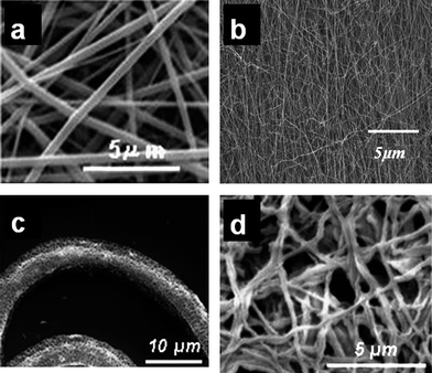 | ||
| Fig. 4 (a) Random TiO2 nanofibers, (b) aligned SnO2 nanofibers, (c) porous ceramic TiO2 fibers obtained after solvothermal treatment and (d) hollow ceramic TiO2 nanofibers obtained using PAN nanofibers as the template. | ||
Blending the dopant into the precursor/polymer solution enables the doping of tin oxide with antimony (Sb) and results in a three-orders of magnitude increase in electrical conductivity of the Sb-doped tin oxide fibers65 or Fe-doped SnO2 nanofibers.66 Electrospun nanofibers may be harvested off the substrate, dispersed in solution, and standard solution processing techniques may be used for device fabrication. Alternatively, as described in the subsequent section, electrospinning may also be used for direct device fabrication by spinning the fibers directly onto the substrate.
3. Nanowire network assembly
A major challenge in utilizing nanowires and nanofibers for practical devices is difficulty in controlling the location and alignment of these nanostructures on the desired substrate. Many strategies for forming network structures with repeatable and controllable strategies have been pursued. These include flow alignment strategies,67,70 Langmuir–Blodgett assembly68,71,72 as well as surface-programmed assembly. These strategies involve the suspension of the nanowires in an appropriate solvent by ultrasonicating the growth substrate before integrating them onto the substrate of interest. The fluidic flow alignment67 process involves directional flow of nanowire suspensions, through microfluidic channels incorporated on the substrate, resulting in the assembly of nanowires in the flow direction [Fig. 5(a)]. The degree of alignment can be controlled by the flow rate with the larger shear forces of higher flow rates reducing the nanowire angular dispersion. The surface coverage increases with flow duration and with functionalisation of the substrate with monolayers that interact favourably with the nanowire surface. Although circuitry fabrication73,74 has been demonstrated on such assembled nanowires, including on plastic substrates,75,76 the low density of the nanowires in such networks makes them unattractive. The Langmuir–Blodgett approach consists of floating a nanowire–surfactant phase on the surface of water [Fig. 5(b)] and the application of a compressive force for densification of the aligned nanowires, which are then transferred onto the substrate.68,71,72 A related assembly technique called the Langmuir–Schaefer technique has also been used to fabricate field-effect transistors.77 Surface-programmed assembly involves forming patterns of self-assembled monolayers (SAMs) on the surface of the receiver substrate through conventional techniques. These patterns induce a difference in the surface properties (charged vs. uncharged, hydrophilic vs. hydrophobic, functionalized vs. unfunctionalized) which would allow the nanowires from the solution to be preferentially adsorbed on to one of the regions. SAM patterns can be created through locally attaching the molecules on the substrate surface (through microcontact printing,78,79 dip-pen lithography80,81) or by selectively removing molecules from a layer through UV light illumination. Surface-programmed self assembly has been employed to assemble V2O5 nanowires69 by patterning SAM molecules to create positively charged and neutral surface regions. V2O5 nanowires which are negatively charged in aqueous solution are attracted to the positively charged regions of the substrate, assembling to form ordered structures [Fig. 5(c)]. Despite significant progress made in the methods described above, the techniques are not well adapted for the fabrication of high-density networks at larger scales. A method gaining attention is direct contact printing, which has demonstrated the potential for easy scalability of network formation.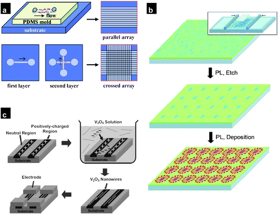 | ||
| Fig. 5 (a) Flow-directed assembly of nanowires (reproduced from ref. 67 with permission. Copyright 2001 The American Association for the Advancement of Science). (b) Process flow for creating Langmuir–Blodgett assemblies for circuitry application (PL refers to photolithography) (reproduced from ref. 68 with permission. Copyright 2004 American Chemical Society). (c) Large-scale surface-programmed assembly of V2O5 nanowires (reproduced from ref. 69 with permission. Copyright 2005 Wiley-VCH). | ||
3.1 Contact printing
The contact printing approach involves the direct transfer of nanowires from the growth substrate to the receiver substrate through shear force. In this process, the growth substrate with vertically grown nanowires is brought into contact with the receiver substrate and gently slid along a particular direction. This technique utilizes shear force to effectively align the nanowires, while van der Waal's forces of attraction and other chemical binding interactions between the substrate and the nanowires allow the nanowires to anchor to the receiver substrate and allow the formation of well-aligned crystalline nanowire networks even on unconventional substrates such as plastic and glass. The density of the nanowire networks is determined by the as-grown nanowire density and can be increased by repeated contact printing. This technique has been demonstrated for the wafer-scale assembly of Si, Ge and CdSe nanowire arrays allowing them to be integrated into transistors and sensors.82–84 This process can also be used in conjunction with transfer printing [Fig. 6(a)] where vertically grown nanowires can be transferred on to another substrate before undergoing contact printing. Patterning of the as-grown nanowires/nanotubes or the transfer layer [e.g. poly(dimethylsiloxane)] allows selective patterning. Another possibility to fabricate nanowire arrays selectively on a substrate is illustrated in Fig. 6(b). Photolithographical patterning of a photoresist on the receiver substrate defines open areas where the transfer of the nanowires from the growth substrate can take place under contact printing. Crossed-nanowire networks can be fabricated by contact printing normal to the previous network. Lift-off of the photoresist completes the process.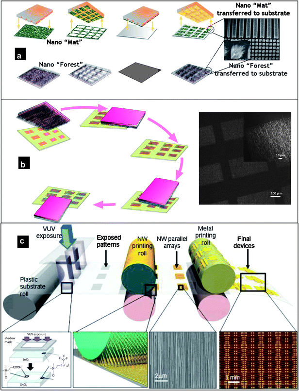 | ||
| Fig. 6 (a) Transfer of nanowire networks (nanomats or nanoforests) through poly(dimethylsiloxane) intermediation (reproduced from ref. 85 with permission. Copyright 2008 Institute of Physics). (b) (Left) schematic illustrating the process flow for selectively patterning substrates with crossed-nanowire networks (reproduced from ref. 86 with permission. Copyright 2010 Springer-Verlag), (right) patterned nanowire networks of SnO2 fabricated through contact printing on to a patterned photoresist followed by lift-off. (c) Schematic of an envisioned roll-to-roll printing set-up. The process involves patterning of a fluorinated monolayer of the receiver substrate to define “sticky” and “non-sticky” regions for contact printing. Following the printing of nanowire active components, devices are fabricated by defining the source/drain and gate electrodes (reproduced from ref. 87 with permission. Copyright 2009 Wiley-VCH). | ||
Roll-to-roll printing [Fig. 6(c)] of nanowires through the contact printing process can also be envisioned by growing the nanowires on a cylindrical substrate.87,88 A differential rolling process has been illustrated with speeds up to 20 mm min−1. Although the printing speeds are far from what is desired for manufacturing, these experiments prove the potential of this technique for printable nanowire electronics.87 An unfortunate consequence of the direct contact printing is the reduction in nanowire lengths due to the shear stresses involved during the transfer. This has consequences for the electrical properties of the nanowire networks, as will be discussed in the subsequent sections.
4. Electronic properties of nanowire networks
In many of the devices fabricated using nanowire networks, the charge transport normally happens across distances less than the average length of the nanowire. This ensures that the electrical properties of the ensemble are determined primarily by the nanowires and the nanowire–metal electrode interface. This is also the case in vertically oriented nanotube array systems utilized for collection of charges in DSSCs and other solar cells. The electrical properties of the vertically oriented nanowire arrays will be discussed in a later section. In systems where the scale is bigger (such as that used in macroelectronics), the charge transport is also determined by the nanowire–nanowire contact.Charge transport through single metal oxide nanowires is strongly dependent on the properties of their surface due to their large area-to-volume ratios as well as their low Debye lengths. This implies that the nanowire's conductivity could completely depend on the chemical processes transpiring on the surface of the nanowire. This has been widely exploited in the fabrication of gas sensors where the addition or depletion of majority carriers due to the adsorption of the gas molecules leads to measurable changes in the nanowire conductivity. The semiconducting nature of metal oxide nanowires such as ZnO, SnO2, In2O3 is normally attributed to oxygen vacancies, metal interstitials or incidental hydrogen.89,90 Temperature-dependent measurements on single ZnO nanowires have revealed that for T >100 K, the conductivity has an activation energy of 30 meV corresponding to the location of the shallow donor levels.91 In SnO2, doubly ionizable oxygen vacancies form levels with energies of 0.030–0.034 eV and 0.14–0.15 eV below the conduction band edge, while hydrogen forms a donor state 0.05 eV below the band edge.92,93 First-principle calculations have also shown the important role played by the tin interstitial and its attraction to the oxygen vacancy leading to the formation of donor states.94
The electrical properties of SnO2 and ZnO individual nanobelts studied in vacuum, in air, and under oxygen, as a function of thermal treatment have suggested that the oxygen adsorption and desorption dynamics depend sensitively on the concentration of surface oxygen vacancies, which, in turn, affect the electron density in the nanobelts.95 Nanobelts annealed in a vacuum were found to have high electron densities and could not be gated; whereas, exposure to low concentrations of oxygen dramatically depletes the electron density in the nanobelts and shifts its threshold potential toward more positive Vg values. Similarly, SnO2 nanowires exposed to high temperatures, inert or reducing atmospheres, behave as highly doped semiconductors or quasi-metals with high conductances that depend weakly on temperature.96 When exposed to oxygen, the nanowires transform to weakly doped semiconductors with high conductance activation energies. The charge-depletion layer induced by surface adsorption completely controls the charge transport in single nanowires, if the diameter of the nanowire is comparable to the depletion layer thickness. A simple strategy to conserve the properties of the nanowire/nanowire network in air is passivation of the surface by deposition of inorganic insulators or polymeric overlayers.35,97–99
Since the semiconducting behavior and the number of charge carriers in metal oxides are dependent on oxygen defects, doping of these oxides has been pursued in order to better control their electrical properties. n-type doping in ZnO was implemented by doping group III (Al, Ga, In) and group IV elements (Sn) into the matrix.100–104 SnO2 nanowires have also been doped through the incorporation of In,105 Sb106,107 and Ta.108 Careful control of the doping density of Sb in SnO2 produced nanowires with high charge carrier mobility (550 cm2 V−1 s−1) at low doping concentrations while high concentrations lead to the formation of a conductor with a resistivity of 5.8 × 10⁻⁴ Ω cm.106 Doping is especially important for the fabrication of air-stable devices, since the increased charge-carrier density leads to a shorter Debye length, making the charge transport in nanowires more stable to adsorbents on the nanowire surface. p-Type doping of these naturally n-type oxides is more difficult to achieve due to self-compensating doping mechanisms by the native defects. P109 and Na110 doping in ZnO nanowires to induce p-type behaviour are recent successes. Another notable example is Fe2O3 which is also n-type due to the presence of oxygen vacancies. However the substitution of Fe3+ by Zn2+ ions at high temperatures (700 °C) results in p-type behaviour.111
Another important determinant of the electrical properties of nanowire networks is the metal–nanowire interface.112 Recent work has shown that the resistivity extracted from I–V measurements of a Pt-SnO2 nanowire device is four orders of magnitude higher than that measured by a non-contact microwave conductivity method.113 This discrepancy was attributed to the presence of an insulating oxidized interfacial layer. Light doping of the nanowires has also been pursued in order to avoid the formation of a Schottky barrier at the metal–nanowire interface.106 Despite having similar work functions (φAl = 4.28 eV and φTi = 4.33 eV), devices fabricated with aluminium contacts displayed higher field-effect mobilities (∼70 cm2 V−1 s−1) than that fabricated with titanium (∼1.3 cm2 V−1 s−1).114 The authors attribute this difference in performance to the poor wetting interaction between the Ti contacts and the ZnO nanowires which could lead to surface states at the metal–nanowire interface, inducing Fermi level pinning and resulting in different Schottky barrier heights.
In addition to the factors described above, charge transport through nanowire networks is also determined by the nanowire–nanowire contacts. As mentioned previously, the absorption of chemical species such as oxygen molecules and OH− radicals cause a change in surface states that affects the width of the conducting channel. Absorbed oxygen molecules may form oxygen ions such as O2− that extract electrons from SnO2, resulting in a depletion of the charge carriers in the nanowire (Fig. 7). In addition, surface-adsorbed H2O and OH groups tend to accumulate electrons to form a positive space charge which further widens the depletion layer.115 The conductance of metal oxide nanowires116,117 can be expressed as G = n0eμπ(D − 2W)2/4l where n0 is the charge carrier density, μ represents the mobility of the charge carriers, D is the diameter of the nanowire, W is the width of the surface charge region and l is the length of the nanowire. The width of this depletion region (W) is given by W = LD(eVs/kT)½ where Vs is the adsorbate-induced band bending while LD is the Debye length. The Debye length in turn is determined as LD = (εε0kT/e2n0)½ where ε is the relative dielectric permittivity of the nanostructure and n0 is the charge-carrier density. The depletion regions in the nanowires act as obstacles that hinder the electron transfer from one nanowire to another, since the current has to pass through the depletion zones of both wires (Fig. 7). Thus, the nanowire junction is the predominant modulator of charge transport in nanowire networks when the diameters of the nanowires exceed the Debye length. The importance of nanowire–nanowire junction on the charge-transport properties of the nanowire network has been exploited in gas sensors,118,119 where it has been observed that sensors fabricated from nanowire ‘mats’ are more sensitive than single nanowire devices. The role of passivation becomes even more critical due to the larger number of nanowire junctions in nanonet devices. Devices which are unpassivated display charge-carrier trapping and large hysteresis windows when tested in air. Drop-casting a layer of poly(styrene) stabilizes the electrical properties of nanowire network transistors.35
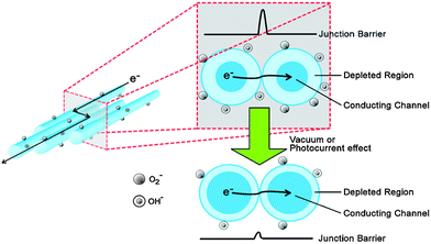 | ||
| Fig. 7 Illustration of the charge transport across nanowire–nanowire junctions. The depletion layer thickness reduces when the sample is in a vacuum or under illumination (reproduced from ref. 35 with permission. Copyright 2010 American Chemical Society). | ||
Fig. 8 shows the application of a contact printing approach to ZnO and SnO2 nanowires to form nanowire network transistors. The ZnO and SnO2 nanowires were grown using standard VLS techniques, before being contact printed on to a silicon nitride substrate. Even though the as-grown SnO2 nanowires on the donor substrate are not ordered [Fig. 1(a)], contact printing yielded highly oriented nanowire networks with nanowire densities estimated at ∼0.3 nanowires per μm2. Area coverage of the nanonets is estimated to be ∼35%. Fast-Fourier transformation (FFT) yields an ellipticity angle of 20° which was observed in the SnO2 nanonets, confirming a very high degree of alignment. Nanowire networks formed from contact printing ZnO nanowires which have a more ordered as-grown structure resulting in a higher level of alignment (ellipticity angle of 10°) indicating that the branched nature of the as-grown SnO2 nanowires limits the level of alignment.35 The scenario for charge transport in nanowire networks is shown in Figure 7. While fabricating transistors from these nanowire networks, the effects of the nanojunctions are visible in both threshold voltage and mobility scaling. This effect is more pronounced in longer channels due to the increasing number of nanojunctions. For SnO2 nanonetwork transistors, the threshold voltages increase from 16 to 23 V with channel lengths increasing from 75 to 175 μm [Fig. 8(e) and (f)]. Similar results on channel length scaling have also been reported for ZnO nanowires.120 In the two transistors illustrated in Fig. 8, it is apparent that the ZnO nanowire network transistor (μ = 0.0145 cm2 V−1 s−1) has poorer charge transport properties than the SnO2 one (μ = 7.5 cm2 V−1 s−1). This could stem from multiple factors. The average length of the ZnO nanowires (6–8 μm) after contact printing is lower than that of SnO2 (10–15 μm), implying a larger number of nanowire–nanowire junctions that act as bottlenecks for the electron transport between the source and drain electrodes. Differences in the nanowire network density may also play a role. The lower density of nanowires in the ZnO network (0.2 nanowires per μm2) reduces the number of charge-transport paths, resulting in lower mobility devices. Differences in the nanowire network density may also play a role. An open question regarding the electron transport in these nanowire networks is the influence of alignment. The importance of alignment in dictating the performance of long-channel transistor (length of channel ≫ length of nanowire) has been previously explored in single-wall carbon nanotube networks.121 In the case of the long-channel transistor, the percolation threshold for a perfectly aligned network approaches infinity. Due to the branched nature of the as-grown SnO2 nanowires, there is a certain level of misalignment built into the system. This bridging of the nanowires could ensure multiple percolation paths and a lower number of “orphan” nanowires.
![(a) A ZnO nanowire network fabricated through contact printing. (b) Transfer characteristics of ZnO nanowire network transistors (L = 75 µm, VDS = 40 V). (c) Output characteristics of a ZnO nanowire network transistor showing good saturation characteristics. (d) A SnO2 nanowire network grown through contact printing. (e) Transfer characteristics of a SnO2 nanowire network transistor for different channel lengths (VDS = 40 V). The inset shows the relevant output characteristics. (f) Channel length scaling effects on mobility and on/off ratios. Insets of (a) and (d) depict the FFT transformations of the nanowire networks indicating their alignment [(d), (e) and (f) are reproduced from ref. 35 with permission. Copyright 2010 American Chemical Society].](/image/article/2010/NR/c0nr00285b/c0nr00285b-f8.gif) | ||
| Fig. 8 (a) A ZnO nanowire network fabricated through contact printing. (b) Transfer characteristics of ZnO nanowire network transistors (L = 75 µm, VDS = 40 V). (c) Output characteristics of a ZnO nanowire network transistor showing good saturation characteristics. (d) A SnO2 nanowire network grown through contact printing. (e) Transfer characteristics of a SnO2 nanowire network transistor for different channel lengths (VDS = 40 V). The inset shows the relevant output characteristics. (f) Channel length scaling effects on mobility and on/off ratios. Insets of (a) and (d) depict the FFT transformations of the nanowire networks indicating their alignment [(d), (e) and (f) are reproduced from ref. 35 with permission. Copyright 2010 American Chemical Society]. | ||
The use of nanowire networks in conjunction with organic semiconductors is also a feasible approach to fabricating large-scale printed devices with unique properties. The combination of a ZnO nanowire network and an n-type semiconductor [6,6]-phenyl-C61-butyric acid methyl ester (PCBM) yielded devices with good transistor characteristics. Fig. 9(a) displays the electrical characteristics of one such transistor. The saturation field-effect mobility of pristine PCBM is 0.0334 cm2 V−1 s−1, and the on/off current ratio is 9 × 10⁵, while for a ZnO-PCBM thin-film transistor device, the field-effect mobility is increased to 0.561 cm2 V−1 s−1, representing an improvement of more than 17 times over the pristine PCBM thin-film transistor device. The incorporation of ZnO nanowires produces a higher on-current, higher mobility, steeper subthreshold slope, and a reduced threshold voltage (closer to zero). The increase in the field-effect mobility is attributed to the superior semiconducting properties of ZnO. The nanowires could be viewed as conducting bridges which serve to enhance electron transport between crystals in the PCBM film while also contributing an increased number of charge carriers in the transport channel.122 The combination of a p-type organic semiconductor and an n-type metal oxide nanowire network allows the ambipolar operation of the transistor. Fig. 9(b) displays the electrical characteristics of such a transistor. Drop-casting a layer of poly(3-hexylthiophene) (P3HT) over a SnO2 transistor allows the operation of the transistor in two regimes. In the testing configuration displayed in Fig. 9(b) inset, the drain and the gate terminals of the transistor are grounded and only the source voltage is modulated. The application of a positive source voltage induces a negative gate, drain bias and thus accumulates holes in the transistor channel. Conversely, the application of a negative source voltage induces electrons in the transistor channel. Since the mobility of organic semiconductors are generally lower than that of the SnO2 nanonet devices, the current levels in the two operating regimes are asymmetric. Further optimization of this category of metal oxide–organic semiconductor nanocomposite transistors would involve improving the morphology of the organic semiconducting layer to improve performance, as well as the deposition of an interlayer between the n-type semiconductor and p-type semiconductor to prevent recombination of the charge carriers.
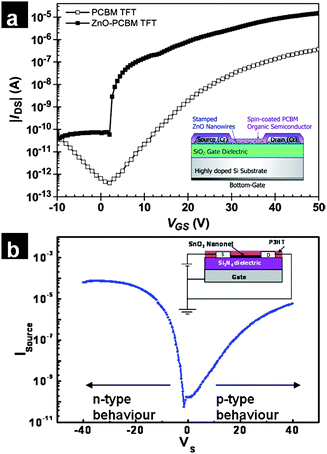 | ||
| Fig. 9 (a) Transfer characteristics of ZnO nanowire network–PCBM composite transistors (reproduced from ref. 122with permission. Copyright 2008 IEEE). (b) Transfer characteristics of an SnO2 nanowire network–P3HT composite layer displaying ambipolar characteristics. | ||
High-performance transistors fabricated from oxide nanowire networks have demonstrated the potential for employing this material set in macroelectronics (large-area electronics). The influence of factors such as nanowire doping on the scaling effects of these networks as well as the tolerance of the electrical properties to nanowire misalignment need to be studied in detail before true wafer-scale integration of these networks is possible.
5. Photocurrent generation in nanowires
The optical properties of oxide nanowires have been studied extensively in recent years and their potential explored in various fields including light detection, optical switches, optoelectronic components, and in solar energy harvesting.123–126 The 1D geometry and the nanometric size of nanowires endow them with unique optical properties which are different (or in some cases absent) from bulk materials. Polarization-sensitive photocurrent arising from the 1D geometry of the nanowires is a prototypical example.127 The photoresponse of nanowires is usually evaluated by monitoring the changes in electrical properties of nanowires upon irradiation of light. Typically the experiments are performed on individual or an ensemble of nanowires, which are contacted with metal electrodes in a resistor or field-effect transistor configuration. Studies on the photoresponse of individual oxide 1D nanostructures have revealed the effects of size,128 geometry,129 and the key role of the metal contact.129,130 The predominant role of surface states and charge-trapping surface adsorbents on the photoresponse of oxide nanowires has been reported by various researchers.131–133 The dependence of incident light wavelength, intensity, and pulse duration on the electrical conductivity of nanowires provides significant insight into its electronic structure, defect and surface states, carrier lifetime and transport properties.Although the small size of the nanowires is expected to limit the light absorption efficiency of isolated nanowires, early work on the photoresponse of individual ZnO nanowires demonstrated their ultra-high UV sensitivity.134 A 4–6 orders of magnitude enhancement in conductivity of ZnO nanowires upon UV irradiation was observed. The UV response of ZnO nanowires has been studied by various researchers to understand the underlying mechanism of such large conductivity variations.132,133,135 Measurements in a controlled atmosphere have revealed desorption of charge-trapping surface chemisorbed ions, upon UV irradiation as the key mechanism for the increase in electrical conductivity. As mentioned previously, the adsorption of O2− ions onto the surface of the ZnO nanowires, creates a depletion region on the surface of the nanowire. The resultant charge inhomogeneity induced band bending drives photogenerated holes towards the surface and discharges the oxygen ions facilitating their desorption as oxygen molecules. Thus the electron–hole recombination rate is largely suppressed and the photogenerated free electrons increase the conductivity of the nanowire.130 The UV photoresponse of various wide-bandgap metal oxide 1D structures, including SnO2 (Eg ∼3.6 eV),128 Ga2O3 (Egca. 4.4–4.8 eV)136 and W18O49137 nanowires have also been studied by various researchers. By introducing charge-hopping states via surface coating with polymers the UV sensitivity of oxides nanowires can be further enhanced.138,139Fig. 10(a) and (b) illustrate the effect of different polymer coating on the UV photoresponse of ZnO nanobelts.138 Poly(styrenesulfonate) (PSS) coated ZnO nanobelts showed better UV sensitivity as compared with poly(styrene-co-maleic acid) (PS-co-MAc) coated and bare ZnO nanobelts [Fig. 10(a)]. The enhanced photoresponse of PSS-coated nanobelts was attributed to the high light absorption efficiency and favorable energy levels of PSS, which facilitate the carrier generation in PSS and transfer to ZnO nanobelts [Fig. 10(b)]. In addition, hybrid oxide 1D structures fabricated by surface coating/decoration with metal/inorganic nanoparticles were found to exhibit improved photosensing functionalities. For example, by attaching Au nanoparticles to a SnO2 nanowire surface the UV sensitivity was found to be enhanced significantly.140 The observed high optical gain was explained on the basis of localized Schottky barrier formation near the vicinity of the Au nanoparticles. The presence of charge-separating Schottky barriers prolongs the photogenerated carrier lifetime and therefore improves the photoconductivity. Similarly, studies on ZnO nanowires decorated with ZnO nanoparticles,141 CdTe quantum dots142 and ZnO–ZnS hybrid nanowires143 demonstrated the effect of heterojunctions in enhancing the photocurrent and sensitivity of nanowire photodetectors.
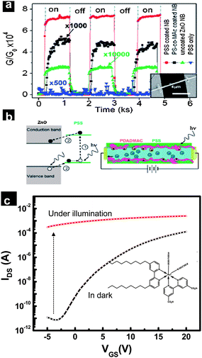 | ||
| Fig. 10 (a) UV response of ZnO nanobelts coated with different polymers. (b) Schematic illustration of carrier photogeneration and transport processes in PSS-coated ZnO nanobelts (reproduced from ref. 138 with permission. Copyright 2007 American Chemical Society). (c) Photocurrent effect on transfer characteristics of SnO2 nanowire network transistors sensitized by Z907 dye. The structure of the dye is provided in the inset. | ||
In addition to single-nanowire studies, the photoresponse of a percolated network of oxide nanowires including ZnO, Zn2GeO4 (Eg ∼4.68 eV) and SnO2 nanowires have also been reported.144,145 The high resistance, arising from the large number of nanowire–nanowire contacts, reduces the dark current in nanowire networks and high photosensitivity can thus be achieved. In nanowire network photodetectors, there are two mechanisms at play, the oxygen desorption mechanism as well as nanowire–nanowire junction barrier modification upon UV irradiation (Fig. 7).144 Many of the metal oxides that could be easily fabricated in 1D structures using recently developed bottom-up approaches have wide bandgaps resulting in low sensitivity towards visible light. Alternatively, using nanowires whose bandgap energy lies in the visible range (e.g. Cu2O, CdO) results in photosensors with high sensitivity towards the visible range due to direct band-to-band excitation.146,147 In addition, wide-bandgap metal oxide nanowires can be made sensitive to visible/infrared irradiation by doping. Cu- and Al-doped ZnO nanowires exhibited improved photoconductivity in the visible and infrared ranges due to defect level excitation.148,149Fig. 10(c) illustrates the photocurrent properties of a SnO2 nanonet transistor decorated with a RuLL′(NCS)2·2H2O (L = 2,2′-bipyridyl-4,4′-dicarboxylic acid; L′ = 4,4′-dinonyl-2,2′-bipyridine) dye (also called Z907). The carboxylic groups in the Z907 dye allow it to adsorb easily on the oxide nanowire surface. As seen from the transfer characteristics of the transistor, the current level under photoillumination increases by about 7 orders of magnitude indicating efficient charge injection from the dye into the metal oxide nanowires.
Despite the large efforts made in recent years to understand the mechanism of various processes occurring during the nanowire–photon interaction, several unanswered questions persist. The mechanism underlying the photogeneration, transport and collection at the electrodes of charge carriers are complicated due to multiple contributing factors. Recently developed localized photocurrent measurement techniques using near-field optical microscopy or focused laser beams were found to be an efficient tool to locally probe and characterize silicon/germanium nanowires and carbon-nanotube-based nanodevices.150–152 Local photocurrent measurements were successfully employed to asses the nature of nanotube–metal contacts, and to determine carrier diffusion length in single-nanowire solar cells.152 Similar studies on metal oxide nanowires and hybrid nanowires based on metal oxides would further strengthen our understanding of the photogeneration and transport mechanism of charge carriers.
6. Oxide nanowire networks in solar cells
The optoelectronic properties of metal oxide nanowires and their hybrid structures hold potential for applications in DSSCs.153,154 In these solar cells,155–157 a thick film comprising dye adsorbed metal oxide nanoparticles acts as a photoanode, while platinum-coated fluorinated tin oxide (FTO) glass acts as a cathode with a redox electrolyte inserted between the electrodes. The dye molecule is the absorber, the nanoparticles the electron transporters, with the electrolyte and the anode being responsible for charge transport and dye regeneration. Charge transport through interconnected nanoparticles and the particle surface area related to dye adsorption and photogeneration, are critical elements in determining the power conversion efficiency (η) of the DSSC. The large clusters of dye molecules that cover the surface of the metal oxide also decrease the number of surface recombination centers, leading to an increase in η.158 In conventional DSSCs, the metal oxide layer is about 10 μm thick and consists of TiO2 nanoparticles which provides a large surface area for the grafting of dye molecules and hence photon harvesting. However the photogenerated electrons can also be trapped at surface states or defect states, which slow down the electron transport.159–162 It has been reported that for a nanoparticle film with 50% porosity, the average number of nanoparticles visited by the electron is about 106.163The use of nanowires allows the formation of a direct conduction path for the photogenerated carriers to the electrode in contrast to the 0D structure based solar cells where the conduction is limited by several charge-hopping events between individual particles. This ensures that the mobility of the electrons in the nanowire-based solar cells is much higher than the nanoparticle-based solar cells. Other significant differences include the diameter of the nanowires, which allows for the formation of a depletion region at the surface which acts as a potential barrier that drives the exciton splitting at the dye–nanowire interface. The band bending also sweeps the electrons away from the surface of the nanowire, reducing the chances of recombination. Improved kinetics154of charge transfer at the dye–semiconductor interface for nanowires was observed through transient absorption spectroscopy with bi-exponential kinetics (time constants: 250 ps, 3 ps), whereas the particle response was tri-exponential and significantly slower (time constants: <250 fs, 20 ps, 200 ps). The disadvantage of such nanowire-based solar cells is their low surface area which limits the total amount of adsorbed dye. TiO2-based hollow nanotube arrays provide larger surface areas while maintaining the advantages of the 1D architecture. These nanotube arrays have been mainly fabricated by anodization of Ti foil (η = 6.9%)164 or on thick Ti films on FTO substrates.165,166 An alternative approach involves the transfer of the nanotube arrays from Ti foils on to transparent electrodes (η = 9.1%).167–169
6.1 Electrospun nanowire networks for DSSCs
As described in the previous section, electrospun fibers may be harvested and then screen printed,170 sprayed171 or directly electrospun on to the anode172en route to solar cell fabrication. Oxide nanofibers with large surface areas enhance dye adsorption and thereby improve the power conversion efficiency. High-surface-area TiO2 nanofibers were successfully prepared by electrospinning from a blend of titanium precursors (titanium propoxides/butoxides) and high-molecular-weight polymers e.g. poly(vinyl acetate) (PVAc), poly(vinyl pyrrolidone) (PVP) and poly(ethylene oxide) (PEO).170,173 By selecting the appropriate molecular weight of polymer and concentration ratio of polymer to the metal oxide precursors, size-controlled nanorod morphologies within nanofibrous structures can be obtained. Kim and coworkers61 used high-molecular-weight PVAc (106) to induce phase separation, resulting in the formation of TiO2 nanorods of size 15–30 nm within 60 nm diameter sintered nanofibers with a specific surface area of 123 m2 g−1 m−1 (pore volume: 1.28 cm3 g−1 m−1) as pictured in Fig. 3(g). The resultant dye loading (8.59 × 10⁻⁸ mol mg−1) was 2.5 times greater than that from TiO2 nanoparticles (3.44 × 10⁻⁸mol mg−1) and yielded efficiencies of 9–11% similar to the highest efficiencies obtained using TiO2 nanoparticles.61 This difference in the dye loading between the nanoparticle-based cell and the nanorod morphology is seen in the incident-photon-to-charge-carrier efficiency (IPCE) spectra of the solar cells [Fig. 11(a)]. Electrospun nanofibers facilitate longer electron lifetimes,174 and improve effective electron diffusion coefficients (Deff), thus improving carrier collection and device efficiencies.170 Other materials used to make nanowire-based solar cells include ZnO (PEO/poly(vinyl alcohol) and zinc acetate),175,176 SnO2 (PEO/PVP and SnCl4/SnCl2·2H2O/tin(IV) ethylhexanoate).66,177,178 Charge transport in the oxide nanofibers may also be improved by incorporating carbon nanotubes during electrospinning.179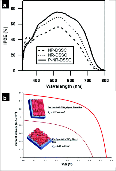 | ||
| Fig. 11 (a) IPCE spectra of nanoparticle (‘NP-DSSC’), nanorod morphology (‘NR-DSSC’) and TiCl4-treated nanorod morphology (‘P-NR-DSSC’) based dye-sensitized solar cells (reproduced from ref. 61 with permission. Copyright 2009 American Chemical Society). (b) J–V profiles of random and aligned ceramic TiO2 nanofiberous film based dye-sensitized solar cells. | ||
The systems discussed above have been limited to random nanowire networks. Electrospinning using a high-speed rotating disc or drum as the collector enables the production of nanofibers in uniaxial as well as cross-aligned arrays.180 The aligned nanofiber architecture significantly enhances the packing density (oxide nanowires per unit area), increasing the quantity of absorbed dye, and thus improving the cell efficiency. Initial results showed [Fig. 11(b)] that the introduction of an aligned architecture (TiO2 nanofibers, 78–100 nm diameter) into a DSSC increased the open-circuit voltage (Voc) by 20% and the short-circuit current (Jsc) by ∼70%, thus confirming that aligned 1D nanofibers could improve the electron transport and also the carrier collection rate in DSSCs.
7. Future outlook and concluding remarks
Oxide nanowire networks thus form a very attractive material set with properties that can find applications in nanoelectronics and photovoltaic energy harvesting. The properties of these networks can be tuned by changing the geometrical dimensions (length, diameter) of the nanowires, the nanowire density as well as the dopant concentration. In addition, the nanowire networks provide advantages in flexibility and fault tolerance which makes them amenable for applications in flexible electronics. Transistors fabricated at length scales bigger than the nanowire length show impressive performance, indicating that the nanowire–nanowire junction, although important, is not a limiting factor. The use of appropriate passivation strategies as well as doping to increase charge carriers will ensure that these networks are stable in ambient conditions.Oxide nanowires in solar cells (esp. DSSCs) have proven to be advantageous with their 1D morphology ensuring a good transport path for the photogenerated carriers to the electrode. Band bending at the oxide–dye interface allows more efficient splitting of the excitons. The low surface area limitation for these 1D nanostructures in solar cells can be addressed through development of hyperbranched nanowires, which provide additional area for photoharvesting as well as light-scattering effects.181 Other strategies to boost photovoltaic efficiencies could include core–shell nanowire structures where the electronic structure of the shell material favours exciton splitting while the core possesses superior charge transport properties.
In order for oxide nanowire networks to become widely employed in macroelectronics and other applications, the processes of nanowire growth and network formation have to be scaled up. Solution-based methods for growing large quantities of highly crystalline nanowires have to be explored. Challenges in network formation include accurate placement with respect to underlying layers as well as ensuring that the deposited nanowires do not have their lengths drastically reduced during printing. To enable integration of the nanowire networks, top-gate architectures for the nanowire network transistors have to be demonstrated, indicating that planarization strategies for the networks have to be developed. The technological utility of these networks has to be also demonstrated by integration on to glass and plastic substrates. This would entail the development of protocols to transfer deposited nanowire networks through lamination.
In addition to the areas discussed in this paper, there are many fields in which oxide nanowires could play a major role. One of them is in the development of transparent conducting films. Networks of large-bandgap metal oxide nanowires which are doped to increase conductivity could act as electrodes with high surface areas, allowing efficient charge collection in photovoltaics. Oxide nanowire networks are also envisioned to play an increasingly important role in other areas associated with energy harvesting and storage. The electrochemical storage properties of nanowire networks have been proven to be superior to that composed of nanoparticle composites. The high surface area of the 1D structure coupled with the pseudocapacitance properties of metal oxides increases the energy density of the electrochemical capacitors. Morphologies such as conducting core–oxide shell need to be pursued in order to ensure low electrode resistances.182 Hollow nanotubes are also expected to play an important role in lithium-ion batteries, due to their increased conductivity values and the alleviation of stress caused by lithium intercalation.183,184 Direct production of hydrogen from solar energy is another application that metal oxide networks are ideally placed to target. The poor transport properties plaguing many photosensitive oxides can be improved through the formation of high-quality nanowire networks.185
References
- Y. Xia, P. Yang, Y. Sun, Y. Wu, B. Mayers, B. Gates, Y. Yin, F. Kim and H. Yan, Adv. Mater., 2003, 15, 353–389 CrossRef CAS.
- M. M. C. Cheng, G. Cuda, Y. L. Bunimovich, M. Gaspari, J. R. Heath, H. D. Hill, C. A. Mirkin, A. J. Nijdam, R. Terracciano, T. Thundat and M. Ferrari, Curr. Opin. Chem. Biol., 2006, 10, 11–19 CrossRef CAS.
- M. Law, J. Goldberger and P. D. Yang, Annu. Rev. Mater. Res., 2004, 34, 83–122 CrossRef CAS.
- Y. Li, F. Qian, J. Xiang and C. M. Lieber, Mater. Today, 2006, 9, 18–27 CrossRef CAS.
- W. Lu and C. M. Lieber, Nat. Mater., 2007, 6, 841–850 CrossRef CAS.
- P. J. Pauzauskie and P. Yang, Mater. Today, 2006, 9, 36–45 CrossRef CAS.
- H. J. Dai, Surf. Sci., 2002, 500, 218–241 CrossRef CAS.
- T. Dürkop, B. M. Kim and M. S. Fuhrer, J. Phys.: Condens. Matter, 2004, 16, R553–R580 CrossRef.
- Q. Cao and J. A. Rogers, Adv. Mater., 2009, 21, 29–53 CrossRef CAS.
- W. Lu and C. M. Lieber, J. Phys. D: Appl. Phys., 2006, 39, R387–R406 CrossRef CAS.
- V. Schmidt, J. V. Wittemann, S. Senz and U. Gösele, Adv. Mater., 2009, 21, 2681–2702 CrossRef CAS.
- Z. L. Wang, J. Nanosci. Nanotechnol., 2008, 8, 27–55 CrossRef CAS.
- Y. W. Heo, D. P. Norton, L. C. Tien, Y. Kwon, B. S. Kang, F. Ren, S. J. Pearton and J. R. LaRoche, Mater. Sci. Eng., R, 2004, 47, 1–47 CrossRef.
- C. D. Dimitrakopoulos and P. R. L. Malenfant, Adv. Mater., 2002, 14, 99–117 CrossRef CAS.
- N. Mathews, Y. M. Lam, S. G. Mhaisalkar and A. C. Grimsdale, Int. J. Mater. Res., 2010, 101, 236–250 Search PubMed.
- A. C. Arias, J. D. MacKenzie, I. McCulloch, J. Rivnay and A. Salleo, Chem. Rev., 2010, 110, 3–24 CrossRef CAS.
- S. Campidelli, M. Meneghetti and M. Prato, Small, 2007, 3, 1672–1676 CrossRef CAS.
- Q. Cao, H. S. Kim, N. Pimparkar, J. P. Kulkarni, C. Wang, M. Shim, K. Roy, M. A. Alam and J. A. Rogers, Nature, 2008, 454, 495–500 CrossRef CAS.
- V. Schmidt, J. V. Wittemann and U. Gösele, Chem. Rev., 2010, 110, 361–388 CrossRef CAS.
- K. Heo, E. Cho, J. E. Yang, M. H. Kim, M. Lee, B. Y. Lee, S. G. Kwon, M. S. Lee, M. H. Jo, H. J. Choi, T. Hyeon and S. Hong, Nano Lett., 2008, 8, 4523–4527 CrossRef CAS.
- N. Wang, Y. Cai and R. Q. Zhang, Mater. Sci. Eng., R, 2008, 60, 1–51 CrossRef.
- R. S. Wagner and W. C. Ellis, Appl. Phys. Lett., 1964, 4, 89–90 CAS.
- R. S. Wagner and R. G. Treuting, J. Appl. Phys., 1961, 32, 2490–2491 CrossRef CAS.
- Y. Liu, Q. Li and S. Fan, Chem. Phys. Lett., 2003, 375, 632–635 CrossRef CAS.
- Q. Wan, M. Wei, D. Zhi, J. L. MacManus-Driscoll and M. G. Blamire, Adv. Mater., 2006, 18, 234–238 CrossRef CAS.
- G. D. Yuan, W. J. Zhang, J. S. Jie, X. Fan, J. A. Zapien, Y. H. Leung, L. B. Luo, P. F. Wang, C. S. Lee and S. T. Lee, Nano Lett., 2008, 8, 2591–2597 CrossRef CAS.
- K. C. Kam, F. L. Deepak, A. K. Cheetham and C. N. R. Rao, Chem. Phys. Lett., 2004, 397, 329–334 CrossRef CAS.
- C. N. R. Rao, G. Gundiah, F. L. Deepak, A. Govindaraj and A. K. Cheetham, J. Mater. Chem., 2004, 14, 440–450 RSC.
- J. Zhang, F. Jiang, Y. Yang and J. Li, J. Phys. Chem. B, 2005, 109, 13143–13147 CrossRef CAS.
- K. Nagashima, T. Yanagida, H. Tanaka, S. Seki, A. Saeki, S. Tagawa and T. Kawai, J. Am. Chem. Soc., 2008, 130, 5378–5382 CrossRef CAS.
- P. Nguyen, H. T. Ng and M. Meyyappan, Adv. Mater., 2005, 17, 1773–1777 CrossRef CAS.
- T. Yanagida, K. Nagashima, H. Tanaka and T. Kawai, J. Appl. Phys., 2008, 104, 016101–016103 CrossRef.
- H. Li, Y. Huang, Y. Zhang, J. Qi, X. Yan, Q. Zhang and J. Wang, Cryst. Growth Des., 2009, 9, 1863–1868 CrossRef CAS.
- D.-W. Kim, I.-S. Hwang, S. J. Kwon, H.-Y. Kang, K.-S. Park, Y.-J. Choi, K.-J. Choi and J.-G. Park, Nano Lett., 2007, 7, 3041–3045 CrossRef CAS.
- C. Sun, N. Mathews, M. Zheng, C. H. Sow, L. H. Wong and S. G. Mhaisalkar, J. Phys. Chem. C, 2010, 114, 1331–1336 CrossRef CAS.
- K. A. Dick, K. Deppert, M. W. Larsson, T. Mårtensson, W. Seifert, L. R. Wallenberg and L. Samuelson, Nat. Mater., 2004, 3, 380–384 CrossRef CAS.
- K. W. Kolasinski, Curr. Opin. Solid State Mater. Sci., 2006, 10, 182–191 CrossRef CAS.
- A. Vomiero, M. Ferroni, E. Comini, G. Faglia and G. Sberveglieri, Cryst. Growth Des., 2010, 10, 140–145 CrossRef CAS.
- L. C. Campos, M. Tonezzer, A. S. Ferlauto, V. Grillo, R. Magalhães-Paniago, S. Oliveira, L. O. Ladeira and R. G. Lacerda, Adv. Mater., 2008, 20, 1499–1504 CrossRef CAS.
- C. Nasr, S. Hotchandani, W. Y. Kim, R. H. Schmehl and P. V. Kamat, J. Phys. Chem. B, 1997, 101, 7480–7487 CrossRef CAS.
- S. S. Davis, Trends Biotechnol., 1997, 15, 217–224 CrossRef CAS.
- V. A. Kuznetsov, I. P. Kuzmina and I. M. Sylvestrova, Bull. Mater. Sci., 1984, 6, 177–192 Search PubMed.
- M. A. Vergés, A. Mifsud and C. J. Serna, J. Chem. Soc., Faraday Trans., 1990, 86, 959 RSC.
- L. Dai, X. L. Chen, J. K. Jian, M. He, T. Zhou and B. Q. Hu, Appl. Phys. A: Mater. Sci. Process., 2002, 75, 687–689 CrossRef CAS.
- J. Zhang, Z. G. Liu, C. K. Lin and J. Lin, J. Cryst. Growth, 2005, 280, 99–106 CrossRef CAS.
- D. S. Zheng, S. X. Sun and W. L. Fan, J. Phys. Chem. B, 2005, 109, 16439 CrossRef CAS.
- D. L. Zhu, H. Zhu and Y. H. Zhang, J. Cryst. Growth, 2003, 249, 172 CrossRef CAS.
- Z. Wang, X.-f. Qian, J. Yin and Z.-k. Zhu, J. Solid State Chem., 2004, 177, 2144–2149 CrossRef CAS.
- C. A. Grimes, J. Mater. Chem., 2007, 17, 1451 RSC.
- Z. Hu, Q. Chen, Z. Li, Y. Yu and L.-M. Peng, J. Phys. Chem. C, 2010, 114, 881–889 CrossRef CAS.
- Y. Liang, C. Zhen, D. Zou and D. Xu, J. Am. Chem. Soc., 2004, 126, 16338–16339 CrossRef CAS.
- N. K. Allam, X. J. Feng and C. A. Grimes, Chem. Mater., 2008, 20, 6477–6481 CrossRef CAS.
- M. J. Zheng, L. D. Zhang, G. H. Li and W. Z. Shen, Chem. Phys. Lett., 2002, 363, 123 CrossRef CAS.
- T. S. Mintz, Y. V. Bhargava, S. A. Thorne, R. Chopdekar, V. Radmilovic, Y. Suzuki and T. M. Devine, Electrochem. Solid-State Lett., 2005, 8, D26 CrossRef CAS.
- X. M. Liu and Y. C. Zhou, Appl. Phys. A: Mater. Sci. Process., 2005, 689, 685–689 CrossRef.
- H. Xu, D. H. Qin, Z. Yang and H. L. Li, Chem. Phys., 2003, 80, 524 CAS.
- M. Zhang, Y. Bando and K. Wada, J. Mater. Sci. Lett., 2001, 20, 167–170 CrossRef CAS.
- X. Y. Wang, W. G. Huang, P. J. Sebastian and S. Gamboa, J. Power Sources, 2005, 140, 211–215 CrossRef CAS.
- D. Li and Y. Xia, Adv. Mater., 2004, 16, 1151–1170 CrossRef CAS.
- W. A. Yee, A. C. Nguyen, P. S. Lee, M. Kotaki, Y. Liu, B. T. Tan, S. Mhaisalkar and X. Lu, Polymer, 2008, 49, 4196–4203 CrossRef CAS.
- B.-H. Lee, M.-Y. Song, S.-Y. Jang, S.-M. Jo, S.-Y. Kwak and D.-Y. Kim, J. Phys. Chem. C, 2009, 113, 21453–21457 CrossRef CAS.
- H. Wu, D. Lin and W. Pan, Appl. Phys. Lett., 2006, 89, 133125 CrossRef.
- V. Thavasi, G. Singh and S. Ramakrishna, Energy Environ. Sci., 2008, 1, 205–221 RSC.
- X. Lu, C. Wang and Y. Wei, Small, 2009, 5, 2349–2370 CrossRef CAS.
- N. León-Brito, A. Melendez, I. Ramos, N. J. Pinto and J. J. Santiago-Aviles, J. Phys. Conf. Ser., 2007, 61, 683–687 CrossRef CAS.
- Z. Wang and L. Liu, Mater. Lett., 2009, 63, 917–919 CrossRef CAS.
- Y. Huang, X. Duan, Q. Wei and C. M. Lieber, Science, 2001, 291, 630–633 CrossRef CAS.
- S. Jin, D. Whang, M. C. McAlpine, R. S. Friedman, Y. Wu and C. M. Lieber, Nano Lett., 2004, 4, 915–919 CrossRef CAS.
- S. Myung, M. Lee, G. T. Kim, J. S. Ha and S. Hong, Adv. Mater., 2005, 17, 2361–2364 CrossRef CAS.
- X. Duan, C. Niu, V. Sahi, J. Chen, J. W. Parce, S. Empedocles and J. L. Goldman, Nature, 2003, 425, 274–278 CrossRef CAS.
- A. Tao, F. Kim, C. Hess, J. Goldberger, R. He, Y. Sun, Y. Xia and P. Yang, Nano Lett., 2003, 3, 1229–1233 CrossRef CAS.
- S. Acharya, A. B. Panda, N. Belman, S. Efrima and Y. Golan, Adv. Mater., 2006, 18, 210–213 CrossRef CAS.
- Y. Huang, X. Duan, Y. Cui, L. J. Lauhon, K. H. Kim and C. M. Lieber, Science, 2001, 294, 1313–1317 CrossRef CAS.
- Z. Zhong, D. Wang, Y. Cui, M. W. Bockrath and C. H. Lieber, Science, 2003, 302, 1377–1379 CrossRef CAS.
- M. C. McAlpine, R. S. Friedman, S. Jin, K.-h. Lin, W. U. Wang and C. M. Lieber, Nano Lett., 2003, 3, 1531–1535 CrossRef CAS.
- M. C. McAlpine, R. S. Friedman and C. M. Lieber, Nano Lett., 2003, 3, 443–445 CrossRef CAS.
- D. Whang, S. Jin, Y. Wu and C. M. Lieber, Nano Lett., 2003, 3, 1255–1259 CrossRef CAS.
- S. G. Rao, L. Huang, W. Setyawan and S. Hong, Nature, 2003, 425, 36–37 CrossRef CAS.
- S. Alom Ruiz and C. S. Chen, Soft Matter, 2007, 3, 168–177 RSC.
- R. D. Piner, J. Zhu, F. Xu, S. Hong and C. A. Mirkin, Science, 1999, 283, 661–663 CrossRef CAS.
- Y. Wang, D. Maspoch, S. Zou, G. C. Schatz, R. E. Smalley and C. A. Mirkin, Proc. Natl. Acad. Sci. U. S. A., 2006, 103, 2026–2031 CrossRef CAS.
- Z. Fan, J. C. Ho, Z. A. Jacobson, R. Yerushalmi, R. L. Alley, H. Razavi and A. Javey, Nano Lett., 2008, 8, 20–25 CrossRef CAS.
- A. Javey, S. Nam, R. S. Friedman, H. Yan and C. M. Lieber, Nano Lett., 2007, 7, 773–777 CrossRef CAS.
- Z. Fan, J. C. Ho, Z. A. Jacobson, H. Razavi and A. Javey, Proc. Natl. Acad. Sci. U. S. A., 2008, 105, 11066–11070 CrossRef CAS.
- Y. Zhu, X. Lim, M. C. Sim, C. T. Lim and C. H. Sow, Nanotechnology, 2008, 19, 325304 CrossRef.
- J. N. Tey, I. P. M. Wijaya, J. Wei, I. Rodriguez and S. G. Mhaisalkar, Microfluid. Nanofluid., 2010 DOI:10.1007/s10404-010-0640-1.
- Z. Fan, J. C. Ho, T. Takahashi, R. Yerushalmi, K. Takei, A. C. Ford, Y. L. Chueh and A. Javey, Adv. Mater., 2009, 21, 3730–3743 CrossRef CAS.
- R. Yerushalmi, Z. A. Jacobson, J. C. Ho, Z. Fan and A. Javey, Appl. Phys. Lett., 2007, 91, 203104 CrossRef.
- A. K. Singh, A. Janotti, M. Scheffler and C. G. Van De Walle, Phys. Rev. Lett., 2008, 101, 055502 CrossRef.
- P. D. C. King, R. L. Lichti, Y. G. Celebi, J. M. Gil, R. C. Vilão, H. V. Alberto, J. Piroto Duarte, D. J. Payne, R. G. Egdell, I. McKenzie, C. F. McConville, S. F. J. Cox and T. D. Veal, Phys. Rev. B: Condens. Matter Mater. Phys., 2009, 80, 081201 CrossRef.
- P. C. Chang and J. G. Lu, Appl. Phys. Lett., 2008, 92, 212113 CrossRef.
- C. G. Fonstad and R. H. Rediker, J. Appl. Phys., 1971, 42, 2911–2918 CrossRef.
- S. Samson and C. G. Fonstad, J. Appl. Phys., 1973, 44, 4618–4621 CrossRef CAS.
- Ç. Kılıç and A. Zunger, Phys. Rev. Lett., 2002, 88, 095501–955014 CrossRef.
- M. S. Arnold, P. Avouris, Z. W. Pan and Z. L. Wang, J. Phys. Chem. B, 2003, 107, 659–663 CrossRef CAS.
- A. Kolmakov, Y. Zhang, G. Cheng and M. Moskovits, Adv. Mater., 2003, 15, 997–1000 CrossRef CAS.
- W. K. Hong, B. J. Kim, T. W. Kim, G. Jo, S. Song, S. S. Kwon, A. Yoon, E. A. Stach and T. Lee, Colloids Surf., A, 2008, 313–314, 378–382 CrossRef.
- P. C. Chang, Z. Fan, C. J. Chien, D. Stichtenoth, C. Ronning and J. G. Lu, Appl. Phys. Lett., 2006, 89, 133113 CrossRef.
- W. I. Park, J. S. Kim, G.-C. Yi, M. H. Bae and H. J. Lee, Appl. Phys. Lett., 2004, 85, 5052–5054 CrossRef CAS.
- S. Y. Bae, C. W. Na, J. H. Kang and J. Park, J. Phys. Chem. B, 2005, 109, 2526–2531 CrossRef CAS.
- S. Y. Li, P. Lin, C. Y. Lee, T. Y. Tseng and C. J. Huang, J. Phys. D: Appl. Phys., 2004, 37, 2274–2282 CrossRef CAS.
- J. Zhong, S. Muthukumar, Y. Chen, Y. Lu, H. M. Ng, W. Jiang and E. L. Garfunkel, Appl. Phys. Lett., 2003, 83, 3401–3403 CrossRef CAS.
- J. T. Chen, J. Wang, R. F. Zhuo, D. Yan, J. J. Feng, F. Zhang and P. X. Yan, Appl. Surf. Sci., 2009, 255, 3959–3964 CrossRef CAS.
- C. L. Hsu, S. J. Chang, H. C. Hung, Y. R. Lin, C. J. Huang, Y. K. Tseng and I. C. Chen, J. Electrochem. Soc., 2005, 152, G378–G381 CrossRef CAS.
- P. Nguyen, H. T. Ng, J. Kong, A. M. Cassell, R. Quinn, J. Li, J. Han, M. McNeil and M. Meyyappan, Nano Lett., 2003, 3, 925–928 CrossRef CAS.
- Q. Wan, E. Dattoli and W. Lu, Small, 2008, 4, 451–454 CrossRef CAS.
- Q. Wan, E. N. Dattoli and W. Lu, Appl. Phys. Lett., 2007, 90, 222107 CrossRef.
- E. N. Dattoli, Q. Wan, W. Guo, Y. Chen, X. Pan and W. Lu, Nano Lett., 2007, 7, 2463–2469 CrossRef CAS.
- B. Xiang, P. Wang, X. Zhang, S. A. Dayeh, D. P. R. Aplin, C. Soci, D. Yu and D. Wang, Nano Lett., 2007, 7, 323–328 CrossRef CAS.
- W. Liu, F. Xiu, K. Sun, Y. H. Xie, K. L. Wang, Y. Wang, Y. W. J. Zou, Z. Yang and J. Liu, J. Am. Chem. Soc., 2010, 132, 2498–2499 CrossRef CAS.
- Z. Fan, X. Wen, S. Yang and J. G. Lu, Appl. Phys. Lett., 2005, 87, 013113 CrossRef.
- Y. F. Lin and W. B. Jian, Nano Lett., 2008, 8, 3146–3150 CrossRef CAS.
- K. Nagashima, T. Yanagida, A. Klamchuen, M. Kanai, K. Oka, S. Seki and T. Kawai, Appl. Phys. Lett., 2010, 96, 073110 CrossRef.
- S. Ju, K. Lee, M. H. Yoon, A. Facchetti, T. J. Marks and D. B. Janes, Nanotechnology, 2007, 18, 155201 CrossRef.
- R. Pohle, M. Fleischer and H. Meixner, Sens. Actuators, B, 2000, 68, 151–156 CrossRef.
- N. Barsan and U. Weimar, J. Electroceram., 2001, 7, 143–167 CrossRef CAS.
- V. V. Sysoev, B. K. Button, K. Wepsiec, S. Dmitriev and A. Kolmakov, Nano Lett., 2006, 6, 1584–1588 CrossRef CAS.
- A. Kolmakov, Int. J. Nanotechnol., 2008, 5, 450–474 Search PubMed.
- D. Zhang, Z. Liu, C. Li, T. Tang, X. Liu, S. Han, B. Lei and C. Zhou, Nano Lett., 2004, 4, 1919–1924 CrossRef CAS.
- H. E. Unalan, Y. Zhang, P. Hiralal, S. Dalal, D. Chu, G. Eda, K. B. K. Teo, M. Chhowalla, W. I. Milne and G. A. J. Amaratunga, Appl. Phys. Lett., 2009, 94, 163501 CrossRef.
- C. Kocabas, N. Pimparkar, O. Yesilyurt, S. J. Kang, M. A. Alam and J. A. Rogers, Nano Lett., 2007, 7, 1195–1202 CrossRef CAS.
- F. M. Li, G. W. Hsieh, S. Dalal, M. C. Newton, J. E. Stott, P. Hiralal, A. Nathan, P. A. Warburton, H. E. Unalan, P. Beecher, A. J. Flewitt, I. Robinson, G. Amaratunga and W. I. Milne, IEEE Trans. Electron Devices, 2008, 55, 3001–3011 CrossRef CAS.
- C. Soci, A. Zhang, X. Y. Bao, H. Kim, Y. Lo and D. L. Wang, J. Nanosci. Nanotechnol., 2010, 10, 1430–1449 CrossRef CAS.
- T. Y. Zhai, X. S. Fang, M. Y. Liao, X. J. Xu, H. B. Zeng, B. Yoshio and D. Golberg, Sensors, 2009, 9, 6504–6529 CrossRef CAS.
- A. I. Hochbaum and P. D. Yang, Chem. Rev., 2010, 110, 527–546 CrossRef CAS.
- R. Yan, D. Gargas and P. Yang, Nat. Photonics, 2009, 3, 569–576 Search PubMed.
- J. F. Wang, M. S. Gudiksen, X. F. Duan, Y. Cui and C. M. Lieber, Science, 2001, 293, 1455–1457 CrossRef CAS.
- S. Mathur, S. Barth, H. Shen, J. C. Pyun and U. Werner, Small, 2005, 1, 713–717 CrossRef CAS.
- J. D. Prades, R. Jimenez-Diaz, F. Hernandez-Ramirez, L. Fernandez-Romero, T. Andreu, A. Cirera, A. Romano-Rodriguez, A. Cornet, J. R. Morante, S. Barth and S. Mathur, J. Phys. Chem. C, 2008, 112, 14639–14644 CrossRef CAS.
- Z. M. Liao, J. Xu, J. M. Zhang and D. P. Yu, Appl. Phys. Lett., 2008, 93, 023111 CrossRef.
- Z. M. Liao, K. J. Liu, J. M. Zhang, J. Xu and D. P. Yu, Phys. Lett. A, 2007, 367, 207–210 CrossRef CAS.
- C. Soci, A. Zhang, B. Xiang, S. A. Dayeh, D. P. R. Aplin, J. Park, X. Y. Bao, Y. H. Lo and D. Wang, Nano Lett., 2007, 7, 1003–1009 CrossRef CAS.
- J. D. Prades, F. Hernandez-Ramirez, R. Jimenez-Diaz, M. Manzanares, T. Andreu, A. Cirera, A. Romano-Rodriguez and J. R. Morante, Nanotechnology, 2008, 19, 465501 CrossRef.
- H. Kind, H. Q. Yan, B. Messer, M. Law and P. D. Yang, Adv. Mater., 2002, 14, 158–160 CrossRef CAS.
- J. B. K. Law and J. T. L. Thong, Appl. Phys. Lett., 2006, 88, 133114 CrossRef.
- P. Feng, J. Y. Zhang, Q. H. Li and T. H. Wang, Appl. Phys. Lett., 2006, 88, 153107 CrossRef.
- F. Yang, K. Huang, S. B. Ni, Q. Wang and D. Y. He, Nanoscale Res. Lett., 2010, 5, 416–419 Search PubMed.
- C. S. Lao, M. C. Park, Q. Kuang, Y. L. Deng, A. K. Sood, D. L. Polla and Z. L. Wang, J. Am. Chem. Soc., 2007, 129, 12096–12097 CrossRef CAS.
- J. H. He, Y. H. Lin, M. E. McConney, V. V. Tsukruk, Z. L. Wang and G. Bao, J. Appl. Phys., 2007, 102, 084303 CrossRef.
- C. H. Lin, T. T. Chen and Y. F. Chen, Opt. Express, 2008, 16, 16916–16922 CrossRef CAS.
- H. Seong, J. Yun, J. H. Jun, K. Cho and S. Kim, Nanotechnology, 2009, 20, 245201 CrossRef.
- R. S. Aga, D. Jowhar, A. Ueda, Z. Pan, W. E. Collins, R. Mu, K. D. Singer and J. Shen, Appl. Phys. Lett., 2007, 91, 232108 CrossRef.
- A. Bera and D. Basak, ACS Appl. Mater. Interfaces, 2010, 2, 408–412 Search PubMed.
- C. Y. Yan, N. Singh and P. S. Lee, Appl. Phys. Lett., 2010, 96, 053108 CrossRef.
- D. Kim, Y. K. Kim, S. C. Park, J. S. Ha, J. Huh, J. Na and G. T. Kim, Appl. Phys. Lett., 2009, 95, 043107 CrossRef.
- L. Liao, B. Yan, Y. F. Hao, G. Z. Xing, J. P. Liu, B. C. Zhao, Z. X. Shen, T. Wu, L. Wang, J. T. L. Thong, C. M. Li, W. Huang and T. Yu, Appl. Phys. Lett., 2009, 94, 113106 CrossRef.
- X. Liu, C. Li, S. Han, J. Han and C. W. Zhou, Appl. Phys. Lett., 2003, 82, 1950–1952 CrossRef CAS.
- N. Kouklin, Adv. Mater., 2008, 20, 2190–2194 CrossRef CAS.
- D. Lin, H. Wu and W. Pan, Adv. Mater., 2007, 19, 3968–3972 CrossRef CAS.
- K. Balasubramanian, M. Burghard, K. Kern, M. Scolari and A. Mews, Nano Lett., 2005, 5, 507–510 CrossRef CAS.
- Y. Ahn, J. Dunning and J. Park, Nano Lett., 2005, 5, 1367–1370 CrossRef CAS.
- M. D. Kelzenberg, D. B. Turner-Evans, B. M. Kayes, M. A. Filler, M. C. Putnam, N. S. Lewis and H. A. Atwater, Nano Lett., 2008, 8, 710–714 CrossRef CAS.
- J. B. Baxter and E. S. Aydil, Appl. Phys. Lett., 2005, 86, 053114 CrossRef.
- M. Law, L. E. Greene, J. C. Johnson, R. Saykally and P. D. Yang, Nat. Mater., 2005, 4, 455–459 CrossRef CAS.
- B. O'Regan and M. Grätzel, Nature, 1991, 353, 737–740 CrossRef CAS.
- M. Grätzel, J. Photochem. Photobiol., C, 2003, 4, 145–153 CrossRef CAS.
- V. Thavasi, V. Renugopalakrishnan, R. Jose and S. Ramakrishna, Mater. Sci. Eng., R, 2009, 63, 81–99 CrossRef.
- G. Schlichthörl, S. Y. Huang, J. Sprague and A. J. Frank, J. Phys. Chem. B, 1997, 101, 8141–8155 CrossRef.
- P. E. De Jongh and D. Vanmaekelbergh, Phys. Rev. Lett., 1996, 77, 3427–3430 CrossRef CAS.
- K. Schwarzburg and F. Willig, Appl. Phys. Lett., 1991, 58, 2520–2522 CrossRef CAS.
- J. Van De Lagemaat, N. G. Park and A. J. Frank, J. Phys. Chem. B, 2000, 104, 2044–2052 CrossRef CAS.
- M. Bailes, P. J. Cameron, K. Lobato and L. M. Peter, J. Phys. Chem. B, 2005, 109, 15429–15435 CrossRef CAS.
- K. D. Benkstein, N. Kopidakis, J. Van de Lagemaat and A. J. Frank, J. Phys. Chem. B, 2003, 107, 7759–7767 CrossRef CAS.
- K. Shankar, G. K. Mor, H. E. Prakasam, S. Yoriya, M. Paulose, O. K. Varghese and C. A. Grimes, Nanotechnology, 2007, 18, 065707–065717 CrossRef.
- O. K. Varghese, M. Paulose and C. A. Grimes, Nat. Nanotechnol., 2009, 4, 592–597 CrossRef CAS.
- G. K. Mor, K. Shankar, M. Paulose, O. K. Varghese and C. A. Grimes, Nano Lett., 2006, 6, 215–218 CrossRef CAS.
- J. H. Park, T. W. Lee and M. G. Kang, Chem. Commun., 2008, 2867–2869 RSC.
- Q. Chen and D. Xu, J. Phys. Chem. C, 2009, 113, 6310–6314 CrossRef CAS.
- C. J. Lin, W. Y. Yu and S. H. Chien, J. Mater. Chem., 2010, 20, 1073–1077 RSC.
- P. S. Archana, R. Jose, C. Vijila and S. Ramakrishna, J. Phys. Chem. C, 2009, 113, 21538–21542 CrossRef CAS.
- K. Fujihara, A. Kumar, R. Jose, S. Ramakrishna and S. Uchida, Nanotechnology, 2007, 18, 365709 CrossRef.
- K. Mukherjee, T. H. Teng, R. Jose and S. Ramakrishna, Appl. Phys. Lett., 2009, 95, 012101 CrossRef.
- L. Liu, B. Li, J. Zhang, R. Qin, H. Zhao and X. Ren, Mater. Res. Bull., 2009, 44, 2081–2086 CrossRef CAS.
- S. Chuangchote, T. Sagawa and S. Yoshikawa, ECS Transactions, 2009, 16, 21–26 Search PubMed.
- W. Zhang, R. Zhu, X. Liu, B. Liu and S. Ramakrishna, Appl. Phys. Lett., 2009, 95, 043304 CrossRef.
- H. Ren, Y. Ding, Y. Jiang, F. Xu, Z. Long and P. Zhang, J. Sol-Gel Sci. Technol., 2009, 52, 287–290 CrossRef CAS.
- N. J. Pinto, K. V. Carrasquillo, C. M. Rodd and R. Agarwal, Appl. Phys. Lett., 2009, 94, 083504 CrossRef.
- Y. Zhang, X. He, J. Li, Z. Miao and F. Huang, Sens. Actuators, B, 2008, 132, 67–73 CrossRef.
- G. Hu, X. Meng, X. Feng, Y. Ding, S. Zhang and M. Yang, J. Mater. Sci., 2007, 42, 7162–7170 CrossRef CAS.
- H. Liu, PhD Thesis, Cornell University, 2005.
- M. J. Bierman and S. Jin, Energy Environ. Sci., 2009, 2, 1050–1059 RSC.
- P. Simon and Y. Gogotsi, Nat. Mater., 2008, 7, 845–854 CrossRef CAS.
- M. S. Park, G. X. Wang, Y. M. Kang, D. Wexler, S. X. Dou and H. K. Liu, Angew. Chem., Int. Ed., 2007, 46, 750–753 CrossRef CAS.
- X. W. Lou, D. Deng, J. Y. Lee, J. Feng and L. A. Archer, Adv. Mater., 2008, 20, 258–262 CrossRef CAS.
- R. Van De Krol, Y. Liang and J. Schoonman, J. Mater. Chem., 2008, 18, 2311–2320 RSC.
| This journal is © The Royal Society of Chemistry 2010 |