Silver nanowires – unique templates for functional nanostructures
Yugang
Sun
*
Center for Nanoscale Materials, Argonne National Laboratory, 9700, South Cass Avenue, Argonne, Illinois 60439, USA. E-mail: ygsun@anl.gov
First published on 16th June 2010
Abstract
This feature article reviews the synthesis and application of silver nanowires with the focus on a polyol process that is capable of producing high quality silver nanowires with high yield. The as-synthesized silver nanowires can be used as both physical templates for the synthesis of metal/dielectric core/shell nanowires and chemical templates for the synthesis of metal nanotubes as well as semiconductor nanowires. Typical examples including Ag/SiO2 coaxial nanocables, single- and multiple-walled nanotubes made of Au-Ag alloy, AgCl nanowires and AgCl/Au core/shell nanowires are discussed in detail to illustrate the versatility of nanostructures derived from silver nanowire templates. Novel properties associated with these one-dimensional nanostructures are also briefly discussed to shed the light on their potential applications in electronics, photonics, optoelectronics, catalysis, and medicine.
 Yugang Sun | Yugang Sun received B. S. and Ph. D degrees in chemistry from the University of Science and Technology of China (USTC) in 1996 and 2001, respectively. He is currently a staff scientist for the Center for Nanoscale Materials at Argonne National Laboratory. Dr Sun is the 2007 recipient for The Presidential Early Career Awards for Scientists and Engineers (PECASE) and DOE's Office of Science Early Career Scientist and Engineer Award. His current research interests focus on developing novel approaches for the synthesis of a wide range of nanostructures, including metal nanoparticles with well-controlled morphologies, single-crystal semiconductor nanostructures with mechanical flexibility, and metal/semiconductor nanocomposites with multiple functionalities. |
1. Introduction
Silver nanowires and nanorods (i.e. nanowires with short aspect ratios) have been attracting more and more interests in the past decade because of their intriguing electrical, thermal, and optical properties. Intensive efforts involved in the synthesis, characterization, and application of this class of interesting nanostructures are reflected by the drastically increased number of publications indexed by ISI Web of Science (Fig. 1). Although Ag whiskers with submicron diameters were synthesized through a polyol reduction process with assistance of Pt nuclei in 1992,1 the term “silver nanorods” first appeared in scientific literature in 1998.2 The Ag nanorods were grown through electrochemical deposition of Ag in nanopores of track-etched polycarbonate filtration membranes. Since then, many approaches have been developed for the synthesis of Ag nanowires (summarized in the next section) and the availability of high quality Ag nanowires facilitates research in studying their novel properties and applications.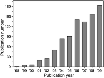 | ||
| Fig. 1 Statistic result of the publications with topic key words of “silver nanowire” or “silver nanowires” or “Ag nanowire” or “Ag nanowires” or “silver nanorod” or “silver nanorods” or “Ag nanorod” or “Ag nanorods” searched in the ISI Web of Science database. | ||
Silver has the highest electrical conductivity (6.3 × 10⁷ S·m−1) and thermal conductivity (429 W·m−1 · K−1) among all metals, resulting in that Ag powders have been widely used as conductive fillers of conductive adhesives3,4 and thermal interfacial materials5 widely used in electronics. Given the fact that Ag nanowires have thin diameters (usually < 100 nm) and large aspect ratios, percolation pathways can be easily formed even with very low load percentage of Ag nanowires, leading to significant reduction of Ag loading in comparison with the use of Ag particles as fillers.6 For example, the theoretical percolation threshold for randomly dispersed one-dimensional (1D) elongated particles with an aspect ratio of 1000 is 0.05 vol. %, while the threshold increases to 16 vol. % for spherical particles.7 In addition to dispersion in polymeric matrixes, Ag nanowires can also form two-dimensional (2D) random networks on supporting substrates, such as glass, plastic sheets, etc. with highly conductive percolation pathways to serve as conductive electrodes. The low percolation threshold for Ag nanowires assures that a conductive network has a high percentage of opening areas. In combination with the thin diameters of Ag nanowires, random networks of Ag nanowires represent a promising class of transparent conductive materials as replacement of doped metal oxides, most commonly tin-doped indium oxide (ITO).8–10 For instance, films of Ag nanowires (with average diameter and length of 84 nm and 6.6 μm, respectively) prepared using a cellulose-assisted transfer method have been demonstrated to exhibit the ratio of DC to optical conductivity, σDC/σop, approaching 500 when the film thickness is above ∼160 nm. The optimized films show optical transmittance of 85% and sheet resistance of 13 Ω/sq, which are comparable to the parameters of commercial ITO films (with optical transmittance and sheet resistance of 90% and ∼10 Ω/sq, respectively).10 Due to excellent mechanical flexibility of the Ag nanowires associated with their small lateral diameters, the transparent conductive films of Ag nanowires are very electromechanically robust, superior to the ITO films with fragility. This kind of nanowire films are expected to replace ITO films in applications such as solar cells, displays, touch panels, organic light-emitting diodes (OLED), etc. once the robust fabrication processes are developed to be compatible with the manufacture requirements.9,11
Similar to other nanostructures made of noble metals (e.g. Au and Ag), Ag nanowires exhibit strong surface plasmon resonances (SPRs) under photo-illumination due to strong coherent oscillation of free surface electrons in the nanowires, resulting in strong absorption and scattering of incident light.12–17 As a result, dispersions of Ag nanowires always display a yellowish color. The evanescent electrical fields near the surface of a Ag nanowire are usually very high, providing capability to enhance Raman scattering18,19 and fluorescence20,21 of molecules or emitters (such as quantum dots and upconversion nanocrystals) adjacent to the nanowires. For example, single Ag nanowire,22–24 randomly assembled networks,25 rafts of Ag nanowires assembled through Langmuir–Blodgett (LB) process26,27 and bundles of Ag nanowires28,29 have been evaluated to exhibit significant enhancement on Raman signals of molecules adsorbed on the surfaces of the Ag nanowires. Due to the anisotropic geometry of the Ag nanowires, the measured Raman scattering is strongly dependent on the polarization of excitation light.24,27,29 In addition, decorating surfaces of the Ag nanowires with metal nanoparticles can create “hot spots” (where the local electrical fields are drastically increased due to the strong coupling between the nanoparticles and nanowires) in the gaps formed between the nanowires and the nanoparticles for enhancing Raman scattering.24,30,31
In addition to SPRs, surface plasmon polaritons (SPPs) can be excited with free-space photons by coupling the energy into Ag nanowires and can propagate in the nanowires along their longitudinal axes.32–34 This property stimulates intensive interests in using Ag nanowires as waveguides in photonic and optoelectronic circuits because the confinement of photons/SPPs in the Ag nanowires with diameters less than 100 nm is not restricted by the diffraction limit. In contrast, it is always a problem in photonic waveguides when their dimensions are minimized down to sub-wavelength. Although Ag nanowires fabricated with varying methods including lithography can propagate SPPs, Ag nanowires synthesized through wet chemistry approaches exhibit much better performance with minimized losses due to their single crystallinity and atomic surface smoothness. In general, coupling photons into Ag nanowires to excite SPPs is challenging due to the dispersion relation mismatch for SPPs and photons. Photon momentum ħkx of a wave vector kx along the propagation direction ![[x with combining right harpoon above (vector)]](https://www.rsc.org/images/entities/i_char_0078_20d1.gif) , at a given photon energy ħω, is determined by ħω/c
, at a given photon energy ħω, is determined by ħω/c , where ħ is reduced Planck constant or Dirac constant, ω represents the angular frequency of the photon, c is speed of light in vacuum and ε0 represents the dielectric constant of the dielectric environment, and has to be increased by a ħΔkx to couple photons into SPPs. A number of strategies have been realized to couple external photons into Ag nanowires, for example, focusing a laser beam to the ends of a nanowire34 or landing an optical fiber taper on a nanowire (at either ends or midsection).35 Photons generated from emission of single-photon emitters (such as quantum dots, dye molecules)36,37 and ones propagated in photonic semiconductor nanowires/nanoribbons are also able to couple into Ag nanowires to excite SPPs, resulting in fabrication of hybrid nanophotonic components, such as polarization splitters, Mach-Zehnder interferometers, microring cavities, and optical routing networks.38,39 Conventional microscale polymer optical waveguides represent another class of examples that are capable of guiding photons to couple into Ag nanowires to realize the nanoscale confinement and guide light on a chip.40 All these results shed light on the promise in the use of chemically synthesized Ag nanowires as waveguides in optoelectronic circuits.
In combination of the guiding capability of Ag nanowires and “hot spots” created between the Ag nanowires and metal nanoparticles, surface-enhanced Raman scattering (SERS) of molecules on the Ag nanowires decorated with individual metal nanoparticles can be remotely excited by coupling external photons into the ends of the nanowires.41,42 In a typical measurement, a laser beam is focused to one end of a Ag nanowire to excite SPPs, which propagate in the nanowire and re-emit as photons at the points contacting with metal nanoparticles. These photons excite the SPRs in the Ag nanowire and the metal nanoparticles and their strong coupling results in strong local electrical field for SERS. The remote excitation of SERS in Ag nanowire/metal nanoparticle hybrid structures may be used as probes for potential high-resolution SERS imaging.
Properties and applications of Ag nanowires presented here (not limited to these examples) demonstrate the importance of Ag nanowires. In addition, Ag nanowires have been demonstrated to serve as a unique class of templates for synthesizing 1D nanoparticles with novel structures and functionalities, which are difficult (or impossible) to be synthesized via other methods. In this feature article, synthesis of Ag nanowires is first briefly reviewed with emphasis on polyol process, which is well established and widely used for large-scale production of Ag nanowires with pentagonal cross sections. The next section discusses the use of Ag nanowires as physical templates for fabricating metal/dielectric core/shell nanowires and dielectric nanotubes. In the following sections, chemical transformation of Ag nanowires (as chemical templates) to metal nanotubes with tunable wall morphologies, semiconductor nanowires, as well semiconductor-metal hybrid nanowires is discussed in details. Novel properties and applications associated with the newly derived nanostructures are also highlighted to address their importance. Finally, this article is concluded with personal perspectives to the potential applications of Ag nanowires and their derivatives.
2. Synthesis of Ag nanowires
Silver atoms usually crystallize into a face-centered cubic (fcc) structure although hexagonal close-packed (hcp) crystalline structure43–45 also exists in occasional cases, for example, single-crystalline 4H Ag nanowires can be synthesized via low–potential electrodeposition in porous membranes. As a result, formation of anisotropic Ag nanowires with fcc crystalline structure requires driving forces to break the cubic symmetry associated with the Ag lattice.46 Template-directed synthesis provides the most straightforward means for guiding the growth of Ag nanocrystals into nanowires either in cylindrical channels or against the existing 1D objects. Many kinds of templates have been successfully demonstrated by various research groups, and typical examples include step edges on the surfaces of solid substrates,47,48 channels within porous materials,2,49–51 mesoscale structures self-assembled from surfactants or block copolymers,52,53,54 biological macromolecules such as DNA strains,55–58 peptides/protein,59,60 or rod-shaped viruses,61 and 1D nanostructures (e.g. carbon nanotubes) synthesized using other methods.62 Although Ag nanowires as well as nanowires made of other metals can be synthesized with assistance of the aforementioned templates, the quality of the resulting nanowires usually needs to be improved in terms of crystallinity, surface smoothness, mass production, etc. for applications discussed in Introduction. In addition, the templates have to be fabricated prior to the synthesis of nanowires and have to be selectively removed (by chemical etching or calcination) in a post-synthesis process in order to harvest the nanowires, leading to tedious and time-consuming processes.On the other hand, chemical reduction of silver precursors (e.g. AgNO3) in homogenous liquid media with assistance of capping molecules, which can strongly bond to the side surfaces of Ag nanowires to facilitate their anisotropic growth and prevent the nanowires from aggregation. Creating the antisymmetric geometry in Ag nanowires during their growth always requires well separation of the sequential nucleation and growth steps.63,64 Nuclei formed at the nucleation stage have to present specific crystalline structures, such as five-fold multiple twinned configurations as discussed below, to initiate enlargement of the nuclei in an anisotropic mode at the growth stage. The differential bonding strength of the capping molecules towards side surfaces and end surfaces of the Ag nanowires provides additional driving force for the anisotropic growth. The better the two steps are separated, the better the quality and yield of the Ag nanowires are. Prof. Murphy and co-workers have pioneered a seed-mediated growth approach in which small Ag nanoparticles with sizes of ∼4 nm are pre-synthesized and added as seeds to a solution containing AgNO3, reductants, and surfactant molecules, such as cetyltrimethylammonium bromide (CTAB).65–67 This approach has been demonstrated to be successful in synthesizing Ag nanowires with well controlled aspect ratios. The Ag nanowires have been characterized with pentagonal cross sections, originating from the elongation of the five-fold multiple twinned seeds along the common axes.68–70 Other surfactant molecules (e.g. cetyltrimethylammonium tosylate, or CTAT;69 tetrabutylammonium bromide, or TBAB;71 sodium dodecyl sulfate, or SDS;72 dodecyl benzene sulfonic acid sodium, or DBS73) can also be used as capping agents for synthesis of Ag nanowires with similar quality. Nanoparticles with other shapes are always observed in these products and are ascribed to the fact that the crystalline structures of the seeds vary in a broad range. As a result, the purity of Ag nanowires can be significantly improved by using seeds with uniform five-fold multiple twinned structures. For example, uniform decahedral nanoparticles of Ag and Au have been recently synthesized through photochemical conversion of small Ag nanoparticles74–76 and reduction of HAuCl4 with diethylene glycol (DEG) with assistance of poly(vinyl pyrrolidone) (PVP),77 respectively. With these decahedral nanoparticles as seeds, Ag nanorods with precisely controlled aspect ratios and high purity have been synthesized through the well-established polyol process.78,79
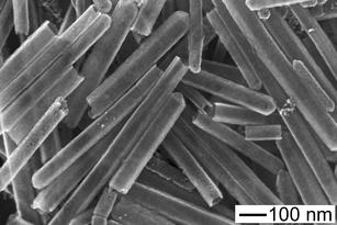
In addition to the seed-mediated two-step approaches, Ag nanowires have also been synthesized through one-pot reduction strategy, in which silver precursors are slowly added to reaction systems, for example, using syringe pumps. The Ag atoms generated at the very beginning of the reaction condense into nuclei with appropriate crystalline structures to serve as seeds for the further deposition of Ag atoms in the continuous reaction, leading to the growth of Ag nanowires. Polyol reduction of AgNO3 with assistance of polymeric surfactants, such as PVP, developed by Sun and Xia, represents one of the most successful method for the synthesis of high quality Ag nanowires in large quantity.80–83 This method sometimes is called self-seeding approach in comparison with the aforementioned seed-mediated approaches. In a typical synthesis as described elsewhere,82 3 mL ethylene glycol (EG) solution (0.1 M) of AgNO3 and 3 mL EG solution (0.6 M, calculated according to the molecular weight of repeating unit) of PVP (Mw ≈ 55 000) were simultaneously injected at a rate of ∼0.3 mL/min into 5 mL EG preheated in a three-neck flask immersed in an oil bath setting temperature at 160 °C using a two-channel syringe pump. The reaction mixture was further maintained at 160 °C for 60 min, resulting in an opaque gray solution with wispiness. The solution contained high concentration of Ag nanowires, as expected, as well as nanoparticles with other shapes (< 20%). Pure Ag nanowires were collected through centrifugation to remove the small volume nanoparticles. The sample (∼30 mg in each synthesis) shown in the scanning electron microscopy (SEM) image of Fig. 2A represents a typical example of purified Ag nanowires. These nanowires have diameters of ∼60 ± 8 nm and exhibit the straightness along the longitudinal axis and the level of purification. X-ray diffraction (XRD) pattern of these nanowires is well consistent with the fcc phase of silver. Similar to the nanowires synthesized in the seed-mediated approaches, the nanowires shown in Fig. 2A exhibit pentagonal cross section with D5h symmetry. Fig. 2B presents a transmission electron microscopy (TEM) image taken from a microtomed sample of the nanowires, clearly showing the five-fold symmetry. The non-pentagonal cross-sections are attributed to the random orientations of Ag nanowires relative to the edge of the microtome knife. The inset highlights the TEM image of a pentagonal cross-section, clearly revealing the five-fold contrast caused by twin boundaries. The sharp contrast across each twin plane indicates that each Ag nanowire contains five single crystalline subunits (labeled with T1, T2, T3, T4, and T5) and five equivalently flat side surfaces. As a result, no matter which one of the side surfaces lies against the surface of TEM grid during sample preparation, the TEM image always displays a twin boundary in the middle of a nanowire (see the typical TEM image of an individual nanowire shown in Fig. 2C). In particular, the twin boundaries (or twin planes) are straight and continuous along the entire longitudinal direction of each nanowire, indicating that the twin planes cannot twist and bend during the wire growth. By aligning electron beam perpendicular to one of the five side surfaces of the single Ag nanowire shown in Fig. 2C, typical selected-area electron diffraction (SAED) pattern is shown in Fig. 2D. This pattern indicates that each Ag nanowire is not a single crystal because the diffraction spots cannot be assigned to any particular simple pattern associated with fcc Ag. Instead, this pattern contains an interpenetrated set of two individual diffraction patterns, with the one in square symmetry corresponding to the [001] zone axis (from subunit of T1, inset of Fig. 2B) and the other one in rectangular symmetry to the [1![[1 with combining macron]](https://www.rsc.org/images/entities/char_0031_0304.gif)
![[2 with combining macron]](https://www.rsc.org/images/entities/char_0032_0304.gif) ] zone axis (from subunits of T3 and T4). The mutual orientation of these two zones induces the generation of double diffraction, which accounts for the remaining spots. The orientations of subunits of T2 and T5 are forbidden to diffract the incident electron beam. These assignments are also consistent with the results obtained for multiply twinned nanorods of Au and Cu having the same pentagonal symmetry.84,85 Analysis of this pattern also reveals that the side surfaces of the Ag nanowire are terminated by {100} facets and the longitudinal axis of the nanowire is along <110>.
] zone axis (from subunits of T3 and T4). The mutual orientation of these two zones induces the generation of double diffraction, which accounts for the remaining spots. The orientations of subunits of T2 and T5 are forbidden to diffract the incident electron beam. These assignments are also consistent with the results obtained for multiply twinned nanorods of Au and Cu having the same pentagonal symmetry.84,85 Analysis of this pattern also reveals that the side surfaces of the Ag nanowire are terminated by {100} facets and the longitudinal axis of the nanowire is along <110>.
![Characterization of Ag nanowires synthesized through a polyol process, in which AgNO3 was reduced with ethylene glycol with assistance of PVP. (A) SEM image of a random assembly of Ag nanowires purified via centrifuge. (B) TEM image of cross section of the Ag nanowires. The sample was prepared by dispersing and embedding the Ag nanowires in a cured epoxy matrix followed by slicing with microtome. (C) TEM image of an individual Ag nanowire, clearly showing the straightness of the twin plane (indicated by the arrow). (D) SAED pattern taken from the nanowire in (C) by aligning the electron beam perpendicular to one of the five side surfaces, clearly showing a superposition of patterns along [001] (square pattern labeled with solid lines) and [11̄2̄] (rectangular pattern labeled with dashed lines) zone axes for fcc Ag. The (220) and [2̄2̄0] reflections resulted in the same diffraction spots in the pattern. The pattern was reoriented for visional clarity. (E) Schematic illustration of growth mechanism of Ag nanowires with pentagonal cross sections from decahedrons. The surfactant molecules, PVP, selectively adsorb on the side {100} surfaces during the elongation of the decahedrons into nanorods and nanowires along the <110> crystalline direction.[Adapted with permission from ref. 80, Copyright 2003 American Chemical Society].](/image/article/2010/NR/c0nr00258e/c0nr00258e-f2.gif) | ||
| Fig. 2 Characterization of Ag nanowires synthesized through a polyol process, in which AgNO3 was reduced with ethylene glycol with assistance of PVP. (A) SEM image of a random assembly of Ag nanowires purified via centrifuge. (B) TEM image of cross section of the Ag nanowires. The sample was prepared by dispersing and embedding the Ag nanowires in a cured epoxy matrix followed by slicing with microtome. (C) TEM image of an individual Ag nanowire, clearly showing the straightness of the twin plane (indicated by the arrow). (D) SAED pattern taken from the nanowire in (C) by aligning the electron beam perpendicular to one of the five side surfaces, clearly showing a superposition of patterns along [001] (square pattern labeled with solid lines) and [1] (rectangular pattern labeled with dashed lines) zone axes for fcc Ag. The (220) and [0] reflections resulted in the same diffraction spots in the pattern. The pattern was reoriented for visional clarity. (E) Schematic illustration of growth mechanism of Ag nanowires with pentagonal cross sections from decahedrons. The surfactant molecules, PVP, selectively adsorb on the side {100} surfaces during the elongation of the decahedrons into nanorods and nanowires along the <110> crystalline direction.[Adapted with permission from ref. 80, Copyright 2003 American Chemical Society]. | ||
The characteristic results of the Ag nanowires grown through the polyol process indicates that each nanowire grown from a decahedral seed with assistance of PVP, as illustrated in Fig. 2E.80 As reported in previous work on synthesis of Ag colloids, decahedral nanoparticles with five-fold multiple twinned structures are popular in solution-based methods such as the polyol process.86 Each decahedral particle has a five-fold symmetry, with its surfaces bounded by ten {111} facets. It is believed that decahedral nanoparticles are formed at the beginning of the polyol reduction involved in the synthesis to serve as seeds to stimulate their enlargement into nanowires. Once the decahedral nanoparticles are formed, more Ag atoms formed from reduction condense and crystallize on the twin boundaries of the decahedral particles due to the high surface energies associated with the twin boundaries. This selective deposition of Ag atoms leads to the uniaxial elongation of decahedral nanoparticles into rod-shaped nanostructures under the confinement of twin planes. Because the twin planes do not twist or bend during the entire growth process, five straight edges along the longitudinal axis and five flat side surfaces of each wire are expected to be consistent with the observations. The newly formed side surfaces, {100} facets, must be stabilized through chemical interactions with the oxygen atoms of the pyrrolidone units of PVP.87 In comparison, the interaction between PVP and the {111} facets should be much weaker to enable the two ends of the nanorod to grow continuously. As a result, the pentagonal cross-section, the straightness of five side edges, and the flatness of five side surfaces are all kept throughout the growth process.
The polyol process has been successfully repeated in many academic and industrial laboratories for the synthesis of Ag nanowires even with a number of varieties, such as different polyols, PVP with different molecular weights, different surfactants (such as poly(vinyl alcohol), or PVA, ionic liquid), etc.88–90 However, purity of Ag nanowires in the final products varies when different batches of chemicals are used. Xia's group first pointed out the quality variation of Ag nanowires is related to impurities of the chemicals used in the synthesis. Quantitative analysis reveals that two major impurities in EG are Fe and Cl species and that their concentrations vary significantly from batch to batch to influence the formation of nuclei, and thus the yield and quality of Ag nanowires.91 Systematic studies indicate that Fe species regardless of its oxidation state can be reduced to Fe(II) by EG under the reaction conditions for nanowire synthesis. Fe(II) actively reacts with oxygen adsorbed on Ag nanocrystals and is oxidized into Fe(III), which can be reduced back to Fe(II) by EG. As a result, existence of Fe species in EG can consume oxygen in the reaction systems to prevent oxidation and dissolution of Ag nuclei during the nanowire synthesis. On the other hand, Cl species, always in the form of Cl− ions, has strong coordination affinity towards Ag+ ions and thus accelerate oxidation and dissolution of Ag nuclei in the presence of oxygen. Apparently, the influence of Fe and Cl species on the stability of Ag nuclei is competitive. As discussed previously, the nuclei for nanowire growth are Ag nanoparticles with five-fold multiple twinned structures. The crystalline defects associated with the multiple twinned structures are more active to react with Cl− ions if oxidant (such as oxygen) is present, leading to dissolution of the multiple twinned nanoparticles. On the other hand, nanoparticles with single crystallinity can tolerate the existence of Cl− ions. As a result, coexistence of high concentration Cl− ions and oxygen is not favorable for the growth of Ag nanowires. In contrast, either removal of oxygen from reaction system91 or addition of appropriate amount of Fe species92 can help the synthesis of Ag nanowires with high yield. Comprehensive understanding on the effect of impurities (i.e. Fe and Cl species) stimulates researchers' interests in studying the influence of ionic additives on the morphologies of Ag nanoparticles and opens a new avenue for shape-controlled synthesis of metal nanoparticles.93–104
Similar to the synthesis of Ag nanowires templating against the existing 1D structures, Ag nanowires can also serve as physical templates to guide the growth of 1D nanostructures made of other materials, such as dielectric sheaths outside the Ag nanowires. Due to the chemical reactivity of Ag towards strong oxidants, Ag nanowires can also be used as sacrificial chemical templates for the synthesis of 1D nanostructures which are difficult to be available through conventional synthetic approaches, for example, metal nanotubes and silver halide nanowires. The following sections present the synthetic strategies with the use of Ag nanowires as templates and typical examples as well as their applications in photonics and catalysis.
3. Synthesis of metal/dielectric core/shell nanowires: Ag nanowires as physical templates
Silver nanowires synthesized through the aforementioned approaches are usually stable and well dispersed in varying solvents because their surfaces can be easily modified with different molecules, which provide appropriate surface affinity compatible for deposition of dielectric materials. Fig. 3 depicts the strategy for making metal/dielectric core/shell nanowires (or nanocables) and dielectric nanotubes by using Ag nanowires as physical templates. First, Ag nanowires with appropriate surface modification are dispersed in a solution containing precursor(s) which can react to deposit dielectric layers outside of the Ag nanowires, resulting in Ag nanowire/dielectric core/shell structures. In the next step, the dielectric coating can be partially removed to expose the ends of the Ag nanowires to form nanocables, which are expected to serve as interconnects in nanoscale electronic circuitries. In contrast, selectively dissolving the Ag nanowire cores with chemical etchant, such as ammonia hydroxide, nitric acid, etc., results in dielectric nanotubes.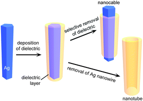 | ||
| Fig. 3 Schematic illustration depicting the use of Ag nanowires synthesized through the polyol process as physical templates for synthesizing Ag/dielectric core/shell nanowires and other derivate nanostructures including nanocables and dielectric nanotubes, which are synthesized by selective removal of partial dielectric sheaths and inner Ag cores, respectively. | ||
Nanowires made of Ag as well as other metals (such as Au) have been successfully coated with dielectric materials including SiO2,105–108 TiO2,109 polystyrene.110 Wettability of the nanowire surfaces towards the dielectric coating is critical to the success in the synthesis of core/shell nanowires. For the case of SiO2 coating, a primer (e.g. amine- or mercapto-terminated oxysilane molecules) is usually applied to replace the existing surfactant layers of the chemically synthesized nanowires106 or bond to the bare surfaces of nanowires synthesized with templates.107 The amine or mercapto group can strongly bond to the surfaces of Ag nanowires while the siloxane moiety reacts with the precursor (such as tetraethyl orthosilicate, or TEOS) of SiO2 during the hydrolysis process:
| Si(OC2H5)4 + 2H2O → SiO2 + 4C2H5OH | (1) |
![(A–E) TEM images of Ag/SiO2 core/shell nanowires prepared by coating the Ag nanowires shown in Fig. 2A with conformal SiO2 sheaths through a sol–gel reaction involved with hydrolysis of TEOS under different conditions: (A) concentration of TEOS of 0.0375 M and reaction time of 45 min; (B–E) concentration of TEOS of 0.072 M and reaction time of (B) 5, (C) 10, (D) 30, and (E) 45 min. (F) TEM image of three Ag/SiO2 core/shell nanowires (as shown in (A)) where the Ag cores were partially dissolved by the ammonia (highlighted by the arrows) used in the sol–gel reaction. (G) TEM image of SiO2 nanotubes obtained by completely dissolving the Ag cores with ammonia. [Adapted with permission from ref. 105, Copyright 2002 American Chemical Society].](/image/article/2010/NR/c0nr00258e/c0nr00258e-f4.gif) | ||
| Fig. 4 (A–E) TEM images of Ag/SiO2 core/shell nanowires prepared by coating the Ag nanowires shown in Fig. 2A with conformal SiO2 sheaths through a sol–gel reaction involved with hydrolysis of TEOS under different conditions: (A) concentration of TEOS of 0.0375 M and reaction time of 45 min; (B–E) concentration of TEOS of 0.072 M and reaction time of (B) 5, (C) 10, (D) 30, and (E) 45 min. (F) TEM image of three Ag/SiO2 core/shell nanowires (as shown in (A)) where the Ag cores were partially dissolved by the ammonia (highlighted by the arrows) used in the sol–gel reaction. (G) TEM image of SiO2 nanotubes obtained by completely dissolving the Ag cores with ammonia. [Adapted with permission from ref. 105, Copyright 2002 American Chemical Society]. | ||
Because of the existence of ammonia in the sol–gel reaction media with a pH of 10.5–11, the Ag cores in the core/shell nanowires are not stable under ambient environment due to the dissolution reaction:
| 4Ag + O2 + 8NH3·H2O → 4Ag(NH3)2+ + 4OH− + 6H2O | (2) |
Experimental observations reveal that the Ag cores start to be dissolved if the sol–gel reaction lasts longer than 45 min, leaving the peapod-like structures (Fig. 4F). When the reaction time is long enough, the Ag cores are completely dissolved, resulting in formation of uniform SiO2 nanotubes (Fig. 4G). As a result, the as-synthesized Ag/SiO2 core/shell nanowires have to be separated from the reaction solution once the SiO2 shells with desired thickness have been grown and re-dispersed in DI water or other solvents where both Ag and SiO2 could survive. In addition, metal etchants (for example, concentrated HNO3 or NH3 for Ag; KCN for Au) can be added to stable dispersions of metal/dielectric core/shell nanowires to selectively dissolve the metal cores, leaving the formation of pure nanotubes made of different dielectric materials.105,110,111
The as-synthesized Ag/SiO2 core/shell nanowires can be used as nanoscale cables because of the high conductivity of Ag (6.3 × 10⁷ S·m−1) and high electrical resistance of SiO2 (1 × 10¹⁶ Ω·m). Challenges include exposure of the ends of Ag nanowires by partially removing SiO2 coating and integration of the nanocables with nanoscale electronic and optoelectronic units, such as transistors, diodes, logic gates, etc.112–115 The SiO2 nanotubes shown in Fig. 4G might serve as carriers for interesting species, such as drugs, because of their wall porosity and void interiors. Diffusion rate could be controlled by changing the thickness of the nanotubes. Most recently, Yin and co-workers have developed a “surface-protected etching” methodology to etch the sol–gel derived SiO2 layers by using PVP as protecting ligand and NaOH as etchant, resulting in thinned and mesoporous SiO2 shells.116–118 The thinning effect leads to the formation of void spaces between SiO2 shells and the inner metal cores, resulting in the surfaces of the metal cores be accessible to the environmental species diffused through the mesopores in the SiO2 shells. In combination with the stability of SiO2 nanostructures under many reaction conditions, the metal core/mesoporous SiO2 shell nanostructures can serve as nanoreactors and high-efficient catalysts.119
4. Synthesis of metal nanotubes: Ag nanowires as chemical templates
As pointed out in the previous section, Ag nanowires can react with other chemicals and serve as chemical templates, leading to the formation of 1D nanostructures made of other materials. For example, galvanic displacement reactions between Ag nanowires and precursors of more noble metals (e.g. Au, Pt, Pd) result in the formation of metal nanotubes which are difficult to be synthesized through conventional approaches.120 Good dispersity of Ag nanowires in appropriate solvents is critical to synthesize metal nanotubes with high quality in terms of crystallinity, well-defined morphology, and good dispersibility. In general, colloidal Ag nanowires synthesized with assistance of surfactant molecules disperse very well in the reaction solutions since their surfaces are coated with the surfactant molecules. On the other hand, surfaces of the nanowires formed with assistance of templates are usually lack of surfactant molecules, leading them to be difficult to well disperse in appropriate solvents for chemical transformation.4.1. Galvanic displacement reaction between Ag nanowires and HAuCl4
Since the standard reduction potential of AuCl4−/Au pair (0.99 V vs. standard hydrogen electrode, SHE) is higher than that of Ag+/Ag pair (0.80 V vs. SHE), Ag can be oxidized into Ag+ when an aqueous solution of HAuCl4 is added to an aqueous suspension of Ag nanowires:| 3Ag + AuCl4− → Au + 3Ag+ + 4Cl− | (3) |
Fig. 5 illustrates the major steps involved in the galvanic reaction between Ag nanowires and HAuCl4 that is performed at the boiling temperature of water, i.e. 100 °C. After the HAuCl4 solution is added to the dispersion of Ag nanowires as shown in Fig. 2, the displacement reaction starts from the sites with relatively high surface energies (typical examples include steps, point defects, and stacking faults) of the side {100} surfaces.121 Once the reaction starts on the active sites of each nanowire, the Ag atoms in the nanowire will continue to dissolve because etching generates new surfaces with even more higher surface energies.122 Meanwhile, the elemental Au generated in the reaction tends to be epitaxially deposited on the surface of each nanowire because of a good matching between the crystalline structures (fcc lattice for both Au and Ag) and lattice constants (4.0786 and 4.0862 Å for Au and Ag, respectively, with only 0.186% difference). As highlighted in the bottom of Fig. 5, the displacement behaves as a corrosion process, with Ag being oxidized at the anode. The released electrons migrate to the entire surface of the nanowire to reduce AuCl4− ions into Au atoms (cathode reaction). The deposition leads to the formation of an essentially complete, thin layer of Au with only several holes at the initial reaction sites (step A). The Au coating prevents the underneath Ag from directly contacting and reacting with AuCl4− ions. As a result, the etching of Ag nanowire continues at the newly formed surfaces as shown in the illustration of cross section and the resulting Ag+ ions continue to diffuse out of the cavities through the small holes. When the concentration of HAuCl4 is high enough, the dissolution of Ag transforms each Ag nanowire into a structure characterized by a hollow interior, i.e. nanotube (step B). Along with the displacement reaction between the Ag nanowires and HAuCl4, alloying spontaneously occurs between the deposited Au layer and the underlying Ag surface because the diffusion rates of Ag and Au atoms are relatively high at 100 °C123 and the homogeneous Au-Ag alloy is more stable than either pure Au or Ag.124 The formation of alloyed walls is important to process them into nanotubes with pores through dealloying process.125 Addition of Ag etchant can selectively dissolve Ag out to leave porous Au nanotubes.126 Alternatively, if more HAuCl4 react with the Au-Ag alloy nanotubes, the Ag atoms in the nanotubes can also be selectively taken out. In this dealloying process, numbers of lattice vacancies are formed because only one Au atom is generated at the expense of three Ag atoms, according to the stoichiometric relationship shown in eqn (3). The reduced mass density generates negative curvatures into the solid walls of the nanotubes, and thus increases their interfacial area and surface energy.127 Refluxing the aqueous dispersion of nanotubes releases these defects and reconstructs the morphology of the nanotubes via Ostwald ripening process, resulting in the formation of many pinholes in the walls (step C).128 Further dealloying enlarges the lateral dimensions of the pinholes and many adjacent ones coalesce into larger ones (step D). It is interesting to note that these large holes tend to form square (or rectangular) profiles once their dimensions have reached a critical value (∼20 nm). The specific shape of these pores might be related to the square arrangement of atoms on each side wall where the surface is mainly bounded by {100} crystallographic planes. Complete dealloying causes the porous nanotubes to collapse into small fragments of pure Au (step E).
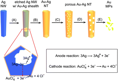 | ||
| Fig. 5 Schematic illustration highlighting the morphological evolution of a Ag nanowire involved in the galvanic displacement reaction between the Ag nanowire and an aqueous solution of HAuCl4 at 100 °C. The major steps include: (A) initiation of displacement reaction at a specific site with relatively high surface energy, or several sites for long wires; (B) continuation of the reaction and formation of a nanotube with smooth and uniform wall composed of Au-Ag alloy; (C) initiation of dealloying process and the formation of small pinholes in the nanotube wall; (D) continuation of dealloying with the formation of square (or rectangular) holes in the wall; (E) fragmentation of the porous nanotube into Au nanoparticles with irregular shapes triggered by complete (or deep) dealloying. The cross section highlights the microscopic view of galvanic displacement reaction that includes i) oxidation and dissolution of Ag; ii) diffusion of Ag+ ions out of the cavity; iii) diffusion of AuCl4− ions to the outer surface of the nanowire; and iv) reduction of AuCl4− ions and deposition of Au on the nanowire. NW, NT, and NPs represent nanowire, nanotube, and nanoparticles, respectively. | ||
Given the low solubility of AgCl in water, the formation of AgCl solid has to be considered because the crystallization of metallic surfaces might be influenced by the simultaneous precipitation of AgCl. The solubility product (ksp) of AgCl is ∼1.8 × 10⁻¹⁰ in cold water at 20 °C. When the temperature increases to 100 °C, ksp increases accordingly to ∼1.2 × 10⁻⁶ because the dissolution process has a positive enthalpy (ΔH0 = 65.57 kJ/mol). As a result, concentration of Ag nanowires should be lower than a critical value in order to avoid the formation of AgCl solid during displacement reaction. On the other hand, white solid appears at the bottom of the reactor when the reaction mixture is cooled down to room temperature, indicating precipitation of AgCl. The well separation between displacement reaction and AgCl precipitation prevents the Au-Ag alloy nanotubes from being contaminated by AgCl and also helps to maintain the epitaxial growth of Au shells on Ag nanowires for the formation of highly crystalline nanotubes. If necessary, the AgCl precipitate can be easily dissolved either with a saturated NaCl solution through the coordination reaction:129
| AgCl + 3Cl− → AgCl43− | (4) |
| AgCl + 2NH3·H2O → Ag(NH3)2+ + Cl− + 2H2O | (5) |
The metal nanotubes can be readily collected as a pure sample through centrifugation, and then re-dispersed in water for further surface modification and application.130
4.2. Morphological and structural evolution in the reaction
Both SEM and TEM have been used to track the morphological and structural variations involved in the displacement reaction between Ag nanowires and HAuCl4. As shown in Fig. 2, each Ag nanowire synthesized through the polyol process has a pentagonal cross-section, five straight side edges parallel to its long axis, five flat side surfaces bounded by {100} facets, ten {111} end facets, and a multiple twinned crystalline structure of five-fold symmetry.80 Reacting a same amount (i.e. 4.3 mmol in terms of elemental Ag) of Ag nanowires (Fig. 6A) with a 1 mM HAuCl4 solution results in nanowires/nanotubes with different morphologies depending on the volume of HAuCl4 solution. Frames B–F of Fig. 6 present typical TEM images of the resulting nanostructures, in accord well with the major steps highlighted in Fig. 5. When a small volume, e.g. 0.3 mL, of HAuCl4 solution is used, each Ag nanowire develops interior cavities (i.e. tubular strips) (Fig. 6B). All the Ag nanowires are transformed into continuous nanotubes with smooth and uniform walls once the volume of HAuCl4 solution is increased to a critical value, i.e. 0.6 mL (Fig. 6C). It is worth noting that each nanotube inherits all the morphological features of the Ag nanowires, such as pentagonal cross section, five straight side edges, and five flat side surfaces (right top inset of Fig. 6C). Electron diffraction patterns (bottom left inset of Fig. 6C) taken from individual nanotubes are essentially the same as those of the Ag nanowires. The morphological and structural consistence between the Ag nanowires and the resulting nanotubes further confirms that the elemental Au generated from the displacement reaction is epitaxially deposited on the surfaces of the Ag nanowires. Dealloying of these Au-Ag alloy nanotubes with more HAuCl4 solution leads to the formation of pores in their walls (Fig. 6D and 6E). The pore size is dependent on the volume of HAuCl4 that is added to the dispersion of Ag nanowires. The inset SEM images clearly show that the profiles of small holes are almost circular and the larger holes (with sizes >20 nm) display a square symmetry. Complete dealloying of the alloy nanotubes eventually results in the formation of Au nanoparticles with irregular shapes (Fig. 6F).![TEM images taken from Ag nanowires (A) before and (B–F) after they reacted with different volumes of 1 mM HAuCl4 aqueous solution at 100 °C: (B) 0.3, (C) 0.6, (D) 1.5, (E) 2.3, and (F) 3.0 mL. The top right insets in (C–E) are the SEM images of the resulting nanotubes with different wall morphologies: (C) smooth and continuous walls, (D) walls with small pinholes with sizes less than 5 nm, and (E) walls with square and rectangular holes with sizes larger than 20 nm. The bottom left inset of (C) represents a typical SAED pattern taken from an individual nanotube by aligning the electron beam perpendicular to one of the five side surfaces. [Adapted with permission from ref. 120, Copyright 2004 American Chemical Society].](/image/article/2010/NR/c0nr00258e/c0nr00258e-f6.gif) | ||
| Fig. 6 TEM images taken from Ag nanowires (A) before and (B–F) after they reacted with different volumes of 1 mM HAuCl4 aqueous solution at 100 °C: (B) 0.3, (C) 0.6, (D) 1.5, (E) 2.3, and (F) 3.0 mL. The top right insets in (C–E) are the SEM images of the resulting nanotubes with different wall morphologies: (C) smooth and continuous walls, (D) walls with small pinholes with sizes less than 5 nm, and (E) walls with square and rectangular holes with sizes larger than 20 nm. The bottom left inset of (C) represents a typical SAED pattern taken from an individual nanotube by aligning the electron beam perpendicular to one of the five side surfaces. [Adapted with permission from ref. 120, Copyright 2004 American Chemical Society]. | ||
4.3. Compositional variation of nanostructures in the reaction
Compositional survey of the nanostructures formed during the displacement reaction between the Ag nanowires and HAuCl4 with energy dispersive X-ray (EDX) spectroscopy indicates that the resulting nanotubes are composed of both Au and Ag regardless of their exact morphologies. Inductively coupled plasma atomic emission spectroscopy (ICP-AES) has been used to precisely analyze the percentage of Au and Ag in the nanostructures that are prepared by reacting the same amount of Ag nanowires with different volumes of 1 mM HAuCl4 solution. The use of inductively coupled plasma (ICP) can directly atomize the metal nanostructures because its flame can reach a temperature as high as 9000 K.131 As a result, dissolution of metal nanostructures with strong acids and strong oxidants can be avoided without scarification of the measurement precision. The molar percentages of Au in a set of products are shown in Fig. 7. The result indicates that more Au is generated as more HAuCl4 is added to the dispersion of Ag nanowires. At the early stage of the reaction, i.e. the volume of HAuCl4 solution less than ∼0.75 mL, the measured percentages (symbols) of Au are consistent with the calculated values (dashed curve) according to the stoichiometric relationship shown in eqn (3). If the stoichiometric relationship remains throughout the entire displacement reaction, 1.43 mL of 1 mM HAuCl4 solution could completely oxidize the Ag nanowires into Ag+ ions. However, experimental data indicates that much more HAuCl4 solution is required to reach this point, and this volume is as high as 3.0 mL. The difference is ascribed to that the dealloying process seems to need HAuCl4 with much higher chemical potentials, thus higher concentrations, to selectively take the Ag atoms out from the alloy matrix. Comparison of the experimental data with the calculated data indicates that HAuCl4 mainly reacts with the pure Ag at the early stage, i.e. with small volume (< 0.7 mL) of HAuCl4 solution. The conclusion is consistent with the schematic illustration highlighted in the bottom of Fig. 5, i.e. HAuCl4 only reacts with the pure Ag cores rather than the Au-Ag alloy surfaces because pure Ag is more reactive than the alloyed Ag. Once the Au-Ag alloy nanotubes with continuous, uniform walls are formed, addition of more HAuCl4 starts to dealloy the nanotubes along with morphological reconstructions. The molar percentage of Au reaches 96.5% when the volume of HAuCl4 solution is increased to 3.0 mL, confirming that the nanoparticles (as shown in Fig. 6F) obtained as the final product of the displacement reaction are essentially composed of pure Au.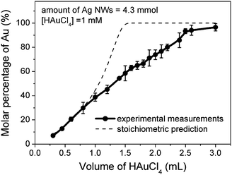 | ||
| Fig. 7 Dependence of the molar percentage of Au in the resulting nanostructures obtained through the reaction between Ag nanowires and an aqueous solution of 1mM HAuCl4 on its volume. | ||
4.4. Spectral evolution involved in the reaction
Similar to Ag nanowires, nanostructures derived from the displacement reactions between Ag nanowires and HAuCl4 also exhibit intense absorption and scattering due to their strong SPRs. Fig. 8 plots the absorption spectra of the nanostructures as shown in Fig. 6, showing that the major peaks vary in the UV-visible-near infrared (NIR) spectral region depending on the volume of the HAuCl4 solution added to the dispersion of Ag nanowires. Specifically, the dispersion of Ag nanowires exhibits only one major peak around 380 nm, which originates from the transverse mode of SPR.81 When they react with small amount (< 0.6 mL) of HAuCl4 and are partially converted to tubular nanostructures (as shown in Fig. 6B), this peak slightly red-shifts due to the formation of Au-Ag alloy sheath on the surface of each nanowire (Fig. 8A). An additional peak located at wavelength larger than 600 nm is gradually formed, which is attributed to the transverse mode of newly formed tubular strips. As the volume of HAuCl4 solution is increased to 0.6 mL, the typical SPR peak of the Ag nanowires essentially disappeared, indicating that the Ag nanowires are completely transformed into nanotubes. The peak at longer wavelength blue-shifts back to 655 nm, implying that the wall thickness of the nanotubes increases as the displacement reaction continues. When the Ag nanowires react with HAuCl4 solution more than 0.7 mL, dealloying process occurs to thin the walls of the Au-Ag alloy nanotubes as well as to create holes in the walls, leading their SPR peak to further red-shift to 930 nm (Fig. 8B and C). The nanotubes start to collapse into pure Au nanoparticles with fingerprint SPR peak around 520 nm when the volume of HAuCl4 solution is higher than 2.3 mL (red curve in Fig. 8C). Reaction with more HAuCl4 (> 2.5 mL) finally destructed all the nanotubes to form Au nanoparticles. As a result, by controlling the displacement reaction between Ag nanowires and HAuCl4, the SPR peak of the resulting nanotubes can be tuned in the range from 655 to 930 nm before they collapse into Au nanoparticles (Fig. 8D). The high absorption coefficient of the nanotubes in the NIR region (800–1200 nm, the transparent window of soft tissues) may find medical applications such as contrast-enhanced imaging,130,132–135 photothermal cancer therapy,134,136–138 and remotely photothermally triggered drug release.139,140 The large dimensions (from several microns to tens of microns) along the longitudinal axes of the nanotubes might be problematic in the envisioned applications. This limitation can be solved by mechanically breaking the nanotubes down to short segments through ultrasonication. Fig. 9 presents a typical SEM image of such broken nanotubes, clearly showing their lengths (< 1 μm) much shorter than the original nanotubes shown in Fig. 6. Their lengths can be further decreased by increasing the sonication time and power. Decrease in the nanotube length does not change their SPR absorption peak in the visible-NIR region because the peak is ascribed to the transverse SPR mode (i.e. characteristic of their cross sections) of the nanotubes, thus does not affect the aforementioned potential applications.![(A–C) UV-visible-NIR absorption spectra of Ag nanowires (all in the same amount) before and after they reacted with different volumes of 1 mM HAuCl4 aqueous solution. The numbers listed in each panel represent the volume of HAuCl4 solution added to react with the Ag nanowires. All spectra were normalized against the intensities of the strongest peaks. (D) Absorption peak position of the nanotubes as a function of the volume of HAuCl4 solution. [Adapted with permission from ref. 120, Copyright 2004 American Chemical Society].](/image/article/2010/NR/c0nr00258e/c0nr00258e-f8.gif) | ||
| Fig. 8 (A–C) UV-visible-NIR absorption spectra of Ag nanowires (all in the same amount) before and after they reacted with different volumes of 1 mM HAuCl4 aqueous solution. The numbers listed in each panel represent the volume of HAuCl4 solution added to react with the Ag nanowires. All spectra were normalized against the intensities of the strongest peaks. (D) Absorption peak position of the nanotubes as a function of the volume of HAuCl4 solution. [Adapted with permission from ref. 120, Copyright 2004 American Chemical Society]. | ||
 | ||
| Fig. 9 SEM image of broken Au-Ag alloy nanotubes prepared through ultrasonication of nanotubes as shown in Fig. 6C. | ||
4.5. Galvanic displacement reaction between Ag nanowires and other metal precursors
In addition to HAuCl4, Ag nanowires can also be oxidized by Pt2+ and Pd2+ ions through similar galvanic displacement reactions because the standard reduction potentials of these two metals are higher than that of Ag+/Ag pair, i.e. ∼1.2 V (vs. SHE) for the Pt2+/Pt pair and 0.83 V (vs. SHE) for the Pd2+/Pd pair:141| 2Ag + Pt2+ → 2Ag+ + Pt | (6) |
| 2Ag + Pd2+ → 2Ag+ + Pd | (7) |
For example, refluxing Ag nanowires with an aqueous solution of Pt(CH3COO)2 for 30 min results in the formation of Pt-Ag alloy nanotubes with high yield (see Fig. 10A for a typical TEM image). Their walls are rough and primarily composed of discrete nanodomains, significantly different from the smoothness of the Au-Ag alloy nanotubes shown in Fig. 6C. This difference might be ascribed to the larger mismatch (4.2%) of the lattice constant between Pt and Ag (3.920 Å vs. 4.0862 Å), leading to difficulty for epitaxial deposition. Reaction of Ag nanowires with an aqueous solution of Pd(NO)2 produces nanotubes made of Pd-Ag alloys, also showing roughness of their walls (Fig. 10B). Mismatch of the lattice constant between Pd and Ag (3.890 Å vs. 4.0862 Å) is even larger, i.e. 5.0%, which corresponds to the wall roughness. Nanostructures made of Pd and Pt as well as their alloys have been proven a promising class of catalysts in many applications, such as fuel cells, batteries, and chemical industries.142–147 The hollow interiors of the alloy nanotubes shown in Fig. 10A and B enable the nanotubes to expose more surface areas to catalyze reactions in comparison with their solid counterparts, i.e. nanowires, thus exhibit better catalytic performance. Ag atoms in the alloy nanotubes can be selectively dissolved to leave the nanotubes made of pure Pd or Pt with even higher surface areas due to the formation of nanoscale pores in the nanotube walls.148 We tested the as-synthesized Pd-Ag alloy nanotubes (shown in Fig. 10B) as catalysts for the Suzuki coupling reaction between phenylboronic acid and iodobenzene with yield approaching 100%.141 Their catalytic performance decreases after the first use because the surfaces of the nanotubes are coated with products during reaction. Coating the nanotubes with porous protecting layers, such as SiO2, may eliminate the poisoning effect of the reaction products.
![(A) TEM image of Pt-Ag alloy nanotubes synthesized through reaction of Ag nanowires with Pt(CH3COO)2 in boiling aqueous solution. (B) TEM image of Pd-Ag alloy nanotubes prepared through refluxing Ag nanowires with Pd(NO3)2 aqueous solution at 100 °C. [Adapted with permission from ref. 141, Copyright Wiley-VCH Verlag GmbH & Co. KGaA.] (C) TEM image of Ag nanowires coated with a thin layer of Pd-Ag alloy sheath through a shallow displacement reaction of Ag nanowires with Pd(NO3)2. (D) PC isotherms for hydrogen desorption from the hydrides of the Ag/Pd-Ag core/shell nanowires shown in (C) at 20, 70, and 120 °C. H/M represents the hydrogen-to-metal molar ratio. [Adapted with permission from ref. 149, Copyright 2004 American Chemical Society].](/image/article/2010/NR/c0nr00258e/c0nr00258e-f10.gif) | ||
| Fig. 10 (A) TEM image of Pt-Ag alloy nanotubes synthesized through reaction of Ag nanowires with Pt(CH3COO)2 in boiling aqueous solution. (B) TEM image of Pd-Ag alloy nanotubes prepared through refluxing Ag nanowires with Pd(NO3)2 aqueous solution at 100 °C. [Adapted with permission from ref. 141, Copyright Wiley-VCH Verlag GmbH & Co. KGaA.] (C) TEM image of Ag nanowires coated with a thin layer of Pd-Ag alloy sheath through a shallow displacement reaction of Ag nanowires with Pd(NO3)2. (D) PC isotherms for hydrogen desorption from the hydrides of the Ag/Pd-Ag core/shell nanowires shown in (C) at 20, 70, and 120 °C. H/M represents the hydrogen-to-metal molar ratio. [Adapted with permission from ref. 149, Copyright 2004 American Chemical Society]. | ||
As highlighted in step A of Fig. 5, shallow displacement reaction between Ag nanowires and Pd(NO3)2 forms core/shell nanowires with a number of small cavities, which are composed of thin Pd-Ag alloy shells and Ag cores. Fig. 10C presents a typical TEM image of such coaxial core/shell nanowires containing only 7.8% Pd (calculated from the EDX data as shown in the inset). Similar to the continuous Pd-Ag alloy nanotubes in Fig. 10B, the Pd-Ag alloy shells of the nanowires shown in Fig. 10C are also rough and constructed with many small nanodomains (< 10 nm). Most interestingly, the pressure-composition (PC) isotherms, which are usually used to characterize the thermodynamics of metal-hydrogen systems, of the core/shell nanowires shown in Fig. 10C are similar to that of polycrystalline Pd powders with sizes of ∼3 nm.149Fig. 10D plots the PC isotherms at 20, 70, and 120 °C, clearly showing the existence of distinct plateaus and broad metal-H miscibility gaps. For example, the hydrogen solubilities at α/(α + β) and (α + β)/β phase boundaries at 20 °C are 0.11 and 0.64 H/M (i.e. hydrogen-to-metal molar ratio), respectively, for the as-synthesized core/shell nanowires, while these values are 0.008 and 0.61 H/M, respectively, for Pd powders. The higher concentration of hydrogen at the α/(α + β) boundary for the core/shell nanowires might be ascribed to that dissociation of H2 to H on Pd-Ag alloy shells is more difficult than on pure Pd nanoparticles and/or diffusion of H from Pd-Ag alloy shells into the lattice of pure Ag cores is harder than diffusion within pure Pd lattice of Pd powders. The adsorption and desorption of hydrogen are reversible and reaction rates are very high even at room temperature. For instance, the complete desorption at 20 °C takes about 10 min. The high solubility of hydrogen in the Ag nanowires coated with Pd-Ag alloy sheaths is attributed to the formation of the thin Pd-Ag alloy layer because hydrogen is not soluble in pure Ag.150 Nanotubes and nanowires made of pure Pd synthesized via template-assisted method151 exhibit the similar capability to the core/shell nanowires of Fig. 10C, indicating that the cavities in the core-shell nanowires do not response for the hydrogen adsorption. This similarity also indicates that the mechanism of hydrogen storage in metallic nanostructures is mainly determined by the formation of hydride rather than physisorption and capillary effects associated with the tubular morphology. In addition, the composite core/shell nanowires exhibit a significant enhancement in mechanical strength during hydrogen adsorption/desorption process. For example, the composite nanowires only slightly bend or break at some points of cavities after 50 cycles of hydrogen adsorption/desorption, while the pure Pd nanotubes and nanowires collapse into particles only after 25 cycles.149 Study on the kinetics of hydrogen adsorption and desorption in the Ag/Pd-Ag core/shell nanowires with very low content of Pd can help us to achieve a better understanding of hydriding/dehydriding processes as well as to develop low-cost, safer materials for related applications, such as hydrogen storage.
4.6. Multiple-walled nanotubes made of metals
The Au-Ag alloy nanotubes shown in Fig. 6C can also serve as physical templates for deposition of Ag on their outside surfaces through electroless plating, in which Ag+ ions are reduced with conventional reducing agents, such as ascorbic acid. Applying galvanic displacement reaction of Fig. 5 to the Ag-coated nanotubes can generate double-walled nanotubes.152Fig. 11A schematically outlines the major steps involved in the fabrication of multiple-walled nanotubes composed of Au-Ag alloy. In the first step (i), mixing Ag nanowires with an aqueous HAuCl4 solution induces the galvanic displacement reaction (eqn (3)) and forms Au-Ag alloy nanotubes (detailed discussion in section 4.1). Due to good matching of lattice constant between Au and Ag, electroless plating of Ag on the surfaces of the Au-Ag alloy nanotubes forms conformal sheath of Ag with thickness determined by the reaction parameters including concentration of Ag+ ions and reducing agents as well as plating time (step ii). After repeating the galvanic displacement reaction with HAuCl4, new tubular walls with larger lateral dimensions are formed, resulting in double-walled nanotubes (step iii). Coaxial nanotubes with more than two walls can be readily synthesized by repeating steps (ii) and (iii). Fig. 11B shows a typical SEM image of a sample of double-walled nanotubes with both walls made of Au-Ag alloy. The inset highlights the cross-section of one nanotube, clearly showing a pentagonal profile for both inner and outer tubes and coaxial relationship (Fig. 11C). The double-walled nanotubes exhibit the same electron diffraction pattern (Fig. 11D) as that taken from a Ag nanowire (Fig. 2D) or a single-walled Au-Ag nanotube (inset of Fig. 6C), indicating that the epitaxial relationship is well maintained throughout both electroless plating and displacement reactions. Synthesis of multiple-walled nanotubes made of three Au-Ag alloy walls is also successful and Fig. 11E presents a typical SEM image of such nanotubes. The tube fractured at its end clearly shows its triple-walled structure. If the precursor is switched from HAuCl4 to Pd(NO3)2 in the second displacement reaction (i.e. step iii of Fig. 11A), double-walled nanotubes made of hybrid compositions can be prepared. Fig. 11F shows an SEM image of the resulting nanotubes: the inner tubes are made of Au-Ag alloy and the outer ones made of Pd-Ag alloy. By considering the different optical and catalytic properties associated with Au-Ag and Pd-Ag alloy nanotubes, the multiple-walled nanotubes containing walls of different compositions should be particularly useful in applications that require multi-functional materials. This strategy can be readily extended to produce multiple-walled nanotubes from a number of metals and alloys by judicially choosing the metal precursors and nanowire templates.141,153–156 The metal nanotubes with single- and multiple-walled structures are complementary to those of carbon and inorganic compounds (e.g. MoS2, WS2, etc.), and represent a class of unexplored nanomaterials that posses potential applications in catalysis, nanofluidics, photonics, and sensing.![Chemical transformation of Ag nanowires to metal nanotubes with multiple walls through combination of galvanic displacement reaction and electroless plating of Ag. (A) Schematic illustration of the procedure for generating multiple-walled nanotubes made of Au-Ag alloy: i) galvanic displacement reaction between Ag nanowires and an aqueous solution of HAuCl4; ii) electroless plating of Ag on the outer surfaces of Au-Ag alloy nanotubes; iii) galvanic displacement. (B) SEM image, (C) TEM image, and (D) SAED pattern of double-walled nanotubes, both of walls were composed of Au-Ag alloy. (E) SEM image of triple-walled nanotubes made of Au-Ag alloy. (F) SEM image of double-walled nanotubes with the constituent material of inner walls being Au-Ag alloy and the outer walls being Pd-Ag alloy. [Adapted with permission from ref. 152, Copyright Wiley-VCH Verlag GmbH & Co. KGaA].](/image/article/2010/NR/c0nr00258e/c0nr00258e-f11.gif) | ||
| Fig. 11 Chemical transformation of Ag nanowires to metal nanotubes with multiple walls through combination of galvanic displacement reaction and electroless plating of Ag. (A) Schematic illustration of the procedure for generating multiple-walled nanotubes made of Au-Ag alloy: i) galvanic displacement reaction between Ag nanowires and an aqueous solution of HAuCl4; ii) electroless plating of Ag on the outer surfaces of Au-Ag alloy nanotubes; iii) galvanic displacement. (B) SEM image, (C) TEM image, and (D) SAED pattern of double-walled nanotubes, both of walls were composed of Au-Ag alloy. (E) SEM image of triple-walled nanotubes made of Au-Ag alloy. (F) SEM image of double-walled nanotubes with the constituent material of inner walls being Au-Ag alloy and the outer walls being Pd-Ag alloy. [Adapted with permission from ref. 152, Copyright Wiley-VCH Verlag GmbH & Co. KGaA]. | ||
5. Synthesis of semiconductor nanowires and semiconductor/metal hybrid nanowires: Ag nanowires as chemical templates
Silver halides (e.g. AgCl, AgBr, and AgI) and silver chalcogenides (e.g. Ag2O, Ag2S, Ag2Se, and Ag2Te) are typical semiconductor materials and have very low solubility in water at room temperature. For example, the solubility product of AgCl is ∼1.8 × 10⁻¹⁰ in water at 20 °C, corresponding to a saturation concentration of Ag+ (or Cl−) of ∼1.34 × 10⁻⁵ M. As a result, oxidation of Ag nanowires with chemicals containing halide and chalcogenide ions at room temperature can precipitate silver halides and silver chalcogenides into nanowires by templating against the Ag nanowires. For instance, the galvanic displacement reaction between Ag nanowires and aqueous solution of HAuCl4 produces structures significantly different from Au-Ag alloy nanotubes shown in Fig. 6 when the reaction is performed at room temperature. Fig. 12A and B present typical SEM images of the low-temperature product, clearly showing that the resulting product is essentially composed of 1D wire-like nanostructures with highly rough surfaces. Close observation reveals that each wire is constructed with compact assembly of nanoparticles. Although most nanowires seem solid, a small percentage of wires have tubular morphology with hollow interiors (highlighted with arrows in Fig. 12A). XRD pattern of the nanowires exhibits strong peaks of AgCl and Au (or Au-Ag alloy), both of them are in pure fcc phase (Fig. 12C). These results indicate that the reaction between Ag nanowires and HAuCl4 at room temperature simultaneously forms nanoparticles of AgCl and Au, which are deposited on the surfaces of the Ag nanowires to form 1D assembly. Reaction with excess HAuCl4 completely dissolves the Ag nanowires to convert them into nanowires made of AgCl and Au nanoparticles, abbreviated as AgCl:Au nanowires (Fig. 12A and B). The Au nanoparticles may slightly alloy with the Ag nanowire templates during reaction to form Au-Ag alloy nanoparticles although the interdiffusion coefficient between Au and Ag is very low at room temperature.123 UV-visible-NIR absorption spectrum of the resulting AgCl:Au nanowires exhibit two major peaks, i.e. one at 266 nm corresponding to the AgCl components and another one at 614 nm to the Au nanoparticles (Fig. 12D). The red-shift of the peak at longer wavelength in comparison with the SPR peak position (i.e. ∼520 nm) of well-dispersed Au nanoparticles might be ascribed to the coupling between adjacent Au nanoparticles or the influence of the AgCl nanoparticles on the local dielectric environment. Nanowires made of AgCl nanoparticles and other metal nanoparticles (such as Pt and Pd) can also be synthesized through the similar reactions of Ag nanowires with appropriate precursors (for example, sodium hexachloroplatinate(IV) for Pt and potassium hexachloropalladate(IV) for Pd) at room temperature. In addition, using metal precursors containing other halide ions, such as sodium tetrabromoaurate(III), leads to the synthesis of nanowires composed of nanoparticles of AgBr and Au.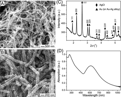 | ||
| Fig. 12 Characterization of the products obtained through galvanic reaction between Ag nanowires and excessive aqueous solution of HAuCl4 at room temperature of 22 °C: (A, B) SEM images with different magnifications; (C) XRD pattern recorded with a synchrotron X-ray with wavelength of 0.107980 Å; (D) UV-visible absorption spectrum of an aqueous dispersion of the resulting nanowires. The absorption spectrum was normalized against the intensity of the peak at 266 nm. | ||
The characterization results of the nanowires shown in Fig. 12A imply that the AgCl nanoparticles and Au nanoparticles in the each nanowire may uniformly distribute rather than phase separation into clusters of nanoparticles made of single components. On the other hand, if Ag nanowires react with FeCl3, nanowires of pure AgCl can be synthesized because the reduced product (FeCl2) of FeCl3 is soluble in water at room temperature. Desired metal nanoparticles can be further deposited on the surfaces of the resulting AgCl nanowires through electroless plating, leading to the formation of AgCl/metal core/shell nanowires. The spatial distribution of AgCl and metal can be well defined in the hybrid nanowires. Fig. 13A sketches the two-step strategy for the synthesis of AgCl/Au core/shell nanowires with the use of Ag nanowires as chemical templates. The nanowires cannot retain the crystallinity and morphology of the original Ag nanowire templates during the reactions highlighted in Fig. 13A, each nanowire is illustrated as a cylinder for simplicity and generality. In the first step, reaction of Ag nanowires with aqueous solution of FeCl3 at room temperature chemically transforms them to polycrystalline AgCl nanowires:
| Ag + FeCl3 → AgCl(precipitate) + FeCl2 | (8) |
![Synthesis and characterization of uniform AgCl nanowires and core/shell nanowires made of AgCl cores decorated with Au nanoparticles. (A) Schematic illustration of chemical conversion of Ag nanowires into AgCl ones and AgCl/Au core/shell ones. The white curves represent grain boundaries, highlighting the polycrystallinity of AgCl nanowires. (B–D) SEM images of (B) Ag nanowires, (C) AgCl nanowires, and (D) core/shell nanowires made of AgCl nanowires coated with Au nanoparticles. (E) Comparison of absorption spectra of the AgCl nanowires with (red curve) and without (black curve) Au nanoparticles. [Adapted with permission from ref. 157, Copyright 2010 American Chemical Society].](/image/article/2010/NR/c0nr00258e/c0nr00258e-f13.gif) | ||
| Fig. 13 Synthesis and characterization of uniform AgCl nanowires and core/shell nanowires made of AgCl cores decorated with Au nanoparticles. (A) Schematic illustration of chemical conversion of Ag nanowires into AgCl ones and AgCl/Au core/shell ones. The white curves represent grain boundaries, highlighting the polycrystallinity of AgCl nanowires. (B–D) SEM images of (B) Ag nanowires, (C) AgCl nanowires, and (D) core/shell nanowires made of AgCl nanowires coated with Au nanoparticles. (E) Comparison of absorption spectra of the AgCl nanowires with (red curve) and without (black curve) Au nanoparticles. [Adapted with permission from ref. 157, Copyright 2010 American Chemical Society]. | ||
The driving force for this reaction relies on the reduced standard reduction potential of Ag couples from 0.80 V (vs. SHE for Ag+/Ag pair) to 0.223 V (vs. SHE for AgCl/Ag pair), which is lower than that (0.771 V vs. SHE) of the Fe3+/Fe2+ pair. Each Ag nanowire serves as a chemical template to guide the resulting AgCl to nucleate and grow into a nanowire during the reaction of eqn (8). Due to large mismatch (35.7%) of lattice constant between AgCl and Ag (5.547 Å vs. 4.0862 Å), the resulting AgCl nanowires usually exhibit polycrystallinity and thicker cross sections. In the second step, addition of precursor containing AuCl4− ions (e.g. NaAuCl4) to the reaction system initiates the redox reaction between AuCl4− and Fe2+ ions (which are generated from reaction of eqn (8)):
| AuCl4− + 3Fe2+ → Au + 3Fe3+ + 4Cl− | (9) |
Fig. 13B–D compare SEM images of the Ag nanowires, AgCl nanowires, and AgCl/Au core/shell hybrid nanowires, clearly showing the increased surface roughness and diameters after conversion of the Ag nanowires into AgCl and AgCl/Au ones. Each polycrystalline AgCl nanowire consists of multiple AgCl particles assembled in one dimension and is composed of essentially pure AgCl, confirmed with compositional analysis. Optical absorption spectrum of an aqueous dispersion of the AgCl nanowires exhibits a peak in the UV region, i.e. at ∼270 nm (black curve in Fig. 13E). After deposition of Au nanoparticles (i.e. the dots with brighter contrast in Fig. 13D), the hybrid core/shell nanowires become even rougher and thicker. Attachment of the Au nanoparticles on the surfaces of the AgCl nanowires increases optical absorption of the hybrid AgCl/Au nanowires in the visible region because of strong SPRs associated with the Au nanoparticles. Fig. 13E compares absorption spectra of the AgCl nanowires before and after decoration with Au nanoparticles, clearly showing the appearance of a new peak centered at 580 nm. The slight increase in intensity of the absorption peak (at ∼270 nm) of AgCl caused by deposition of Au nanoparticles might be ascribed to the coupling of AgCl with plasmonic metal nanoparticles. Similar strategy has recently been employed by Bi and Ye to synthesize Ag/AgCl core/shell nanowires as well as AgCl nanotubes decorated with Pt nanoparticles, which are different from our solid AgCl nanowires.158,159 The structural difference can be attributed to the difference of diameters (40–50 nm in our work shown in Fig. 13vs. ∼100 nm in Bi and Ye's work) of the Ag nanowire templates.
It is well known that AgCl is a good photocatalyst under illumination of UV light (due to its large bandgaps: a direct bandgap of 5.15 eV, or 241 nm, and an indirect bandgap of 3.25 eV, or 382 nm)160 for applications in decomposition of organic pollutants and disinfection of water.161,162 The enhanced absorption of the AgCl/Au core/shell nanowires in the visible region is favorable for them to drive photocatalytic reactions with visible light (or the sunlight).163–166Fig. 14A plots a series of absorption spectra of an aqueous solution of methylene blue (MB) before and after a mixture of AgCl/Au nanowires (as shown in Fig. 13D) and MB molecules is illuminated with a cold white lamp (with emission wavelength in the range of 400–850 nm) for different times. The mixture has to be incubated in the dark for 45 min to reach adsorption/desorption equilibrium of the MB molecules on the nanowire surfaces before it is placed under light, leading to 17.7% of the MB molecules adsorbed to both nanowire surfaces and reactor walls. Under photo-illumination, the absorption of the MB molecules monotonically decreases, indicating the MB molecules are effectively decomposed with assistance of the AgCl/Au nanowires for harvesting the visible light. Degradation kinetics of the MB molecules is monitored by the change of their concentration, which is approximately calculated according to the absorbance at 660 nm (i.e. position of the major peak of the MB molecules). As shown in Fig. 14B, ln(C/C0) and the reaction time (t) exhibits a linear relationship, indicating that the decomposition reaction of MB molecules follows the first-order kinetics:
 | (10) |
![(A) Absorption spectra of the MB molecules recorded at different time since the mixture of AgCl/Au core/shell nanowires and MB molecules was exposed to visible light. (B) Photocatalytic degradation kinetics of the MB molecules for 3 successive reactions with assistance of the same batch of AgCl/Au core/shell nanowires under visible illumination. The spectra in (A) correspond to the first run of reaction. The rate constants, which were calculated according to eqn (10) by linearly fitting the experimental data, are also presented. [Adapted with permission from ref. 157, Copyright 2010 American Chemical Society].](/image/article/2010/NR/c0nr00258e/c0nr00258e-f14.gif) | ||
| Fig. 14 (A) Absorption spectra of the MB molecules recorded at different time since the mixture of AgCl/Au core/shell nanowires and MB molecules was exposed to visible light. (B) Photocatalytic degradation kinetics of the MB molecules for 3 successive reactions with assistance of the same batch of AgCl/Au core/shell nanowires under visible illumination. The spectra in (A) correspond to the first run of reaction. The rate constants, which were calculated according to eqn (10) by linearly fitting the experimental data, are also presented. [Adapted with permission from ref. 157, Copyright 2010 American Chemical Society]. | ||
In addition to silver halides, nanowires made of silver chalcogenides, such as Ag2S, Ag2Se have also been synthesized through the reaction between Ag nanowires and aqueous solutions containing S2− or Se2− ions in the presence of oxygen dissolved in the reaction solutions.79,167 Once silver chalcogenide nanowires are synthesized, cationic exchange of Ag+ with other ions, such as Cd2+, Pb2+etc. can transform them into different chalcogenide nanowires.168,169 As a result, nanowires made of large amount of chalcogenides can be synthesized by templating against Ag nanowires through chemical transformation and the resulting semiconductor nanowires may find applications in electronics and energy conversion including photovoltaics and photocatalysis.
6. Conclusion and remarks
Silver nanowires as well as other 1D nanostructures derived from Ag nanowires are discussed in this article with emphasis on: i) high-yield synthesis of Ag nanowires through polyol process; ii) synthesis of metal/dielectric core/shell nanowires (or coaxial nanocables) with the use of Ag nanowires as physical templates; iii) synthesis of metal nanotubes and semiconductor nanowires as well as semiconductor/metal hybrid nanowires with the use of Ag nanowires as chemical templates. The nanostructures derived from Ag nanowires are difficult (or impossible) to synthesize through other approaches and exhibit unique properties in terms of electrical, optical, electronic, and catalytic characteristics, which may lead to potential applications in varying areas, such as nanoelectronics, nanophotonics, photocatalysis, photovoltaics, and medicine. Due to the 1D anisotropic geometry of nanowires, they may perform better than their counterparts with isotropic morphologies. In combination with hollow interiors associated with nanotubes, the performance in some applications can be even further improved. For example, using Ag nanowires as fillers of polymeric conductive composites can significantly decreases the volume ratio in comparison with spherical Ag particles. The amount of metal usage can be further decreased with the use of Au-Ag alloy nanotubes as the conductive fillers. Another potential example is the use of Ag nanowires and Au-Ag alloy nanotubes as plasmonic waveguides for propagating energy within the sub-wavelength confinement. As discussed in Introduction, the chemically synthesized Ag nanowires have been demonstrated as one of the best building blocks serving as plasmonic waveguides in varying nanophotonic elements with different functionalities. However, the inherent absorption losses of metal place a hard limit on propagation lengths in the nanowires. On the other hand, plasmon propagation in hollow metal nanotubes (such as Au-Ag alloy nanotubes shown in Fig. 6C) may behave differently from the solid nanowires. When a metal nanotube that consist of a thin metal shell enclosing a hollow core is excited with external photons, plasmons on the outer surface of the shell couples to plasmons on the inner surface, splitting the dispersion relation into two separate modes, or branches.170 These modes are analogous to the symmetric and antisymmetric surface-plasmon modes that propagate along thin metal films. The lower-energy, antisymmetric mode, in particular, is known as a long-range surface plasmon, because it can have very long propagation distances.170,171 Similarly, the lower-energy mode in hollow metal nanotubes should exhibit dramatically lower losses than is seen in solid metal nanowires, making them attractive for the nanoscale propagation of optical energy. As a result, metal nanotubes derived from the Ag nanowire templates might be a next generation nanomaterial for supporting long-range SPP propagation. These two examples shed light on how the transformation of Ag nanowires into other 1D nanostructures impacts their properties, functionalities, as well as their performance in applications, which represent the future research directions on Ag nanowires as well as their derivatives.Acknowledgements
Use of the Center for Nanoscale Materials, the Electron Microscopy Center for Materials Research, and the Advanced Photon Source (APS) at Argonne was supported by the U. S. Department of Energy, Office of Science, Office of Basic Energy Sciences, under Contract No. DE-AC02-06CH11357. Help from Dr Yang Ren for XRD measurements on beamline 11-ID-C of APS is greatly appreciated.References
- C. Ducamp-Sanguesa, R. Herrera-Urbina and M. Figlarz, J. Solid State Chem., 1992, 100, 272 CrossRef.
- V. M. Cepak and C. R. Martin, J. Phys. Chem. B, 1998, 102, 9985 CrossRef CAS.
- D. D. Lu, Y. G. Li and C. P. Wong, J. Adhes. Sci. Technol., 2008, 22, 815 CrossRef CAS.
- H. Wu, X. Wu, J. Liu, G. Zhang, Y. Wang, Y. Zeng and J. Jing, J. Compos. Mater., 2006, 40, 1961 CrossRef CAS.
- A. Munari, J. Xu, E. Dalton, A. Mathewson, and K. M. Razeeb, 2009 IEEE 59th Electronic Components and Technology Conference 59th Electronic Components and Technology Conference, San Diego, CA, 2009, p. 448 Search PubMed.
- G. A. Gelves, U. Sundararaj and J. A. Haber, Macromol. Rapid Commun., 2005, 26, 1677 CrossRef CAS.
- I. Balberg and N. Binenbaum, Phys. Rev. Lett., 1984, 52, 1465 CrossRef.
- A. Kumar and C. Zhou, ACS Nano, 2010, 4, 11 CrossRef CAS.
- J.-Y. Lee, S. T. Connor, Y. Cui and P. Peumans, Nano Lett., 2008, 8, 689 CrossRef CAS.
- S. De, T. M. Higgins, P. E. Lyons, E. M. Doherty, P. N. Nirmalraj, W. J. Blau, J. J. Boland and J. N. Coleman, ACS Nano, 2009, 3, 1767 CrossRef CAS.
- J.-Y. Lee, S. T. Connor, Y. Cui and P. Peumans, Nano Lett., 2010, 10, 1276 CrossRef CAS.
- K. L. Kelly, E. Coronado, L. L. Zhao and G. C. Schatz, J. Phys. Chem. B, 2003, 107, 668 CrossRef CAS.
- C. Burda, X. Chen, R. Narayanan and M. A. El-Sayed, Chem. Rev., 2005, 105, 1025 CrossRef CAS.
- B. J. Wiley, S. H. Im, Z.-Y. Li, J. McLellan, A. Siekkinen and Y. Xia, J. Phys. Chem. B, 2006, 110, 15666 CrossRef CAS.
- M. E. Stewart, C. R. Anderton, L. B. Thompson, J. Maria, S. K. Gray, J. A. Rogers and R. G. Nuzzo, Chem. Rev., 2008, 108, 494 CrossRef CAS.
- A. R. Tao, S. Habas and P. Yang, Small, 2008, 4, 310 CrossRef CAS.
- T. K. Sau, A. L. Rogach, F. Jackel, T. A. Klar and J. Feldmann, Adv. Mater., 2010, 22, 1805 CrossRef CAS.
- H. Ko, S. Singamaneni and V. V. Tsukruk, Small, 2008, 4, 1576 CrossRef CAS.
- M. Moskovits, J. Raman Spectrosc., 2005, 36, 485 CrossRef CAS.
- S.-H. Guo, D. G. Britti, J. J. Heetderks, H.-C. Kan and R. J. Phaneuf, Nano Lett., 2009, 9, 2666 CrossRef CAS.
- W. Feng, L.-D. Sun and C.-H. Yan, Chem. Commun., 2009,(29), 4393 RSC.
- P. Mohanty, I. Yoon, T. Kang, K. Seo, S. K. Varadwaj, W. Choi, Q.-H. Park, J. P. Ahn, Y. D. Suh, H. Ihee and B. Kim, J. Am. Chem. Soc., 2007, 129, 9576 CrossRef CAS.
- C. Du, Y. You, X. Zhang, K. Johnson and Z. Shen, Plasmonics, 2009, 4, 217 CrossRef CAS.
- P. H. C. Camargo, C. M. Cobley, M. Rycenga and Y. Xia, Nanotechnology, 2009, 20, 434020 CrossRef.
- R. F. Aroca, P. J. G. Goulet, D. S. dos Santos, Jr., R. A. Alvarez-Puebla and O. N. Oliveira, Jr., Anal. Chem., 2005, 77, 378 CrossRef CAS.
- A. Tao, F. Kim, C. Hess, J. Goldberger, R. He, Y. Sun, Y. Xia and P. Yang, Nano Lett., 2003, 3, 1229 CrossRef CAS.
- A. R. Tao and P. Yang, J. Phys. Chem. B, 2005, 109, 15687 CrossRef CAS.
- S. J. Lee, A. R. Morrill and M. Moskovits, J. Am. Chem. Soc., 2006, 128, 2200 CrossRef CAS.
- D. H. Jeong, Y. X. Zhang and M. Moskovits, J. Phys. Chem. B, 2004, 108, 12724 CrossRef CAS.
- R. Gunawidjaja, S. Peleshanko, H. Ko and V. V. Tsukruk, Adv. Mater., 2008, 20, 1544 CrossRef CAS.
- S. J. Lee, J. M. Baik and M. Moskovits, Nano Lett., 2008, 8, 3244 CrossRef CAS.
- R. M. Dickson and L. A. Lyon, J. Phys. Chem. B, 2000, 104, 6095 CrossRef CAS.
- A. Graff, D. Wagner, H. Ditlbacher and U. Kreibig, Eur. Phys. J. D, 2005, 34, 263 CrossRef CAS.
- A. W. Sanders, D. A. Routenberg, B. J. Wiley, Y. Xia, E. R. Dufresne and M. A. Reed, Nano Lett., 2006, 6, 1822 CrossRef CAS.
- C.-H. Dong, X.-F. Ren, R. Yang, J. Y. Duan, J.-G. Guan, G.-C. Guo and G.-P. Guo, Appl. Phys. Lett., 2009, 95, 221109 CrossRef.
- H. Wei, D. Ratchford, X. Li, H. Xu and C.-K. Shih, Nano Lett., 2009, 9, 4168 CrossRef CAS.
- A. V. Akimov, A. Mukherjee, C. L. Yu, D. E. Chang, A. S. Zibrov, P. R. Hemmer, H. Park and M. D. Lukin, Nature, 2007, 450, 402 CrossRef CAS.
- X. Guo, M. Qiu, J. Bao, B. J. Wiley, Q. Yang, X. Zhang, Y. Ma, H. Yu and L. Tong, Nano Lett., 2009, 9, 4515 CrossRef CAS.
- R. Yan, P. Pausauskie, J. Huang and P. Yang, Proc. Natl. Acad. Sci. U. S. A., 2009, 106, 21045 CrossRef CAS.
- A. L. Pyayt, B. J. Wiley, Y. Xia, A. Chen and L. Dalton, Nat. Nanotechnol., 2008, 3, 660 CrossRef CAS.
- J. A. Hutchison, S. P. Centeno, H. Odaka, H. Fukumura, J. Hofkens and H. Uji-i, Nano Lett., 2009, 9, 995 CrossRef CAS.
- Y. Fang, H. Wei, F. Hao, P. Nordlander and H. Xu, Nano Lett., 2009, 9, 2049 CrossRef CAS.
- X. Liu, J. Luo and J. Zhu, Nano Lett., 2006, 6, 408 CrossRef CAS.
- A. Singh and A. Ghosh, J. Phys. Chem. C, 2008, 112, 3460 CrossRef CAS.
- B. Wang, G. T. Fei, Y. Zhou, B. Wu, X. Zhu and L. Zhang, Cryst. Growth Des., 2008, 8, 3073 CrossRef CAS.
- Y. Xia, P. Yang, Y. Sun, Y. Wu, B. Mayers, B. Gates, Y. Yin, F. Kim and H. Yan, Adv. Mater., 2003, 15, 353 CrossRef CAS.
- R. M. Penner, J. Phys. Chem. B, 2002, 106, 3339 CrossRef CAS.
- H. H. Song, K. M. Jones and A. A. Baski, J. Vac. Sci. Technol., A, 1999, 17, 1696 CrossRef CAS.
- M. H. Huang, A. Choudrey and P. Yang, Chem. Commun., 2000,(12), 1063 RSC.
- S. Bhattacharyya, S. K. Saha and D. Chakravorty, Appl. Phys. Lett., 2000, 77, 3770 CrossRef CAS.
- Y.-J. Han, J. M. Kim and G. D. Stucky, Chem. Mater., 2000, 12, 2068 CrossRef CAS.
- B. H. Hong, S. C. Bae, C.-W. Lee, S. Jeong and K. S. Kim, Science, 2001, 294, 348 CrossRef CAS.
- J. Chai, D. Wang, X. Fan and J. Buriak, Nat. Nanotechnol., 2007, 2, 500 CrossRef.
- D. Zhang, L. Qi, J. Ma and H. Cheng, Chem. Mater., 2001, 13, 2753 CrossRef CAS.
- E. Braun, Y. Eichen, U. Sivan and G. Ben-Yoseph, Nature, 1998, 391, 775 CrossRef CAS.
- H. Yan, S. H. Park, G. Finkelstein, J. H. Reif and T. H. LaBean, Science, 2003, 301, 1882 CrossRef CAS.
- H. A. Becerril, R. M. Stoltenberg, C. F. Monson and A. T. Woolley, J. Mater. Chem., 2004, 14, 611 RSC.
- G. Wei, H. Zhou, Z. Liu, Y. Song, L. Wang, L. Sun and Z. Li, J. Phys. Chem. B, 2005, 109, 8738 CrossRef CAS.
- M. Reches and E. Gazit, Science, 2003, 300, 625 CrossRef CAS.
- S. Behrens, J. Wu, W. Habicht and E. Unger, Chem. Mater., 2004, 16, 3085 CrossRef CAS.
- K. T. Nam, Y. J. Lee, E. M. Krauland, S. T. Kottmann and A. M. Belcher, ACS Nano, 2008, 2, 1480 CrossRef CAS.
- J. Sloan, D. M. Wright, H.-G. Woo, S. Bailey, G. Brown, A. P. E. York, K. S. Coleman, J. L. Hutchison and M. L. H. Green, Chem. Commun., 1999,(8), 699 RSC.
- Y. Xia, Y. Xiong, B. Lim and S. E. Skrabalak, Angew. Chem., Int. Ed., 2009, 48, 60 CrossRef CAS.
- J. Chen, B. J. Wiley and Y. Xia, Langmuir, 2007, 23 Search PubMed.
- N. R. Jana, L. Gearheart and C. J. Murphy, Chem. Commun., 2001,(7), 617 RSC.
- C. J. Murphy and N. R. Jana, Adv. Mater., 2002, 14, 80 CrossRef CAS.
- C. J. Murphy, A. M. Gole, S. E. Hunyadi and C. J. Orendorff, Inorg. Chem., 2006, 45, 7544 CrossRef CAS.
- M. Lucas, A. M. Leach, M. T. McDowell, S. E. Hunyadi, K. Gall, C. J. Murphy and E. Riedo, Phys. Rev. B: Condens. Matter Mater. Phys., 2008, 77, 245420 CrossRef.
- C. Ni, P. A. Hassan and E. W. Kaler, Langmuir, 2005, 21, 3334 CrossRef CAS.
- S.-H. Zhang, Z.-Y. Jiang, Z.-X. Xie, X. Xu, R.-B. Huang and L.-S. Zheng, J. Phys. Chem. B, 2005, 109, 9416 CrossRef CAS.
- S. H. Kim, B. S. Choi, K. Kang, Y.-S. Choi and S. I. Yang, J. Alloys Compd., 2007, 433, 261 CrossRef CAS.
- X. Zheng, L. Zhu, A. Yan, X. Wang and Y. Xie, J. Colloid Interface Sci., 2003, 268, 357 CrossRef CAS.
- G. Zhou, M. Lu, Z. Yang, H. Zhang, Y. Zhou, S. Wang, S. Wang and A. Zhang, J. Cryst. Growth, 2006, 289, 255 CrossRef CAS.
- B. Pietrobon and V. Kitaev, Chem. Mater., 2008, 20, 5186 CrossRef CAS.
- X. Zheng, X. ZHao, D. Guo, B. Tang, S. Xu, B. Zhao and W. Xu, Langmuir, 2009, 25, 3802 CrossRef CAS.
- K. G. Stamplecoskie and J. C. Scaiano, J. Am. Chem. Soc., 2010, 132, 1825 CrossRef CAS.
- D. Seo, C. I. Yoo, I. S. Chung, S. M. Park, S. Ryu and H. Song, J. Phys. Chem. C, 2008, 112, 2469 CrossRef CAS.
- B. Pietrobon, M. McEachran and V. Kitaev, ACS Nano, 2009, 3, 21 CrossRef CAS.
- D. Seo, C. I. Yoo, J. Jung and H. Song, J. Am. Chem. Soc., 2008, 130, 2940 CrossRef CAS.
- Y. Sun, B. Mayers, T. Herricks and Y. Xia, Nano Lett., 2003, 3, 955 CrossRef CAS.
- Y. Sun, B. Gates, B. Mayers and Y. Xia, Nano Lett., 2002, 2, 165 CrossRef CAS.
- Y. Sun and Y. Xia, Adv. Mater., 2002, 14, 833 CrossRef CAS.
- Y. Sun, Y. Yin, B. T. Mayers, T. Herricks and Y. Xia, Chem. Mater., 2002, 14, 4736 CrossRef CAS.
- C. J. Johnson, E. Dujardin, S. A. Davis, C. J. Murphy and S. Mann, J. Mater. Chem., 2002, 12, 1765 RSC.
- I. Lisiecki, A. Filankembo, H. Sack-Kongehl, K. Weiss, M.-P. Pileni and J. Urban, Phys. Rev. B: Condens. Matter Mater. Phys., 2000, 61, 4968 CrossRef.
- P.-Y. Silvert, R. Herrera-Urbina and K. Tekaia-Elhsissen, J. Mater. Chem., 1997, 7, 293 RSC.
- Y. Gao, P. Jiang, D. F. Liu, H. J. Yuan, X. Q. Yan, Z. P. Zhou, J. X. Wang, L. Song, L. F. Liu, W. Y. Zhou, G. Wang, C. Y. Wang, S. S. Xie, J. M. Zhang and D. Y. Shen, J. Phys. Chem. B, 2004, 108, 12877 CrossRef CAS.
- Y. Gao, P. Jiang, L. Song, L. Liu, X. Yan, Z. Zhou, D. Liu, J. Wang, H. Yuan, Z. Zhang, X. Zhao, X. Dou, W. Y. Zhou, G. Wang and S. Xie, J. Phys. D: Appl. Phys., 2005, 38, 1061 CrossRef CAS.
- L.-B. Luo, S.-H. Yu, H.-S. Qian and T. Zhou, J. Am. Chem. Soc., 2005, 127, 2822 CrossRef CAS.
- T. Y. Kim, W. J. Kim, S. H. Hong, J. E. Kim and K. S. Suh, Angew. Chem., Int. Ed., 2009, 48, 3806 CrossRef CAS.
- B. Wiley, T. Herricks, Y. Sun and Y. Xia, Nano Lett., 2004, 4, 1733 CrossRef CAS.
- B. Wiley, Y. Sun and Y. Xia, Langmuir, 2005, 21, 8077 CrossRef CAS.
- Q. Zhang, C. Cobley, L. Au, M. Mckiernan, A. Schwartz, L.-P. Wen, J. Chen and Y. Xia, ACS Appl. Mater. Interfaces, 2009, 1, 2044 Search PubMed.
- K. E. Korte, S. E. Skrabalak and Y. Xia, J. Mater. Chem., 2008, 18, 437 RSC.
- A. R. Siekkinen, J. M. McLellan, J. Chen and Y. Xia, Chem. Phys. Lett., 2006, 432, 491 CrossRef CAS.
- S. H. Im, Y. T. Lee, B. Wiley and Y. Xia, Angew. Chem., Int. Ed., 2005, 44, 2154 CrossRef.
- T. Herricks, J. Chen and Y. Xia, Nano Lett., 2004, 4, 2367 CrossRef CAS.
- J. Chen, T. Herricks, M. Geissler and Y. Xia, J. Am. Chem. Soc., 2004, 126, 10854 CrossRef CAS.
- S. Guo, S. Dong and E. Wang, Cryst. Growth Des., 2009, 9, 372 CrossRef CAS.
- M. Tsuji, K. Matsumoto, P. Jiang, R. Matsuo, X.-L. Tang, K. Sozana and N. Kamarudin, Colloids Surf., A, 2008, 316, 266 CrossRef CAS.
- X. Tang, M. Tsuji, M. Nishio and P. Jiang, Bull. Chem. Soc. Jpn., 2009, 82, 1304 CrossRef CAS.
- J. Jiu, K. Murai, D. Kim, K. S. Kim and K. Suganuma, Mater. Chem. Phys., 2009, 114, 333 CrossRef CAS.
- Y. Bi, H. Hu and G. Lu, Chem. Commun., 2010, 46, 598 RSC.
- K. K. Caswell, C. M. Bender and C. J. Murphy, Nano Lett., 2003, 3, 667 CrossRef CAS.
- Y. Yin, Y. Lu, Y. Sun and Y. Xia, Nano Lett., 2002, 2, 427 CrossRef CAS.
- S. E. Hunyadi and C. J. Murphy, J. Phys. Chem. B, 2006, 110, 7226 CrossRef CAS.
- J. A. Sioss, R. L. Stoermer, M. Y. Sha and K.C.D., Langmuir, 2007, 23, 11334 CrossRef CAS.
- C. Gutierrez-Wing, R.R. Perez-Hernandez, M. Mondragon-Galicia, G. Villa-Sanchez, M. E. Fernandez-Garcia, J. Arenas-Alatorre and D. Mendoza-Anaya, Solid State Sci., 2009, 11, 1722 CrossRef CAS.
- Y.-G. Guo, L.-J. Wan and C.-L. Bai, J. Phys. Chem. B, 2003, 107, 5441 CrossRef CAS.
- S. O. Obare, N. R. Jana and C. J. Murphy, Nano Lett., 2001, 1, 601 CrossRef CAS.
- L.-B. Luo, S.-H. Yu, H.-S. Qian and J.-Y. Gong, Chem.–Eur. J., 2006, 12, 3320 CrossRef CAS.
- X. Duan and Y. Huang, in 'Chemically synthesized semiconductor nanowires for high-performance electronics and optoelectronics', ed. Y. Sun and J. A. Rogers, Boston, 2010 Search PubMed.
- C. M. Lieber, Sci. Am., 2001, 285, 58 CrossRef CAS.
- J. Xiang, W. Lu, Y. Hu, Y. Wu, H. Yan and C. M. Lieber, Nature, 2006, 441, 489 CrossRef CAS.
- X. Duan, Y. Huang, R. Agarwal and C. M. Lieber, Nature, 2003, 421, 241 CrossRef CAS.
- Q. Zhang, W. Wang, J. Goebl and Y. Yin, Nano Today, 2009, 4, 494 CrossRef CAS.
- T. Zhang, Q. Zhang, J. Ge, J. Goebl, M. Sun, Y. Yan, Y.-S. Liu, C.-L. Chang, J. Guo and Y. Yin, J. Phys. Chem. C, 2009, 113, 3168 CrossRef CAS.
- Q. Zhang, T. Zhang, J. Ge and Y. Yin, Nano Lett., 2008, 8, 2867 CrossRef CAS.
- J. Ge, Q. Zhang, T. Zhang and Y. Yin, Angew. Chem., Int. Ed., 2008, 47, 8924 CrossRef CAS.
- Y. Sun and Y. Xia, J. Am. Chem. Soc., 2004, 126, 3892 CrossRef CAS.
- Z. L. Wang, T. S. Ahmad and M. A. El-Sayed, Surf. Sci., 1997, 380, 302 CrossRef CAS.
- D. Seo and H. Song, J. Am. Chem. Soc., 2009, 131, 18210 CrossRef CAS.
- T. Shibata, B. A. Bunker, Z. Zhang, D. Meisel, C. F. Vardeman, II and J. D. Gezelter, J. Am. Chem. Soc., 2002, 124, 11989 CrossRef CAS.
- H. Shi, L. Zhang and W. Cai, J. Appl. Phys., 2000, 87, 1572 CrossRef CAS.
- J. Erlebacher, M. J. Aziz, A. Karma, N. Dimitrov and K. Sieradzki, Nature, 2001, 410, 450 CrossRef CAS.
- Y. Ding, Y.-J. Kim and J. Erlebacher, Adv. Mater., 2004, 16, 1897 CrossRef CAS.
- K. Sieradzki, J. Electrochem. Soc., 1993, 140, 2868 CrossRef CAS.
- A. R. Roosen and W. C. Carter, Phys. A, 1998, 261, 232 CrossRef.
- I. Lampre, P. Pernot and M. Mostafavi, J. Phys. Chem. B, 2000, 104, 6233 CrossRef CAS.
- J. Chen, F. Saeki, B. J. Wiley, H. Cang, M. J. Cobb, Z.-Y. Li, L. Au, H. Zhang, M. B. Kimmey, X. Li and Y. Xia, Nano Lett., 2005, 5, 473 CrossRef CAS.
- R. Allabashi, W. Stach, A. de la Escosura-Muniz, L. Liste-Calleja and A. Merkoci, J. Nanopart. Res., 2009, 11, 2003 CrossRef CAS.
- S. E. Skrabalak, J. Chen, Y. Sun, X. Lu, L. Au, C. M. Cobley and Y. Xia, Acc. Chem. Res., 2008, 41, 1587 CrossRef CAS.
- C. J. Murphy, A. M. Gole, J. W. Stone, P. N. Sisco, A. M. Alkilany, E. C. Goldsmith and S. C. Baxter, Acc. Chem. Res., 2008, 41, 1721 CrossRef CAS.
- X. Huang, S. Neretina and M. A. El-Sayed, Adv. Mater., 2009, 21, 4880 CrossRef CAS.
- P. K. Jain, X. Huang, I. H. El-Sayed and M. A. El-Sayed, Acc. Chem. Res., 2008, 41, 1578 CrossRef CAS.
- J. Chen, D. Wang, J. Xi, L. Au, A. Siekkinen, A. Warsen, Z.-Y. Li, H. Zhang, Y. Xia and X. Li, Nano Lett., 2007, 7, 1318 CrossRef CAS.
- J. R. Cole, N. A. Mirin, M. W. Knight, G. P. Goodrich and N. J. Halas, J. Phys. Chem. C, 2009, 113, 12090 CrossRef CAS.
- S. Lal, S. E. Clare and N. J. Halas, Acc. Chem. Res., 2008, 41, 1842 CrossRef CAS.
- M. S. Yavuz, Y. Cheng, J. Chen, C. M. Cobley, Q. Zhang, M. Rycenga, J. Xie, C. Kim, K. H. Song, A. G. Schwartz, L. V. Wang and Y. Xia, Nat. Mater., 2009, 8, 935 CrossRef CAS.
- A. Barhoumi, R. Huschka, R. Bardhan, M. W. Knight and N. J. Halas, Chem. Phys. Lett., 2009, 482, 171 CrossRef CAS.
- Y. Sun, B. Mayers and Y. Xia, Adv. Mater., 2003, 15, 641 CrossRef CAS.
- J. Greeley, I. E. L. Stephens, A. S. Bondarenko, T. P. Johansson, H. A. Hansen, T. F. Jaramillo, J. Rossmeisl, I. Chorkendorff and J. K. Norskov, Nat. Chem., 2009, 1 Search PubMed.
- V. R. Stamenkovic, B. Fowler, B. S. Mun, G. Wang, P. N. Ross, C. A. Lucas and N. M. Markovic, Science, 2007, 315, 493 CrossRef CAS.
- N. Tian, Z.-Y. Zhou, S.-G. Sun, Y. Ding and Z. L. Wang, Science, 2007, 316, 732 CrossRef CAS.
- B. Lim, M. Jiang, P. H. C. Camargo, E. C. Cho, J. Tao, X. Lu, Y. Zhu and Y. Xia, Science, 2009, 324, 1302 CrossRef CAS.
- S. H. Joo, J. Y. Park, C.-K. Tsung, Y. Yamada, P. Yang and G. A. Somorjai, Nat. Mater., 2009, 8, 126 CrossRef CAS.
- S. Vajda, M. J. Pellin, J. P. Greeley, C. L. Marshall, L. A. Curtiss, G. A. Ballentine, J. W. Elam, S. Catillon-Mucherie, P. C. Redfern, F. Mehmood and P. Zapol, Nat. Mater., 2009, 8, 213 CrossRef.
- H. M. Chen, R.-S. Liu, M.-Y. Lo, S.-C. Chang, L.-D. Tsai, Y.-M. Peng and J.-F. Lee, J. Phys. Chem. C, 2008, 112, 7522 CrossRef CAS.
- Y. Sun, Z. Tao, J. Chen, T. Herricks and Y. Xia, J. Am. Chem. Soc., 2004, 126, 5940 CrossRef CAS.
- O. M. Lovvik and R. A. Olsen, J. Alloys Compd., 2002, 330–332, 332 CrossRef CAS.
- M. Lahav, T. Sehayek, A. Vaskevich and I. Rubinstein, Angew. Chem., Int. Ed., 2003, 42, 5576 CrossRef CAS.
- Y. Sun and Y. Xia, Adv. Mater., 2004, 16, 264 CrossRef CAS.
- Y. Sun, B. Wiley, Z.-Y. Li and Y. Xia, J. Am. Chem. Soc., 2004, 126, 9399 CrossRef CAS.
- S. E. Hunyadi and C. J. Murphy, J. Cluster Sci., 2009, 20, 319 CrossRef CAS.
- L. Au, X. Lu and Y. Xia, Adv. Mater., 2008, 20, 2517 CrossRef CAS.
- Y. Sun and C. Lei, Angew. Chem., Int. Ed., 2009, 48, 6824 CrossRef CAS.
- Y. Sun, J. Phys. Chem. C, 2010, 114, 2127 CrossRef CAS.
- Y. Bi and J. Ye, Chem. Commun., 2009, 6551 RSC.
- Y. Bi and J. Ye, Chem. Commun., 2010, 46, 1532 RSC.
- J. S.-Y. Wang, M. Schluter and M. L. Cohen, Phys. Status Solidi B, 1976, 77, 295.
- S. Malato, J. Blanco, D. C. Alarcon, M. I. Maldonado, P. Fernandez-Ibanez and W. Gernjak, Catal. Today, 2007, 122, 137 CrossRef CAS.
- M. R. Hoffmann, S. T. Martin, W. Choi and D. W. Bahnemann, Chem. Rev., 1995, 95, 69 CrossRef CAS.
- P. Wang, B. Huang, X. Qin, X. Zhang, Y. Dai, J. Wei and M.-H. Whangbo, Angew. Chem., Int. Ed., 2008, 47, 7931 CrossRef CAS.
- P. Wang, B. Huang, Z. Lou, X. Zhang, X. Qin, Y. Dai, Z. Zheng and X. Wang, Chem.–Eur. J., 2010, 16, 538 CrossRef CAS.
- J. Yu, G. Dai and B. Huang, J. Phys. Chem. C, 2009, 113, 16394 CrossRef CAS.
- M. Choi, K.-H. Shin and J. Jang, J. Colloid Interface Sci., 2010, 341, 83 CrossRef CAS.
- M. Liu and P. Guyot-Sionnest, J. Mater. Chem., 2006, 16, 3942 RSC.
- D. H. Son, S. M. Hughes, Y. Yin and A. P. Alivisatos, Science, 2004, 306, 1009 CrossRef CAS.
- J. Zhang, Y. Tang, K. Lee and M. Ouyang, Science, 2010, 327, 1634 CrossRef CAS.
- U. Schroter and A. Dereux, Phys. Rev. B: Condens. Matter Mater. Phys., 2001, 64, 125420 CrossRef.
- D. Sarid, Phys. Rev. Lett., 1981, 47, 1927 CrossRef CAS.
| This journal is © The Royal Society of Chemistry 2010 |