DOI:
10.1039/C0NR00111B
(Feature Article)
Nanoscale, 2010,
2, 1611-1625
Received
11th February 2010
, Accepted 6th April 2010
First published on
14th June 2010
Abstract
Among the carbon allotropes newly discovered during the last few decades, carbon nanotubes (CNTs) have attracted enormous attention due to their structural and electronic properties with strong one dimensional character. The physical and chemical features of such systems are intrinsically rich and complex, and can only be probed by using multiple experimental and theoretical techniques. In this feature, we focus on the structural and electronic properties of CNTs that can be accessed by using transmission electron energy loss spectroscopies. The latter are complementary to optical and X-ray absorption techniques, yet allow to obtain the electronic structure with nanoscale spatial resolution. An improved understanding of the structure-electronic properties relationship of these unique 1D systems would represent a fundamental advance, and holds the promise of using CNTs in future applications.
| Paola Castrucci received a fellowship to work at the Italian National Council of Research (CNR) in 1990. In 1992 she became researcher at University of Camerino. Since 2003 she has been researcher at Department of Physics of the Roma Tor Vergata University. Her research activity mainly deals with surfaces, interfaces and nanostructures structural and electronic properties study through electron and X-ray spectroscopy, scanning tunnelling microscopy and transmission electron microscopy. Recently her research interests include photovoltaic and optoelectronic properties. She has published over 75 peer reviewed papers. |
 Manuela Scarselli | Manuela Scarselli is Assistant Professor in solid state physics at the Physics Department of the University of Rome ‘Tor Vergata’ since 2001. Her experimental activity is carried out in Rome where Scanning Tunnelling Microscopy, Atomic Force Microscopy, reflection energy loss and X-ray spectroscopy are available. Her current interests are the following: 1) synthesis, characterization, decoration of carbon nanotubes and their application in photo electrochemical solar cells, 2) growth and optical characterization of Ge dots on SiO2, 3) self-assembly of organic molecules on metallic surfaces. She has published more than 50 peer-reviewed journal papers and participates to international congress and meetings. |
 Maurizio De Crescenzi | Maurizio De Crescenzi is full professor of Structure of Matter at Roma Tor Vergata University and leads the nanostructures group in the Department of Physics. His expertise in Surface Science using Electron Energy Loss, XPS, STM is internationally recognized. He developed Extended Energy Loss Fine Structure, an electron spectroscopy technique as a local surface structural tool. His main fields of investigation are: growth of nanostructures of Ge/Si and Fe/Cu/Si ultrathin films by MBE, synthesis of silicon carbide nanostructures and carbon nanotubes, photovoltaic and optoelectronic investigation of carbon nanotubes. He has organized several International conferences on nanostructures, published about 230 papers and a book on electron spectroscopy. |
 My Ali El Khakani | Professor My Ali El Khakani leads the NanoMat group at Institut National de la Recherche Scientifique (http://www.emt.inrs.ca). He is an internationally recognized expert in laser/plasma based synthesis, nanoassembly and characterization of nanostructured materials (CNTs, NPs etc.) and their application in advanced devices. He has published more than 110 refereed publications in prestigious journals and holds 5 patents. He has been appointed as a scientific expert for various public/private funding agencies, steering committees and scientific committees of international conferences. He has also served on the editorial board of sensors letters and has been acting as a regular reviewer for more than 20 journals. |
 Federico Rosei | Professor Federico Rosei holds the Canada Research Chair in Nanostructured Organic and Inorganic Materials at Institut National de la Recherche Scientifique (INRS-Energie, Materiaux et Telecommunications, Varennes, Qc, Canada). He has research focuses on the fabrication, processing and characterization of inorganic, organic and biocompatible nanomaterials. He has published over 100 articles in prestigious international journals (including Science, Nature Chemistry, Nature Nanotechnology, etc.), has been invited to speak at over 100 international conferences and has given over 120 seminars and colloquia in 33 countries on all inhabited continents. His publications have been cited over 1500 times and his H index is 21. |
1. Introduction
Until the 1980s, the only stable forms of aggregation of carbon into ordered structures were graphite (the most common) and diamond. These two very distinct crystallographic structures are well known for their different properties. As a salient example, graphite is a layered material and behaves as a semi-metal, whereas diamond is the hardest material known so far and is electrically insulating. In 1985, the discovery of fullerenes (so-called buckyballs, i.e. molecules composed of at least 60 carbon atoms arranged in a “soccer ball”-like structure) by Curl, Kroto and Smalley1 marked the beginning of a new era for carbon allotropes. These allotropes can now be divided into three broad categories, namely zero dimensional systems such as fullerenes (C60, C70, C84, etc.), one dimensional systems such as nanotubes (single wall or multi wall)2 and two dimensional systems commonly referred to as graphene (i.e. a single sheet or plane of graphite). While one dimensional carbon nanostructures were first observed in 1976,3 hollow structures named “carbon nanotubes” (CNTs) were met with great interest following the work of Ijima in the early 1990s.4 The fact that low dimensional systems may exhibit radically different (or even unexpected) physical and chemical properties with respect to their bulk counterparts has in fact prompted an explosive growth in the field of nanostructured materials mainly since the mid-1990s. In particular, CNTs have been studied broadly, due to their unique combination of remarkable chemical, optical, electrical and mechanical properties.5 Their unusual ability to transport charge carriers with high mobility has motivated a huge volume of research on their use as active materials in nanoelectronic devices.6–10
The peculiar properties of CNTs and their potential applications propelled the overwhelming scientific effort in their growth, characterization and functionalization. On the fundamental side, this has also fostered investigations to uncover the origin of their unusual behavior. The development of progressively more powerful nanoscale characterization tools allowed to establish correlations between the CNTs nanostructure and the number of defects in the CNTs network, as well as with their physical and chemical properties.
From a structural point of view, CNTs can be divided into two categories, namely single wall carbon nanotubes (SWCNTs) and multiwall carbon nanotubes (MWCNTs). The former consist in a graphene sheet rolled up into a tube. The latter is formed by several SWCNTs concentrically nested into each other. In the SWCNT case, the circumferential lattice vector of graphene, (i.e. the chiral vector), characterized by the (n,m) indices, fully determines the structure of a SWCNT in terms of wrapping angle and diameter. Fig. 1 displays examples of armchair (n,n), zigzag (n,0) and chiral (n,m) SWCNTs. In the tight binding approximation, the application of the periodic boundary conditions to the graphene lattice allows only a discrete number of momenta along the circumference.11,12 As a consequence, the SWCNTs electronic density of states (DOS) exhibits van Hove singularities (which are typical of one-dimensional systems with (E0 − E)−1/2 energy dispersion), and offers the possibility to select, through the (n,m) indices, the metallic or semiconducting behaviors of the nanotubes.13,14 From an experimental point of view, the first measurements of the electronic properties of SWCNTs (Fig. 2) were performed by using scanning tunneling spectroscopy (STS) and scanning tunneling microscopy (STM), confirming tight binding calculations.15,16 The relation between SWCNT geometry and electronic properties was later established by a number of optical techniques, such as absorption,17–19 Raman spectroscopy,20–22 photoluminescence,23 and spectrofluorimetry.24 In the case of MWCNTs, theoretical studies are significantly more challenging because of the large number of atoms required to model the system. In practice, theoretical simulations are very often limited to only double walled carbon nanotubes (DWCNTs).25–33 In general, MWCNTs are thought as metallic systems, with an electronic DOS very similar to that of graphite. However, unlike graphite, MWCNTs have been reported to generate a sizeable photocurrent.34–39 On the other hand, the experimentally synthesized CNTs (either SW or MW) are far from the ideal systems considered in theoretical models. SWCNTs, for example, generally self assemble into bundles and their walls may contain chemical impurities and/or structural defects (whose nature and density depend mostly on the synthesis method used). Thus, the study of the relationships between morphology, structure and chemical interactions, on one hand, and electronic or optoelectronic properties, on the other hand, of these CNTs based nanosystems, while comparing them to their associated bulk material (i.e.; graphite), is intellectually rewarding and crucial for technological applications. In fact, although electronic applications require structurally perfect CNTs to maximize the electron mobility,40,41 defects can be useful for other applications.41–43 In this scenario, X-ray absorption spectroscopy, photoemission electron spectroscopy and electron energy loss spectroscopy (EELS) constitute a suite of powerful tools to investigate defects and chemical contaminants in CNTs. In this feature review, we focus on the unique contribution of local spectroscopic tools to better understand the relationship between CNT morphology, structure and chemical interactions, and their electronic and/or optoelectronic properties.
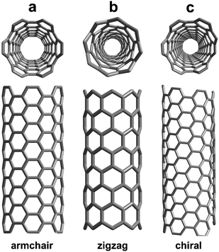 |
| | Fig. 1 Models of SWNTs exhibiting different chiralities: (a) armchair, (b) zig-zag, and (c) chiral arrangement. | |
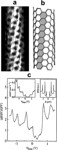 |
| | Fig. 2 (a) Atomically resolved STM image of an individual SWNT. The lattice on the cylinder surface allows identification of tube chirality by measuring the angle between the tube axis and the hexagon rows; (b) model of a chiral SWNT highlighting a hexagonal row; (c) (dI/dV)/(I/V), the measure of the DOS versus V for a semiconducting nanotube. The left inset displays the raw dI/dV data; the right inset displays the calculated DOS for a (16,0) semiconducting tube. The overall shape of the experimental peaks (van Hove singularities) resembles that predicted by theory. Reproduced from ref. 15 and 16. | |
2. Electron energy loss
2.1 General
Electron energy loss spectroscopy is based on the analysis of energy losses of initially quasi-monochromatic electrons subsequent to their interaction with a specimen.44 In general, an EELS experiment measures the number of electrons that lost an energy hω/2π and experienced a momentum change of hq/2π. The study of the inelastic scattering of electrons yields information on the nature of the elementary excitations of a crystalline structure, in a spatial region very close to the surface. Energy losses are mainly due to three processes: 1) excitations of lattice vibrations of atoms on a clean surface (surface optical phonons, surface acoustic phonons) and/or vibrations of atomic and molecular adsorbates. These losses are lower than 0.1 eV and, as a consequence, their effect on the energy spread of the quasi-monochromatic incident electron beam must be particularly small; 2) excitations of transitions involving electrons originating from the valence band (interband and intraband single-particle excitations, surface states, and volume, surface and interface plasmons). In the case of single particle processes and surface states, the energy losses are typically between few tenths of eV and few eV, while for plasmons the energies involved are between a few eV and tens of eVs; 3) core-level excitations, from which it is possible to perform a chemical, electronic and structural analysis in analogy with near edge X-ray absorption spectroscopy (XAS) and extended X-ray absorption fine structure (EXAFS). In this case, several hundreds of eVs are required to ionize core electrons. Experiments can be performed either in reflection or in transmission geometries. Here, we focus primarily on the transmission mode, which is generally performed inside a transmission electron microscope (TEM) equipped with an electron energy analyser, thereby allowing to acquire a spectroscopic signal with high spatial resolution. The spectral energy resolution is largely determined by the energy width of the electron source: 1–2 eV for a thermionic source, 0.5 to 0.7 eV for a field-emission gun (FEG) and 0.1–0.2 eV for a FEG followed by a monochromator. In particular, transmission EELS matches high spatial resolution and spectroscopy, allowing the direct collection of data from nanoscale fields of view (even individual nanostructures can be characterized). Nevertheless, the main drawback of these techniques is related to the possible local damage of the sample by the highly focused energetic electron beam (the energy is deposited in a volume of only few nm3). Electron induced damages can take a variety of forms, including dissociation, desorption, oxidization, reduction, polymerization, carbonization and diffusion depending on the specimen material and the gases present in the ultra high vacuum system.45 Therefore, particular care must be devoted to the investigation of nanostructures by EELS, so as to minimize electron beam damaging. Moreover, TEM images of the nanostructure under investigation should be taken before and after EELS analysis to ensure the quality of the acquired spectra. In the following sections we describe the conceptual principle of operation of transmission EELS under various regimes, while giving specific examples on how to apply it to the characterization of CNTs.
The description of the electron-excitation in a solid, both in the semi-classical and quantum mechanical framework, is based on the fact that the primary electron beam interacts with the long-range self-created Coulomb field induced by the charge-density fluctuations. Such charge-density fluctuations are correlated with the dielectric response, which is, in turn, a function of both frequency and wavevector of the external perturbation. Due to inelastic scattering, an electron in a solid can gain an energy value of hω/2π and an impulse of hq/2π, while the incident electron undergoes the corresponding losses in both energy and momentum. In the Born approximation, where the impinging and scattering electrons are considered as plane waves,44 the probability of absorbing such an energy loss ΔE = hω/2π and impulse hq/2π per unit path, in isotropic media, is given by:
| P(q,ω) = (2e2/(q2 π hv)) (−Im (εL−1(q,ω))) |
Where v is the electron velocity in the medium, εL(q,ω) is the longitudinal complex dielectric function (i.e., the response function of the medium to longitudinal fields, such as the one induced by the electrons). −Im (εL−1(q,ω)) is called the loss function and describes the volume loss for fast electrons in transmission experiments.
The charge density excitations can be of various types: (a) collective-plasmonic; (b) single particle interband and intraband; and (c) phononic (if the energy loss is very small). For highly anisotropic materials, the dielectric function is a tensor, which can be diagonalized to define in-plane and out-of-plane dielectric functions, giving thus rise to two different polarization directions, one with the momentum transfer (q) parallel to the basal plane, the other with q parallel to the crystallographic c axis. On the other hand, in optical absorption measurements, the spectra are obtained in terms of the absorption coefficient α, which is proportional to the imaginary part of the material's complex refraction index, i.e. to Im (εT1/2(q,ω)), where εT(q,ω) is the response function of the medium to transverse electromagnetic fields. Therefore, in the long wavelength limit (i.e. for small transferred momenta), the two techniques give similar information. In the framework of the classical Drude-Lorentz model, the loss peaks are always measured at up-shifted energies than the corresponding absorption peaks. This upshift is very large for bulk samples but can nearly vanish in the case of quasi-isolated nanoscale objects. In both cases, experimental features are strictly connected to the electronic properties of the system under study, since the imaginary part of the dielectric function can be obtained, to a first order approximation, from the convolution of valence and conduction density of states.46–48 Nevertheless, transmission EELS spectra acquired in a TEM apparatus present several advantages with respect to optical absorption measurements. These advantages include: 1) the possibility to directly image the area from which the electrons are collected and therefore, 2) the capability to select a specific region of the sample or nanostructure for investigation and/or to probe only a part of a nanostructure by reducing the size of the incident electron beam to a few nanometers; and 3) the ability to perform such measurements as a function of the momentum-transfer q.
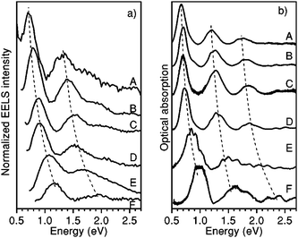
Experimentally, the dielectric response of graphite has been analyzed by both optical49–53 and EELS spectroscopies, and two characteristic features have been identified.54–61 In EELS experiments, the energy position and shape of both features depend on the modulus and orientation of the momentum transfer q. The former dependence is a fingerprint of the collective origin of these excitations. This allows to relate the peak in the 6–12 eV energy range to the collective excitations of the valence π electrons (π plasmon) and the feature located around 27 eV to those of all valence electrons (π + σ plasmon).56–58 Moreover, since crystalline graphite (as well as HOPG) is highly asymmetric, its dielectric function varies as a function of the angle θ between the transferred momentum q and the c-axis of the crystal. In particular, when q is oriented progressively closer to the c direction, both plasmon peaks downshift (while the π feature tends to disappear progressively) and the σ + π peak becomes more pronounced (Fig. 3, dotted lines).53,54,56,61 These effects enable to emphasize the importance of crystal field effects for out-of-plane orientations and have been interpreted as due to a strong confinement of the graphite layers, which can be essentially considered as isolated systems (Fig. 3, continuous lines).61 CNTs exhibit experimental EELS spectra similar to that of crystalline graphite, where the dominant structures are the π and the σ + π plasmons, though slightly downshifted with respect to their corresponding ones in graphite.62–71 Both π and σ + π plasmon features of CNTs are q dispersive and are highly anisotropic as a function of the q direction as for crystalline graphite, yet their shape and energy position have been shown to be also dependent on the number of walls of the nanotubes and/or on the number of SWCNTs forming the bundle. In particular, by performing transmission EELS measurements directly on a thin bundle of vertically aligned SWCNTs, as a function of the transferred momentum q, several observations can be made (Fig. 4). The π and π + σ plasmon peaks split into two distinct contributions; the first one is localized as in the case of a molecule and the second is dispersive, as in a crystalline solid. The non-dispersive peaks were interpreted as spatially confined plasmons perpendicular to the tube axis. On the other hand, the extrapolation of the π plasmon positions to the optical limit (q → 0) predicts values of 4.6 and 5.1 eV for the components parallel and perpendicular to the tube axis, respectively, in excellent agreement with polarized optical absorption measurements.72 Moreover, while the experimental dispersion behaviour of the π plasmon in crystalline graphite was found to be parabolic, it was measured to be linear for vertically aligned SWCNTs and intermediate between the two for bundles of SWCNTs. Theoretical ab initio calculations performed within the random phase approximation and accounting for local field effects succeeded in reproducing such trends, thus allowing to conclude that: 1) differences are mostly due to interactions between tubes; 2) interactions upshift the energy position of the π plasmon peak; and 3) for large q values no relevant difference can be observed among spectra of an individual SWCNT, a bundle of narrow vertically aligned tubes and SWCNT large bundles.71 These results confirmed calculations by Shyu and Lin, which also predicted the π plasmon energy upshift with increasing number of walls in a MWCNT.32 Similar upshifts of the energy position have been calculated for the on-axis component of the π + σ plasmon feature when considering interacting SWCNTs.73 Therefore, both π and π + σ plasmons can be considered as experimental fingerprints of the intertube distances and interactions in bundles of SWCNTs and of the intratube interactions in MWCNTs.63 In addition, when spectra are collected by using high resolution EELS, other types of electronic excitations, located at energies very close to the primary electron beam, can be detected both for SWCNTs64,66 and MWCNTs.34,35 In the former case, these excitations can be easily associated to electronic transitions between van Hove singularities in the electronic DOS of SWCNTs. In fact, their energy position does not vary with the momentum transfer q (i.e. are nondispersive) and is characteristic of the separation of the van Hove singularities of SWCNTs with different chirality. In Fig. 5, we report the experimental loss function, in this energy region, for SWCNTs with different mean diameters recorded with q = 0.1 Å−1 and corresponding optical absorption spectra (after background subtraction) for the same nanotubes.19 In particular, curves A, B, C, D, E and F refer to diameters of 1.46, 1.37, 1.34, 1.30, 1.08 and 0.91 nm, respectively. The close correspondence observed between the peaks of both panels of Fig. 5 can be definitively ascribed to lowest energy electronic interband transitions. More precisely, the EELS features (proportional to −Im(1/ε)) are slightly upshifted compared to the optical absorption ones which are proportional to Im(ε1/2). The experimental determination of the interband transition energies conclusively demonstrates that the standard theoretical approach to describe the electronic properties of SWCNTs (based on the tight binding method) is less accurate in the case of tube diameters smaller than 1.1 nm, since it neglects the influence of curvature on the carbon–carbon bonds. Another less studied spectral region is the low intensity shoulder of the π plasmon peak, located in the 3–4 eV energy range, which features a vanishingly small q dispersion.64,66 This shoulder is generally assigned to higher energy interband transitions that, due to their high number in this energy range, form an almost continuous broad feature.72 In samples where SWCNTs are packed in bundles, all these peaks are much smoother and lower in intensity32,73 so that the resulting feature, if observed, appears as a structureless shoulder of the π plasmons. These interband transitions are considered to be responsible for photocurrent generation in SWCNTs.74,75 For MWCNTs, it is generally thought that their electronic DOS is very smooth (similarly to graphite), and therefore should not present interband transitions at energies below the π plasmon, which would imply no associated photocurrent generation.34,35 However, by recording transmission EELS spectra directly on individual MWCNTs, we were able to identify the presence of well defined features at energies between 2.8 and 3.2 eV in addition to the typical π plasmon peak (Fig. 6). This pinpoints that the electronic DOS of the MWCNTs is considerably different from that of crystalline graphite and suggests the presence of singularities, due to the reduced dimensionality. These results have been theoretically confirmed by detailed EELS calculations predicting the existence of interband excitation channels in MWCNTs (Fig. 7).32 As in the case of SWCNTs, the intensity of this shoulder and its structure could vanish by increasing the number of walls constituting the nanotube,32 which should result in photocurrent intensity decrease.34 In sum, MWCNTs can generate a photocurrent under visible and near ultraviolet radiation and their photon conversion efficiency can reach up to 7% at the 350 nm excitation wavelength (a value 50 times higher than that showed by bare SWCNTs.34)
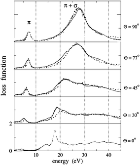 |
| | Fig. 3 Experimental EELS (dotted lines) acquired at q = 0.25 Å−1 as a function of the angle θ between the momentum transfer q and the c axis direction on HOPG and the calculations carried out within random phase approximation taking into account the crystal local field effects. Reproduced from Fig. 1 of ref. 61. | |
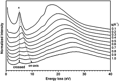 |
| | Fig. 4 Angle resolved loss-functions of vertically aligned-SWCNT at various momentum transfers 0.1 ≤ q ≤ 1.0. The dispersions of the two π plasmons are traced by dotted guides to the eye. Reproduced from Fig. 4 of ref. 70. | |
 |
| | Fig. 5 (a) Loss function in the region of the low-energy interband transitions for SWCNTs with six different diameters recorded with q = 0.1 Å−1. Curves A, B, C, D, E and F refer to diameters of 1.46, 1.37, 1.34, 1.30, 1.08 and 0.91 nm, respectively. (b) Optical absorption spectra (after background subtraction) from same SWCNT sample. Reproduced from Fig. 4 of ref. 19. | |
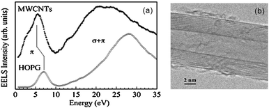 |
| | Fig. 6 (a) Transmission electron energy loss spectra measured collecting inelastic electrons from a HOPG very thin flake and a MWCNT. Note the shoulder in the MWCTNs spectra at energies lower than the plasmon π peak typical of the graphitic systems. (b) TEM image of the area of MWCNT from which electrons were collected. Unpublished results. | |
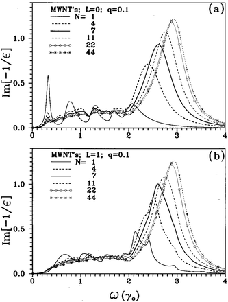 |
| | Fig. 7 (a) The loss spectra are shown for multiwall carbon nanotubes with different number of walls, N, at L = 0 and q = 0.1 Å−1. The (10,10) nanotube is the innermost tube of the MWCNTs; (b) same plot as the one displayed in the upper panel but for L = 1. L is the transferred angular momentum. Here γ0 = 2.4–2.7 eV. (Reproduced from Fig. 1 of ref. 32). | |
| −Im(1/ε) = ε2/(ε1 + ε2)2 ≈ ε2 |
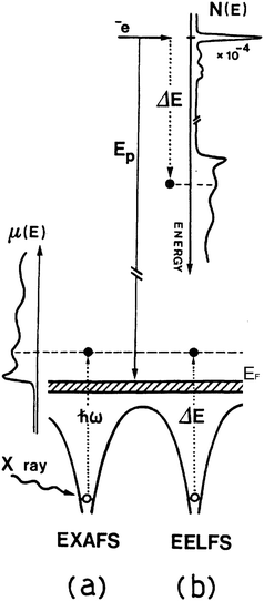
This means that the loss function occurs at the same frequency and assumes the same shape as ε2. On the other hand, the optical absorption coefficient (α) is also proportional to ε2 * hω/2π in this energy range. Therefore EELS spectroscopy directly provides the optical absorption coefficient, in the optical limit. The phenomenology of the EELS process is similar to that of the photoelectron generating a XAS feature. In the absorption process, the incident radiation (hν) selects the transition between the fundamental and the excited state (Fig. 8a). This imposes that the photon energy is continuously varied to measure the onset of the non-occupied states above EF. In EELS (Fig. 8b), the measured transition has a variable energy amplitude while the exciting energy remains strictly fixed. In this way, one measures the number of scattered electrons of the primary beam which have excited core electrons of the medium to the same interference final state of the X-ray absorption process. In particular, an estimate of the electron scattering cross section for high energy loss processes can be made within the framework of the Born approximation.76 This approximation generally holds when the velocity of the impinging electrons is much greater than that of the bound electrons in an orbital with the core radius ra. This means that the impinging and diffused electrons can be treated as plane waves. In the limit of q·ra « 1 (dipole approximation) the electron yield distribution N(E) of the measured scattered electrons is proportional to the differential cross section of the momentum q transferred to the excited electron by the primary electron beam, depending on the experimental scattering geometry77,78
| N(E) = dσ/dq ∝ q−1 |<ψf | εq·ra| ψi>|2 |
where
εq is the unit vector in the direction of
q vector and
ra is the atomic radius of the core electron. |ψ
i> and |ψ
f> are the electron wavefunctions describing the initial state and excited final state of the core electron, respectively. The above formula is very similar to the matrix element which appears in the X-ray absorption coefficient:
79| μ(E) ∝ |<ψf | ε·ra| ψi>|2 |
where
ε is the unit vector of the electric field in the direction of the X-ray polarization.
This means that, within the limit of the dipole approximation, EELS features are very similar in nature to the X-ray absorption spectroscopy (XAS) ones, obtained by synchrotron radiation excitation. Like XAS spectra, the EELS spectrum can be interpreted in two main energy loss ranges. The first region contains the ionization edge and presents features extending up to about 50 eV above the edge. It is named EELNES (electron energy loss near edge structure) region and like XANES (X-ray absorption near edge structure) it probes the unoccupied electronic states, allowed by the selection rules, over a wide energy range above the Fermi level. The second energy region starts at 50 eV or more, up to several hundred eV from the ionization edge and exhibits the so-called fine structure, in the form of weak intensity oscillations or local peaks. It is generally called extended energy-loss fine structure (EXELFS) and, like its equivalent for X-rays, the EXAFS (extended X-ray absorption fine structure) mainly contains information about the local atomic structure around the ionized atom. Thus, EXELFS spectra can be analyzed with the EXAFS data procedure.80,81
2.3.1 EELNES.
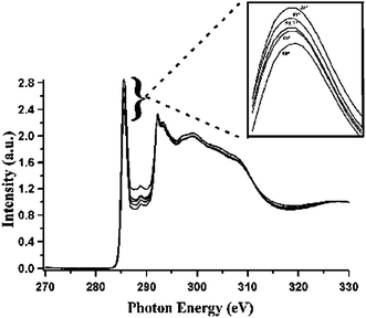
The XANES or EELNES carbon K edge spectra are due to the transition from the carbon 1s core level to p–like final unoccupied states and constitute therefore a fingerprint of the electronic DOS above the Fermi level. In graphite, they present a profile characteristic of sp2 bonded atoms, consisting of a sharp peak close to the absorption edge and a more structured feature at higher energy. The former peak is due to the transitions from 1s to π* antibonding states while the latter feature is associated with the 1s → σ* transitions.82–89 In crystalline graphite, the carbon K edge spectra strongly depend on the polarization vector ε direction, for XANES,85,87,89 and on the q direction in the energy loss case.83,88 As a consequence, when ε (or q) lies in the basal plane, final states of σ symmetry are detected while states of π symmetry are probed when ε (or q) is along the crystal c axis (Fig. 9).74 When spectra are acquired with very high energy resolution, a very sharp peak at ∼292.1 eV is also observed. This peak has been ascribed to a π* bound exciton (Fig. 10).87–89 Furthermore, some studies have shown that there is a significant symmetry mixing of higher energy σ* and σ* + π* orbitals.90 For crystalline samples, spectra are recorded at the so-called “magic angle”, corresponding to an angle of 55° between the ε (or q) and the crystal c axis, so as to eliminate polarization (or q direction) dependence effects. By measuring crystalline samples at the magic angle or polycrystalline and amorphous specimens at arbitrary angles, the intensity of the 1s →π* transition and its energy location can be considered as a measure of the amount of sp2 bonding. In fact, for an sp3-hybridized carbon network this peak is completely absent. However, such information is only qualitative. Most of the attempts made so far to quantify the sp3/sp2 hybridization ratio in carbon based materials have been proven to be inaccurate.91 Nevertheless, EELNES (and XANES) can detect changes in the local structure of the network, in terms of defects or sp3 bond introduction.92,93 In the latter perspective, attention has been paid to track the fingerprint, in the carbon K edge spectra, of the effects of graphite layers chirality, number of walls, bending, twisting, bundling and molecules interaction.90,93–109 One of the major advantages of EELNES compared to XANES, as mentioned above, is the latitude to choose precisely (at the nanoscale) the nanostructure (or part of it) one would like to investigate to obtain a close and direct connection between morphology and electronic properties. This has led, in particular, to highlight differences in the carbon K edge EELNES fine structure of typical crystalline graphite with respect to that collected from several carbon nanostructures, paying particular attention to the curvature effect in SWCNTs and MWCNTs.94,95 The left panel of Fig. 11 displays the carbon K edge fine structures corresponding to the various carbon nanostructures shown in the right panel. These studies suggest that the curvature, while not affecting the π* peak energy position, plays a key role in the variation of the σ* features, by decreasing the intensity of their first structure (b, see Fig. 11, left panel) and shifting all the other components (c, d, and e) towards low energies, which leads to their merging in a less defined, broad band. In addition, the observation of significant changes in the fine structure of carbon K energy loss near–edge structure spectra of SWCNT bundles with respect to the EELNES spectrum of an individual SWCNT suggests that structural arrangement effects (such as turning and twisting of SWCNTs into bundles) induce a sizeable interaction between tubes and give rise to the observed changes in the resulting electronic properties.101Fig. 12, left panel, displays EELNES spectra recorded at the carbon K edge for: an individual free–standing SWCNT, a free–standing bundle of aligned SWCNTs, two free–standing bundles of differently turned and twisted SWCNTs (namely, T1 and T2) and HOPG (the high resolution TEM images of these nanostructures are shown in Fig. 12 right panel). The π* peak for free-standing SWCNT is much narrower (∼1.6 eV) than that of bulk graphite (∼2.5 eV), of parallel packed SWCNTs (∼2.2 eV) and twisted/bundled SWCNTs (∼1.8 eV and ∼3 eV for T1 and T2, respectively). The carbon K edge spectra in the 293–340 eV energy range, probing the 1s → σ* transition, are also seen to change depending on the structure under observation. In general the peak positions are the same for individual SWCNTs and their bundles, however they are much sharper for an individual SWCNT than for a bundle of aligned SWCNTs. In other words, while curvature affects the energy position of the σ* states related peaks, tube bundling causes peak broadening. On the other hand, the anisotropy of CNTs has been evidenced by polarized XANES measurements on vertically aligned SWCNTs and MWCNTs mats89,103 and on individual MWCNTs.104 The former works suggested that polarization dependent XAS is an accurate, versatile, non destructive and reliable tool to quantify the alignment of SWCNTs on a bulk scale.89,103 These measurements also indicated that while the intensity of the C 1s → π* transition dramatically varies with X-ray orientations, the intensities of both the σ* bound exciton and that of the C 1s → σ* transitions remain insensitive or slightly dependent to the X-ray beam orientations, respectively (Fig. 13). This behaviour has been interpreted in terms of enhanced symmetry mixing of the higher energy σ* and σ* + π* states due to curvature-induced rehybridization effects in nanotubes.103,104 Moreover, it has been recently demonstrated that information on the location (within ≈ 25 nm) and densities of sp2-type defects can be obtained through X-ray absorption microscopy by mapping the intensity of the 1s → π* transition directly on individual MWCNTs. This opens up the prospect of using this technique in applications where the crystalline quality (absence/presence of defects) of the CNTs has to be monitored.104 On the other hand, recent high-resolution XANES experiments105 succeeded in revealing the electronic DOS of SWCNTs with their characteristic van Hove singularities (of which a spectroscopic signature is expected in the 1s → π* transition; see Fig. 14), in agreement with Fig. 14) theoretical calculations.106 Finally, the interaction of nanotubes with oxygen can be detected by presence of C–O and C![[double bond, length as m-dash]](https://www.rsc.org/images/entities/char_e001.gif) O resonances in the spectra in the 287–290 eV region.102,107 Likewise, nanotube functionalization can be probed by following the changes, induced by the anchored functional groups on CNT walls, in terms of energy positions and intensities of the spectral features.108
O resonances in the spectra in the 287–290 eV region.102,107 Likewise, nanotube functionalization can be probed by following the changes, induced by the anchored functional groups on CNT walls, in terms of energy positions and intensities of the spectral features.108
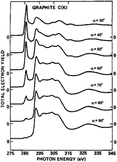 |
| | Fig. 9 Carbon K edge photoabsorption spectra of single-crystal graphite at various angle of incidence α, between the crystal c axis and the electric field unit vector ε of the light. (Reproduced from Fig. 1 of Ref. 85). | |
 |
| | Fig. 10 C–K edge XANES spectra of freshly cleaved HOPG. All the spectra have been pre and post edge normalized. Inset shows the geometry of π* vector orbitals and σ* planes with respect to the incident beam and the electric field E, which is always perpendicular to the incident X-ray irradiation. (Reproduced from Fig. 2 of ref. 89). | |
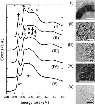 |
| | Fig. 11 Right panel: High resolution images displaying various morphologies of graphene layers in various carbon nanostructures (scale bar = 3nm). (I) a MWCNT consisting of well-stacked graphitized layer of 10–16 nm diameter; (II) coupled double layers in an aggregate of nanohorns of ∼3 nm; (III) an aggregate of various sized fullerenes (1–3nm), in which the adjacent fullerenes are decoupled with weaker interlayer interaction; (IV) double wall CNTs with well controlled diameters; (V) an isolated nanohorn consisting of a curved free standing graphene layer. Left panel: carbon K edge fine structures corresponding to the various carbon nanostructures shown in the right panel. (Reproduced from Figs. 2 and 3 of Ref. 94). | |
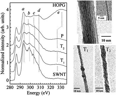 |
| | Fig. 12 Left panel: carbon K edge electron energy loss near edge structure of, from top to bottom, HOPG flake, a free-standing (P) parallel-packed SWCNTs bundle, two free standing coiled bundles of SWCNTs with two different type of twisting, a free-standing SWCNT. Right panel: TEM images of the nanostructures of which carbon K edges are shown in the left panel. The average diameter of SWCNTs is found to be (1.2 ± 0.2) nm while that of the bundle is (22 ± 2) nm. The average diameter of T1 and T2 bundles is (5.6 ± 0.5) nm and (6.0 ± 0.5) nm, respectively. Reproduced from ref. 101. | |
 |
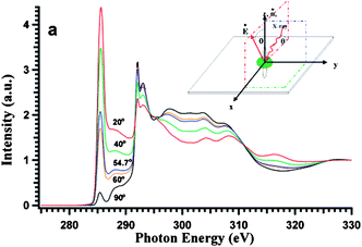
| | Fig. 13 Carbon K edge spectra of SWCNT bucky-paper. All the spectra have been pre- and post- edge normalized. Inset shows an expanded π* region. From the bottom to top, data corresponding to angles of incidence of 20°, 40°, 54.7°, 60°, 90°, respectively, are shown. (Reproduced from Fig. 3 of Ref. 89). | |
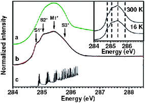 |
| | Fig. 14 Close-up of the high resolution C 1s absorption edges of (a) HOPG and (b) SWCNT and (c) diameter cumulative tight binding DOS, starting from the photoemission C 1s binding energy. The arrows indicate the features corresponding to the cumulative S1*, S2*, M1* and S3* van Hove transitions due to the several SWCNTs diameters with a Gaussian diameter distribution peaked at 1.37 nm with a spread of 0.08 nm. The inset depicts (b) at 16 K and ambient temperature, showing that no temperature dependence is observed. Note that the XANES curves have been acquired at a beam line with a resolving power E/ΔE of 4 × 10⁴. (Reproduced from Fig. 3 of Ref. 105). | |
2.3.2 EXELFS.
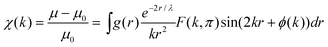
In EXAFS-like cases, the oscillatory behaviour of the absorption coefficient μ is described, for a K-edge, by the following relation:80,81
where: r is the interatomic distance, g(r) is the radial distribution function, k is the wave vector, F(k,π) is the backscattering amplitude, λ(k) is the mean free path of the emitted electron, e−2r/λ describes the inelastic diffusion of the photoelectron and ϕ(k) is the total phase shift. In the standard EXAFS formalism, the pair distribution function g(r) is characterized by a Gaussian shape with broadening depending on the Debye–Waller factor, σ, that takes into account the atomic thermal vibration around the equilibrium position.109,110
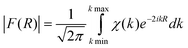
The structural analysis is performed through the Fourier Transform of the experimental signal χ(k), as follows:
In EXAFS-like processes, the excited atom acts as a source as well as a
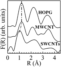
detector, and thus the F(R) curve shows peaks which are related to the different atomic shells at distance R(Å) surrounding the ionized atom located at the origin of the scale.
The basic assumption underlying the validity of the reported EXAFS formula is to neglect multiple scattering events, i.e. by neglecting the scattering function F(k) at angles different from the backwards direction. However, these events have been demonstrated to be often fundamental to satisfactorily describe the mechanism underlying the ionization process. Therefore, in the χ(k) calculations, one should take into account not only contributions from 2-body entities (i.e. pairs) but also those originating from higher order events (for example, triplets and quadruplets of atoms beginning and ending on the ionized atom).111
The analysis of EXAFS-like signals of low-Z absorbers (e.g. C, N, and O) involving low-Z atom scatterers presents a number of difficulties because in this case EXAFS oscillations are fewer and less intense than for high-Z atoms. This occurs because light element bonds are very short and their amplitude rapidly decreases above the absorption edge. While HOPG has been investigated by both EXAFS82,86,112,113 and EXELFS,83,84 only a few studies at the carbon K edge on CNTs have been reported.114,115 In contrast, using hard X-rays, EXAFS can be employed to investigate heavier elements inside CNTs, such as iron,116 cobalt117,118 or iodine.119 The analysis of such EXAFS data can easily lead to better understand the relationship between nanotube growth conditions (at a particular temperature) and iron or cobalt nanoparticle structure,116–118 or to study the effect of iodine doping on CNTs.119
The study of the extended fine structure well above the carbon K edge has always been considered a highly challenging task. In the early work, signals were analysed by taking into account only the backscattering of the excited core electrons by the nearest neighbour atoms (i.e. the single scattering regime) and neglecting any other scattering path involving more than two atoms. Although such analyses82–84,86,112,113 yield the first shell coordination numbers and their corresponding C–C bond lengths, they have definitively failed in reproducing the EXAFS like signal in the entire k wavevector range and in particular for k values <6 Å−1. On the other hand, almost all the EELS spectra (above the carbon K edge) reported so far have been acquired over a very narrow energy window (Emax about 550 eV), which considerably limits the information that can be extracted from the EXELFS oscillations. Recently, we have investigated the EXELFS signals of HOPG, SWCNTs and MWCNTs, over an EXELFS spectral range of up to 11 Å−1, with a good signal to noise ratio and no oxygen contaminants.114,115 The dipole approximation is valid under these experimental conditions115 and therefore the EXELFS signal was analysed by using the EXAFS data procedure.121,122Fig. 15 displays the spectral features collected at the carbon K edge for the HOPG thin flake, a rope of parallel-assembled SWCNTs and a MWCNT. Particular care was taken to record the EELS spectra at the carbon K edge only from the SWCNTs rope and from isolated MWCNTs, thus avoiding the collection of electrons originating from any catalyst particles and/or carbonaceous products other than nanotubes. Moreover, the absence of any EELS signal at the L2,3 edges of Ni and Co ensured the absence of catalyst atoms and clusters in the SWCNTs analyzed samples. In addition, prior to EELS observations the SWCNTs bundle was specifically chosen in the TEM assumed to be formed by straight and well aligned parallel nanotubes, so as to minimize the contribution of structural defects (such as pentagons and/or heptagons) in their hexagonal network. Such structural defects have been shown to produce coiled, bent, or twisted ropes of SWCNTs101,120 and to induce different carbon K near edge signals.101 No features of either nitrogen or oxygen K edges, at 410 and 530 eV, respectively, were detected in our EELS spectra. This is another crucial criterion to be fulfilled to avoid any structural defects that can be created by the presence of nitrogen and/or oxygen in the nanotube cage. Fig. 16 shows the EXELFS signals, kχ(k), of the HOPG thin flake, a rope of parallel-assembled SWCNTs and a MWCNT, after background subtraction. Changes in the amplitude and phase can be clearly seen mainly for the SWCNTs sample compared to HOPG. (Fewer differences are recognizable between MWCNT and HOPG.) To further investigate the origin of the observed changes, we simulated the EXELFS data of HOPG and SWCNTs by using the FEFF8.2 software that calculates the extended X-ray absorption fine structure.121 Thus, to reproduce accurately the HOPG and SWCNTs oscillations over all the k range, we have demonstrated that it is essential to consider a very large number of atoms around the ionized one together with a multiple scattering approach involving up to eight body scattering. In addition, we have shown that the EXELFS signal is a fingerprint of the SWCNTs chirality (Fig. 17). This is the only technique known so far to access directly the chirality of a nanotube if sufficient care is spent on the acquisition of the EXELFS spectrum from an individual SWCNT (i.e. it does not average over many tubes). Finally, the Fourier transforms, F(R), of the EXELFS signals (shown in Fig. 16) yielded interesting information. Indeed, the F(R) curves (Fig. 18) are seen to consist of three prominent peaks between 0.5 and 4.2 Å, corresponding, within the single scattering approach, to the first nearest neighbors both in the basal plane and out-of-plane, in good agreement with the literature.83,84,86 Nevertheless, it should be emphasized that the observed peak position in the F(R) does not correspond exactly to the first neighbors distance of graphite (obtained through electron and X-ray diffraction experiments) because of the phase shift, ϕj(k), present in the EXAFS formula, that should be properly introduced to fit the F(R).83,122,123 Consequently, for example, the first nearest neighbour appears at 1.2 Å in the F(R) instead of the 1.42 Å lattice atomic position value of graphite. A comparison of the F(R) curves of Fig. 18 reveals a decrease of 0.15 Å in the location of the first coordination shell for the SWCNTs with respect to those of either HOPG or MWCNT. At first glance this feature can be interpreted as a C–C bond length contraction. However, neither electron diffraction measurements nor stability calculations evidenced such a C–C bond length contraction for CNTs with diameter greater than 1 nm.124–126 On the other hand, although we devoted particular care to the choice of freestanding, straight, continuous parallel-packed SWCNTs with the absence of any elemental impurity (such as N or O), the presence of random distortions and/or structural defects in the SWCNT hexagonal network cannot be absolutely excluded. Yet, no contraction of C–C first coordination shell has been observed in the case of amorphous carbon (a–C) films, where higher bond angle distortions are expected.82,86,113 If the C–C first neighbor position does not change in a–C films, it would not be affected in CNTs, where the bond angle distortions and/or curvature experienced by the C–C bonds are less strong than in a–C films. Conversely, an apparent contraction of the lattice parameter has been already observed by EXAFS (or EXELFS) in the case of low-Z adsorbates.127,128 This has been interpreted as a consequence of enhanced out-of-plane vibrations of the atoms giving rise to an anharmonic pair potential and an asymmetric pair distribution function, g(R). In fact, this anharmonicity enters in the EXAFS formalism, making the EXAFS-like data particularly sensitive to any variation in the shape of the g(R) function. Interestingly, the downward shift of the first peak in the F(R) of SWCNTs was found to be slightly dependent on the number of tubes that form the bundle. This is illustrated in Fig. 19 where the nearest-neighbour positions in the F(R) curves are compared for two bundles of parallel SWCNTs with two different diameters, namely, 22 ± 2 and 5 ± 1 nm (formed by a maximum of 340 and 18 nanotubes, respectively). The TEM image of the latter bundle is shown in the inset of Fig. 19. In fact, the shift of the F(R) peak is of ∼0.03 ± 0.02 Å toward lower R values, when passing from a bundle of ∼340 tubes to the one of ∼18. This shows that a considerable reduction of the number of nanotubes in the bundle slightly decreases the reported apparent contraction. In other words, the radial motion of the C atoms in SWCNTs seems to be slightly affected by the number of the tubes in the rope. Ultimately, such an anharmonic effect could be slightly enhanced and eventually reaches its maximum in a single tube. Based on these findings, we anticipate that a similar effect can be observed in the case of MWCNTs with a very low number of walls. The one probed in our case has a number of walls (12 walls) which is highly likely too high to lead to any observable anharmonic effects arising from surface atoms. Also, as the number of walls increases in MWCNTs, their associated diameter increases and consequently the C–C bonds experience less curvature effects. As the anharmonic effect is not accounted for in the theoretical model that simulates the EXELFS spectra (the calculated χ(k) signals account for dynamical atomic motion only through the Debye–Waller factor), it is not surprising to observe such a discrepancy (position shift of the first neighbour) between the experimental and simulated data. To account for this anharmonic effect, we estimated the degree of asymmetry of the g(R) for HOPG and SWCNTs (MWCNTs are non distinguishable from HOPG) along the lines of a simple model using the following formula to calculate the contribution of the first nearest neighbours to the χ(k) signal:129,130
| χ1(k) = ∫g(R)e−2R/λA1(k,π)/kR2 sin(2kR1 + Φ1(k))dR |
where the scattering amplitude
A1(
k, π) and the phase shift Φ
1(
k) of the carbon atom first nearest neighbours are extracted from the experimental HOPG
spectrum. The same
A1(
k, π) and Φ
1(
k) values were used for SWCNTs, since the simulated ones result to assume the same values in all the
k wavevector range, thus establishing the complete amplitude and phase transferability of the C–C EXELFS signal for carbon atoms in slightly different structures. The value of
R1 was chosen to be 1.42 Å. The mean free path
λ has been considered to have a linear dependence on the wavevector
k,
131 and the pair distribution function
g(
R) to be as follows:
where
U(
R) is assumed to be a Morse potential of the following form:
132,133| U(R) = D(e−2R(R−R1) − 2e−R(R−R1)) |
where the binding energy,
D, was considered to be of 1 eV/atom and the measurements were performed at room temperature. The values for the R parameter giving rise to the Fourier transforms that best reproduce the
experimental data recorded for both the 22 and 5 nm bundles were evaluated through an iterative process. We found that α for
graphite is 2.00 ± 0.01 Å
−1, whereas for the bundle of SWCNTs of 22 and 5 nm diameter it is 0.62 ± 0.01 Å
−1 and 0.60 ± 0.01 Å
−1, respectively.
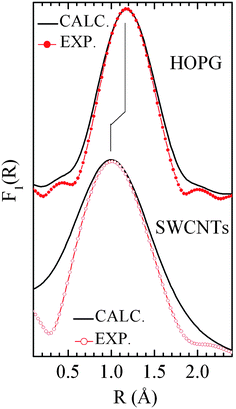
Fig. 20 displays the comparison between the experimental and simulated
F1(
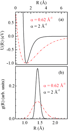
R) curves for HOPG and the 22 nm diameter bundle, showing that a perfect fit is obtained.
Fig. 21a and 21b show the respective potential
U(
R) and the corresponding
g(
R) used to obtain the result of
Fig. 20. The α value for
graphite is high enough to make the
g(
R) curve symmetric, whereas the latter value (for SWCNTs) is necessary to shift the
F1(
R) peak toward lower
R values. As mentioned above, information on the anharmonicity of carbon atoms on the SWCNT surface is expected to be at its maximum if an EXELFS
spectrum is recorded on an isolated
nanotube. This is consistent with the interpretation of the energy downshift of the plasmon peaks by decreasing the number of SWCNTs constituting the bundle or the number of walls forming a MWCNT.
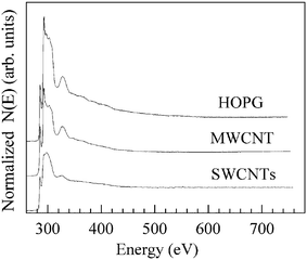 |
| | Fig. 15 Spectral features collected at the carbon K edge for the HOPG thin flake, a rope of parallel-packed SWCNTs and a MWCNT. Particular care has been taken to record the EELS spectra at the carbon K edge only from the SWCNTs rope and from isolated MWCNTs, thus avoiding to collect electrons coming from any catalyst particles and/or carbonaceous products other than nanotubes. No nitrogen or oxygen K edge related features (at 409 and 530 eV, respectively) can be detected in all the three spectra. Reproduced from Fig. 2 of ref. 114. | |
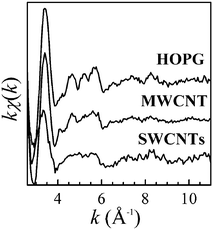 |
| | Fig. 16 EXELFS signals, kχ(k), of the HOPG thin flake, the SWCNTs bundle and the MWCNT of which carbon K edges are shown in Fig. 15. Reproduced from Fig. 3 of ref. 114. | |
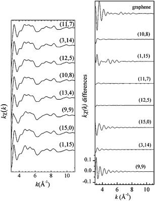 |
| | Fig. 17 Left panel: kχ(k) simulated signals for a graphene layer and for SWCNTs having a diameter of ∼1.2 nm but with different (n,m) helicities. All the simulations were performed by fixing the cluster radius to 8 Å and accounting for all the multiple scattering paths contributions of up to eight bodies. Right panel: differences between the EXELFS theoretical calculation of each chirality SWCNTs reported in panel (a) with one of them (e.g., the (13, 4) in the present case). The y-scale is the same for all the differences as that shown in the bottom figure. Reproduced from ref. 115. | |
 |
| | Fig. 18 Fourier transforms, F(R), of the kχ(k) oscillations shown in Fig. 16. The k range for the F(R) curve calculations extends from approximately kmin = 4.4 Å−1 to kmax = 11 Å−1. Reproduced from Fig. 3 of ref. 114. | |
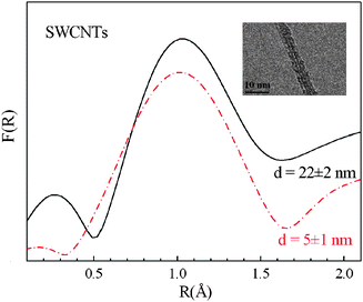 |
| | Fig. 19 Fourier transform curves for two bundles of parallel SWCNTs with two different diameters, d: d = 22 ± 2 nm (solid black line) and d = 5 ± 1 nm (dot-dashed red line). Inset: high-resolution TEM images of the latter SWCNT bundle investigated by EXELFS. The bundles are seen to be formed by parallel alignment of SWCNTs. The TEM image of the former bundle has been reported in the right panel of Fig. 12. Reproduced from ref. 115. | |
 |
| | Fig. 20 Fourier transforms of the experimental kχ(k) compared to those calculated taking into account the asymmetry of the g(R) function. The best fit is obtained for α = 2 Å−1 and α = 0.62 Å−1 for HOPG and SWCNT bundle of 22 nm diameter, respectively. Reproduced from ref. 115. | |
 |
| | Fig. 21 Comparison of Morse potential (a) and g(R) function (b) calculated for two different a values: α = 2 Å−1 (solid black curves) corresponding to HOPG and α = 0.62 Å−1 (dot-dashed red curves) corresponding to the 22 nm diameter bundle of SWCNTs. Reproduced from ref. 115. | |
3. Conclusions and perspectives
In this feature article, we have reviewed the investigation of the electronic structure of CNTs by local electron spectroscopies, while comparing the results, whenever relevant, to HOPG reference material. In particular we have highlighted the complementary role of EELS techniques with respect to other widely used optical and X-ray absorption spectroscopies. This has been illustrated by showing how EELS spectra analysis can provide valuable structural/electronic information on CNTs which essentially cannot be accessed by any other technique. In principle STM and STS measurements allow to obtain similar information, however in such cases the substrate may play an important role. EELS spectra acquired in transmission have the additional advantage of being acquired on free standing tubes in pristine conditions and with no influence of a substrate.
A salient example is the direct access of nanotube chirality through a careful EXELFS spectrum acquisition and analysis. Such information becomes very accurate if the EXELFS spectrum is taken from an individual SWCNT. EELS transmission techniques offer the outstanding advantage of imaging and eventually singling out a specific nanostructure for investigation at the nanoscale (few square nanometers). This “privileged” local access to the information originating from a single nanostructure contrasts with the other techniques that mainly yield information originating from larger area (thus reflecting the average behaviour of a significant number of structures present in the sample rather than individual structures), such as e.g. Tip Enhanced Raman Scattering, Rayleigh Scattering and Raman Scattering coupled to Scanning Near Field Optical Microscopy. We also discussed how transmission EELS allows to extract interesting information on the inter- or intra-tube distances and interactions in SWCNTs bundles or MWCNTs, respectively. Finally, we demonstrated the use of EXELFS signals to identify the presence of defects, functional groups and/or chemical interaction with contaminants in the CNTs nanostructure. This has led, in particular, to emphasize the more pronounced anharmonicity effects in SWCNTs compared to MWCNTs. It is clear that accessing directly the local C–C bonding topologies in CNTs and related electronic structure will undoubtedly contribute to a more fundamental understanding of the CNTs which, in turn, will foster the exploitation of their full potential in nanotechnology applications.
Acknowledgements
We thank the Italian Foreign Affairs Ministry through Promotion and Cultural Cooperation Management and the Ministère pour le Developpement Economique, l'Innovation et l'Exportation (MDEIE, Quebec) for financial support. F.R. is grateful to the Canada Research Chairs program for partial salary support. M.A.E and F.R. also acknowledge the financial support from The Natural Science and Engineering Research Council (NSERC) of Canada and the Fonds Québecois de la Recherche sur la Nature et les Technologies (FQRNT) of Québec.
References
- H. W. Kroto, J. R. Heath, S. C. O'Brien, R. F. Curl and R. E. Smalley, Nature, 1985, 318, 162 CrossRef CAS.
-
R. Saito, G. Dresselhaus, M. S. Dresselhaus in Physical Properties of Carbon Nanotubes, Imperial College Press, 2000 Search PubMed.
- A. Oberlin, M. Endo and T. Koyama, J. Cryst. Growth, 1976, 32, 335 CrossRef CAS.
- S. Iijima, Nature, 1991, 354, 56 CrossRef CAS.
- G. Fanchini, H. E. Unalan and M. Chhowalla, Appl. Phys. Lett., 2006, 88, 191919 CrossRef.
- P. Avouris, Acc. Chem. Res., 2002, 35, 1026 CrossRef CAS.
- S. J. Tans, A. R. M. Verschueren and C. Dekker, Nature, 1998, 393, 49 CrossRef CAS.
- R. Martel, T. Schmidt, H. R. Shea, T. Hertel and P. Avouris, Appl. Phys. Lett., 1998, 73, 2447 CrossRef CAS.
- M. Bockrath, D. H. Cobden and P. L. McEuen, Science, 1997, 275, 1922 CrossRef CAS.
- B. Aissa and M. A. El Khakani, Nanotechnology, 2009, 20, 175203 CrossRef CAS.
- J. W. Mintmire, B. I. Dunlap and C. T. White, Phys. Rev. Lett., 1992, 68, 631 CrossRef CAS.
- N. Hamada, S. I. Sawada and A. Oshiyama, Phys. Rev. Lett., 1992, 68, 1579 CrossRef CAS.
- S. Saito, Science, 1997, 278, 77 CrossRef CAS.
-
M. S. Dresselhaus, G. Dresselhaus, P. Eklund in Science of Fullerenes and Carbon Nanotubes, ed. Academic Press, San Diego, 1996 Search PubMed.
- J. W. G. Wildoer, L. C. Venema, A. G. Rinzler, R. E. Smalley and C. Dekker, Nature (London), 1998, 391, 59 CrossRef CAS.
- T. W. Odom, J. L. Huang, P. Kim and C. M. Lieber, Nature (London), 1998, 391, 62 CrossRef CAS.
- J. Chen, M. A. Hamon, H. Hu, Y. Chen, A. M. Rao, P. C. Eklund and R. C. Haddon, Science, 1998, 282, 95 CrossRef CAS.
- H. Kataura, Y. Kumazawa, Y. Maniwa, I. Umezu, S. Suzuki, Y. Ohtsuka and Y. Achiba, Synth. Met., 1999, 103, 2555 CrossRef CAS.
- X. Liu, T. Pichler, M. Knupfer, M. S. Golden, J. Fink, H. Kataura and Y. Achiba, Phys. Rev. B, 2002, 66, 045411 CrossRef.
- A. M. Rao, E. Richter, S. Bandow, B. Chase, P. C. Eklund, K. A. Williams, S. Fang, S. K. R. Subbaswamy, M. Menon, A. Thess, R. E. Smalley, G. Dresselhaus and M. S. Dresselhaus, Science, 1997, 275, 187 CrossRef CAS.
- H. Kuzmany, W. Plank, M. Hulman, Ch. Kramberger, A. Gruneis, Th. Pichler, H. Peterlik, H. Kataura and Y. Achiba, Eur. Phys. J. B, 2001, 22, 307 CrossRef.
- M. S. Dresselhaus, G. Dresselhaus, A. Jorio, A. G. Souza Filho, M. A. Pimenta and R. Saito, Acc. Chem. Res., 2002, 35, 1070 CrossRef CAS.
- M. O'Connell, S. M. Bachilo, C. B. Huffman, V. Moore, M. S. Strano, E. Haroz, K. Rialon, P. J. Boul, W. H. Noon, C. Kittrell, J. Ma, R. H. Hauge, R. B. Weisman and R. E. Smalley, Science, 2002, 297, 593 CrossRef CAS.
- S. M. Bachilo, M. S. Strano, C. Kittrell, R. H. Hauge, R. E. Smalley and R. B. Weisman, Science, 2002, 298, 2361 CrossRef CAS.
- R. Saito, G. Dresselhaus and M. S. Dresselhaus, J. Appl. Phys., 1993, 73, 494 CrossRef CAS.
- J.-C. Charlier and J.-P. Michenaud, Phys. Rev. Lett., 1993, 70, 1858 CrossRef CAS.
- Ph. Lambin, L. Philippe, J. C. Charlier and J. P. Michenaud, Comput. Mater. Sci., 1994, 2, 350 CrossRef CAS.
- Y.-K. Kwon, Y. H. Lee, S. G. Kim, P. Jund, D. Tománek and R. Smalley, Phys. Rev. Lett., 1997, 79, 2065 CrossRef CAS.
- J.-C. Charlier, A. De Vita, X. Blase and R. Car, Science, 1997, 275, 646 CrossRef.
- M. Buongiorno Nardelli, C. Brabec, A. Maiti, C. Roland and J. Bernholc, Phys. Rev. Lett., 1998, 80, 313 CrossRef.
- Y.-K. Kwon and D. Tománek, Phys. Rev. B, 1998, 58, R16001 CrossRef CAS.
- F. L. Shyu and M. F. Lin, Phys. Rev. B, 2000, 62, 8508 CrossRef CAS.
- X. Wang and H. K. Yang, Phys. Rev. B, 2006, 73, 085409 CrossRef.
- P. Castrucci, F. Tombolini, M. Scarselli, E. Speiser, S. Del Gobbo, W. Richter, M. De Crescenzi, M. Diociaiuti, E. Gatto and M. Venanzi, Appl. Phys. Lett., 2006, 89, 253107 CrossRef.
- M. Passacantando, F. Bussolotti, V. Grossi, S. Santucci, A. Ambrosio, M. Ambrosio, G. Ambrosone, V. Carillo, P. Maddalena, E. Perillo and A. Raulo, Appl. Phys. Lett., 2008, 93, 051911 CrossRef.
- M. A. El Khakani, V. Le Borgne, B. Aissa, F. Rosei, C. Scilletta, E. Speiser, M. Scarselli, P. Castrucci and M. De Crescenzi, Appl. Phys. Lett., 2009, 95, 083114 CrossRef.
- M. Scarselli, C. Scilletta, F. Tombolini, P. Castrucci, M. De Crescenzi, M. Diociaiuti, S. Casciardi, E. Gatto and M. Venanzi, Superlattices and Microstructures, 2009, 46, 340 CrossRef CAS.
- M. Scarselli, C. Scilletta, F. Tombolini, P. Castrucci, M. Diociaiuti, S. Casciardi, E. Gatto, M. Venanzi and M. De Crescenzi, J. Phys. Chem. C, 2009, 113, 5860 CrossRef CAS.
- B. K. Sarker, M. Arif, P. Stokes and S. I. Khondaker, J. Appl. Phys., 2009, 106, 074307 CrossRef.
- S. Frank, P. Poncharal, Z. L. Wang and W. A. de Heer, Science, 1998, 280, 1744 CrossRef CAS.
- C. Gómez-Navarro, P. J. De Pablo, J. Gómez-Herrero, B. Biel, F. J. Garcia-Vidal, A. Rubio and F. Flores, Nat. Mater., 2005, 4, 534 CrossRef CAS.
- L. Valentini, F. Mercuri, I. Armentano, C. Cantalini, S. Picozzi, L. Lozzi, S. Santucci, A. Sgamellotti and J. M. Kenny, Chem. Phys. Lett., 2004, 387, 356 CrossRef CAS.
- M. S. Raghuveer, A. Kumar, M. J. Frederick, G. P. Louie, P. G. Ganesan and G. Ramanath, Adv. Mater., 2006, 18, 547 CrossRef CAS.
-
(a)
M. De Crescenzi, M. N. Piancastelli, in “Electron Scattering and Related Spectroscopy”, ed. World Scientific Publishing Co., Singapore, 1996 Search PubMed;
(b) M. De Crescenzi, Surf. Sci. Rep., 1995, 21, 89 CrossRef CAS.
- C. J. Humphreys, Ultramicroscopy, 1989, 28, 357 CrossRef and references therein.
- H. Ehrenreich and H. R. Philip, Phys. Rev. B, 1962, 128, 1622 Search PubMed.
- R. Lässer, N. V. Smith and R. L. Benbow, Phys. Rev. B, 1981, 24, 1895 CrossRef CAS.
- R. Lässer, N. V. Smith and S. Chiang, Phys. Rev. B, 1982, 25, 806 CrossRef.
- E. Taft and H. R. Philipp, Phys. Rev., 1965, 138, A197 CrossRef.
- H. Venghaus, Phys. Status Solidi B, 1975, 71, 615 CrossRef.
- D. L. Greenaway, G. Harbeke, F. Bassani and E. Tosatti, Phys. Rev., 1969, 178, 1340 CrossRef CAS.
- G. Guizzetti, L. Nosnezo, E. Reguzzoni and G. Samoggia, Phys. Rev. Lett., 1973, 31, 154 CrossRef CAS.
- R. Klücker, M. Skibowski and W. Steinmann, Phys. Status Solidi B, 1974, 65, 703 CrossRef CAS.
- K. Zeppenfeld, Phys. Letters A, 1967, 25, 335 Search PubMed.
- K. Zeppenfeld, Z. Phys., 1968, 211, 391 Search PubMed.
-
J. Daniels, C. von Festenberg, M. Raether, K. Zeppenfeld in “Optical constant of Solids by electron spectroscopy”, Springer Tracts in Modern Physics 54, ed. Springer-Verlag, New York, 1970 Search PubMed.
- K. Zeppenfeld, Z. Phys., 1971, 243, 229 Search PubMed.
- U. Büchner, Phys. Status Solidi (b), 1977, 81, 227 CrossRef.
- N. Papageorgiou, M. Portail and J. M. Layet, Surf. Sci., 2000, 454–456, 462 CrossRef CAS.
- M. Vos, A. S. Kheifets, E. Weigold and F. Aryasetiawan, Phys. Rev. B, 2001, 63, 033108 CrossRef.
- A. G. Marinopoulos, L. Reining, V. Olevano, A. Rubio, T. Pichler, X. Liu, M. Knupfer and J. Fink, Phys. Rev. Lett., 2002, 89, 076402 CrossRef CAS.
- P. M. Ajayan, S. Iijima and T. Ichihashi, Phys. Rev. B, 1993, 47, 6859 CrossRef CAS.
- L. A. Bursill, P. A. Stadelmann, J. L. Peng and S. Prawer, Phys. Rev. B, 1994, 49, 2882 CrossRef CAS.
- T. Pichler, M. Knupfer, M. S. Golden, J. Fink, A. Rinzler and R. E. Smalley, Phys. Rev. Lett., 1998, 80, 4729 CrossRef CAS.
- B. W. Reed and M. Sarikaya, Phys. Rev. B, 2001, 64, 195404 CrossRef.
- X. Liu, T. Pichler, M. Knupfer, M. S. Golden, J. Fink, D. A. Walters, M. J. Casavant, J. Schmidt and R. E. Smalley, Synthetic Metals, 2001, 121, 1183 CrossRef CAS.
- O. Stéphan, D. Taverna, M. Kociak, K. Suenaga, L. Henrard and C. Colliex, Phys. Rev. B, 2002, 66, 155422 CrossRef.
- R. B. Chen, C. P. Chang, C. H. Lee and M. F. Lin, J. Appl. Phys., 2007, 101, 114305 CrossRef.
- M. Dapor, L. Calliari and M. Filippi, Nucl. Instr. Meth. Phys. Res. B, 2007, 255, 276 CrossRef CAS.
- C. Kramberger, M. Rümmeli, M. Knupfer, J. Fink, B. Bücnher, E. Einarsson, S. Maruyama and T. Pichler, Phys. Stat. Solidi, 2008, 245, 2284 Search PubMed.
- C. Kramberger, R. Hambach, C. Giorgetti, M. H. Rümmeli, M. Knupfer, J. Fink, B. Bücnher, L. Reining, E. Einarsson, S. Maruyama, F. Sottile, K. Hannewald, V. Olevano, A. G. Marinopoulos and T. Pichler, Phys. Rev. Lett., 2008, 100, 196803 CrossRef CAS.
- Y. Murakami, E. Einarsson, T. Edamura and S. Maruyama, Phys. Rev. Lett., 2005, 94, 087402 CrossRef.
- A. G. Marinopoulos, L. Reining, A. Rubio and N. Vast, Phys. Rev. Lett., 2003, 91, 046402 CrossRef CAS.
- S. Barazzouk, S. Hotchandani, K. Vinodgopal and P. V. Kamat, J. Phys. Chem. B, 2004, 108, 17015 CrossRef CAS.
- A. Mohite, G. U. Sumanasekera, K. Hirahara, S. Bandow, S. Iijima and B. W. Alphenaar, Chem. Phys. Lett., 2005, 412, 190 CrossRef CAS.
-
L. Landau, E. Lifschitz, in Mécanique Quantique, Théorie non Relativiste 3rd Edition ed. MIR, Moscow, 1974 Search PubMed.
- R. D. Leapmann, P. Rez and D. F. Mayers, J. Chem. Phys., 1980, 72, 1232 CrossRef.
- R. D. Leapmann, L. A. Grunes and P. L. Fejes, Phys. Rev. B, 1982, 26, 614 CrossRef.
-
S. Gasiorowicz, in Quantum Physics, ed. Wiley, New York, 1974 Search PubMed.
- P. A. Lee, P. M. Citrin, P. Esenberger and B. M. Kincaid, Rev. Mod. Phys., 1981, 53, 769 CrossRef CAS.
- For reviews of EXAFS spectroscopy, see EXAFS spectroscopy, Techniques, and Applications, edited by B. K. Teo and D. C. Joy, Plenum Press, New York, 1981 Search PubMed;
B. K. Teo, EXAFS: Basic Principles and Data Analysis, Inorganic Chemistry Concepts 9, ed. Springer-Verlag, Heidelberg, 1986 Search PubMed.
- D. Denley, P. Perfetti, R. S. Williams, D. A. Shirley and J. Stöhr, Phys. Rev. B, 1980, 21, 2267 CrossRef CAS.
- B. M. Kinkaid, A. E. Meixner and P. M. Platzman, Phys. Rev. Lett., 1978, 40, 1296 CrossRef.
- M. M. Disko, O. L. Krivanek and T. Rez, Phys. Rev. B, 1982, 25, 4252 CrossRef CAS.
- R. A. Rosenberg, P. J. Love and V. Rehn, Phys. Rev. B, 1986, 33, 4034 CrossRef CAS.
- G. Comelli, J. Stöhr, C. J. Robinson and W. Jark, Phys. Rev. B, 1988, 38, 7511 CrossRef CAS.
- Y. Ma, P. Skytt, N. Wassdahl, P. Glans, D. C. Mancini, J. Guo and J. Nordgren, Phys. Rev. Lett., 1993, 71, 3725 CrossRef CAS.
- P. A. Brühwiler, A. J. Marshall, C. Puglia, A. Nilsson, S. Andersson and N. Mårtensson, Phys. Rev. Lett., 1995, 74, 614 CrossRef.
- S. Banerjee, T. Hemraj-Benny, S. Sambasivan, D. A. Fisher, J. A. Misewich and S. S. Wong, J. Phys. Chem. B, 2005, 109, 8489 CrossRef CAS.
- A. Y. Sokolov, E. Z. Kurmaev, J. MacNaughton, A. Moewes, N. A. Skorikov and L. D. Finkelstein, JEPT Lett., 2003, 77, 108 Search PubMed.
- J. Robertson, Mat. Sci. Eng. R, 2002, 37, 129 Search PubMed.
- C. Lenardi, P. Piseri, V. Briois, C. E. Bottani, A. Li Bassi and P. Milani, J. Appl. Phys., 1999, 85, 7159 CrossRef CAS.
- K. Suenaga, C. Colliex and S. Iijima, Appl. Phys. Lett., 2001, 78, 70 CrossRef CAS.
- K. Suenaga, E. Sandré, C. Colliex, C. J. Pickard, H. Kataura and S. Iijima, Phys. Rev. B, 2001, 63, 165408 CrossRef.
- O. Stéphan, M. Kociack, L. Henrad, K. Suenaga, A. Gloter, M. Tencé, E. Sandré and C. Colliex, J. Electr. Spectr. and Rel. Phenomena, 2001, 114–116, 209 Search PubMed.
- B. W. Reed, M. Sarikaya, L. R. Dalton and G. F. Bertsch, Appl. Phys. Lett., 2001, 78, 3358 CrossRef CAS.
- J. W. Chiou, C. L. Yueh, J. C. Jan, H. M. Tsai, W. F. Pong, I.-H. Hong, R. Klauser, M.-H. Tsai, Y. K. Chang, Y. Y. Chen, C. T. Wu, K. H. Chen, S. L. Wei, C. Y. Wen, L. C. Chen and T. J. Chuang, Appl. Phys. Lett., 2002, 81, 4189 CrossRef CAS.
- Y. H. Tang, P. Zhang, P. S. Kim, T. K. Sham, Y. F. Hu, X. H. Sun, N. B. Wong, M. K. Fung, Y. F. Zheng, C. S. Lee and S. T. Lee, Appl. Phys. Lett., 2001, 79, 3773 CrossRef CAS.
- R. Larciprete, S. Lizzit, S. Botti, C. Cepek and A. Goldoni, Phys. Rev. B, 2002, 66, 121402 CrossRef.
- Y. H. Tang, T. K. Sham, Y. F. Hu, C. S. Lee and S. T. Lee, Chem. Phys. Lett., 2002, 366, 636 CrossRef CAS.
- P. Castrucci, M. Scarselli, M. De Crescenzi, M. Diociaiuti, P. Chistolini, M. A. El Khakani and F. Rosei, Appl. Phys. Lett., 2005, 87, 103106 CrossRef.
- T. Hemraj-Benny, S. Banerjee, S. Sambasivan, D. A. Fisher, G. Eres, A. A. Puretzky, D. B. Geohegan, D. H. Lowndes, J. A. Misewich and S. S. Wong, Phys. Chem. Chem. Phys., 2006, 8, 5038 RSC.
- C. Kramberger, H. Shiozawa, H. Rauf, A. Grüneis, M. H. Rümmeli, T. Pichler, R. Büchner, D. Batchelor, E. Einarsson and S. Maruyama, Phys. Stat. Sol., 2007, 244, 3978 CrossRef CAS.
- E. Najafi, D. H. Cruz, M. Obst, A. P. Hitchcock, B. Douhard, J. J. Pireaux and A. Felten, Small, 2008, 12, 2279 CrossRef.
- C. Kramberger, H. Rauf, H. Shiozawa, M. Knupfer, B. Büchner, T. Pichler, D. Batchelor and H. Kataura, Phys. Rev. B, 2007, 75, 235437 CrossRef.
- B. Gao, Z.-Y. Wu, H. Ågren and Y. Luo, J. of Chem. Phys., 2009, 131, 034704 Search PubMed.
- S. Banerjee, T. Hemraj-Benny, M. Balasubramanian, D. A. Fischer, J. A. Misewich and S. S. Wong, Chem. Commun., 2004,(7), 772 RSC.
- N. Kocharova, J. Leiro, J. Lukkari, M. Heinonen, T. Skála, F. Sutara, M. Skoda and M. Vondrácek, Langmuir, 2008, 24, 3235 CrossRef CAS.
- R. B. Gregor and F. W. Lytle, Phys. Rev. B, 1979, 20, 4902 CrossRef CAS.
- E. Sevillano, H. Meuth and J. J. Rehr, Phys. Rev. B, 1979, 20, 4908 CrossRef CAS.
- A. Filipponi, A. Di Cicco, M. Benfatto and C. R. Natoli, Europhys. Lett., 1990, 13, 319 CrossRef CAS; A. Filipponi, A. Di Cicco, T. A. Tyson and C. R. Natoli, Solid State Commun., 1991, 78, 265 CrossRef CAS.
- G. Comelli, J. Stöhr, W. Jark and B. B. Pate, Phys. Rev. B, 1988, 37, 4383 CrossRef CAS.
- J. Diaz, O. R. Monteiro and Z. Hussain, Phys. Rev. B, 2007, 76, 094201 CrossRef.
- P. Castrucci, F. Tombolini, M. Scarselli, S. Bini, M. De Crescenzi, M. Diociaiuti, S. Casciardi, M. A. El Khakani and F. Rosei, Phys. Rev. B, 2007, 75, 035420 CrossRef.
- P. Castrucci, F. Tombolini, M. Scarselli, C. Scilletta, M. De Crescenzi, M. Diociaiuti, S. Casciardi, F. Rosei and M. A. El Khakani, J. Phys. Chem. C, 2009, 113, 4848 CrossRef CAS.
- P. Kappen, B. Halstead, A. Rider, P. J. Pigram and N. Brack, J. Phys. Chem., 2009, 113, 4307 Search PubMed.
- S. Takenaka, Y. Orita, H. Matsune, E. Tanabe and M. J. Kishida, J. Phys. Chem. C, 2007, 111, 7748 CrossRef CAS.
- S. Takenaka, M. Ishida, M. Serizawa, E. Tanabe and K. J. Otsuka, J. Phys. Chem. B, 2004, 108, 11464 CrossRef CAS.
- T. Michel, L. Alvarez, J.-L. Sauvajol, R. Almairac, R. Aznar, O. Mathon, J.-L. Bantignies and E. Flahaut, J. Phys. Chem. Solids, 2006, 67, 1190 CrossRef CAS.
- S. Ihara, S. Itoh and J. Kitakami, Phys. Rev. B, 1993, 48, 5643 CrossRef CAS.
- A. L. Ankudinov, B. Ravel, J. J. Rehr and S. D. Conradson, Phys. Rev. B, 1998, 58, 7565 CrossRef CAS; A. L. Ankudinov, C. Bouldin, J. J. Rehr, J. Sims and H. Hung, Phys. Rev. B, 2002, 65, 104107 CrossRef.
- E. A. Stern, D. E. Sayers and F. W. Lytle, Phys. Rev. B, 1975, 11, 4836 CrossRef CAS.
- S. M. Heald and E. A. Stern, Phys. Rev. B, 1978, 17, 4069 CrossRef CAS.
- Ph. Lambin, V. Meunier, L. Henrard and A. A. Lucas, Carbon, 2000, 38, 1713 CrossRef CAS.
- K. Hirahara, S. Bandow, H. Kataura, M. Kociak and S. Iijima, Phys. Rev. B, 2004, 70, 205422 CrossRef.
- Z. Peralta-Inga, S. Boyd, J. S. Murray, C. J. O'Connor and P. Politzer, Struct. Chem., 2003, 14, 431 CrossRef CAS.
- L. Wenzel, J. Stöhr, D. Arvanitis and K. Baberschke, Phys. Rev. Lett., 1998, 60, 2327.
- L. Wenzel, D. Arvanitis, H. Rabus, T. Lederer, K. Baberschke and G. Comelli, Phys. Rev. Lett., 1990, 64, 1765 CrossRef CAS.
- P. Eisenberger and G. S. Brown, Solid State Commun., 1979, 29, 481 CrossRef CAS.
- M. De Crescenzi, F. Antonangeli, C. Bellini and R. Rosei, Solid State Commun., 1983, 46, 875 CrossRef CAS.
- M. P. Seah and W. A. Dench, Surf. Interface Anal., 1979, 1, 2 CrossRef CAS.
- D. P. Jackson, Surf. Sci., 1974, 43, 431 CrossRef CAS.
- L. A. Girifalco and V. G. Weizer, Phys. Rev., 1959, 114, 687 CrossRef CAS.
|
| This journal is © The Royal Society of Chemistry 2010 |
Click here to see how this site uses Cookies. View our privacy policy here.