Dominance of broken bonds and nonbonding electrons at the nanoscale
Chang Q
Sun†
*abc
aSchool of Electrical and Electronic Engineering, Nanyang Technological University, Singapore, 639798, Singapore. E-mail: ecqsun@ntu.edu.sg; Web: www3.ntu.edu.sg/home/ecqsun/
bInstitute for Quantum Engineering and Micro-Nano Energy Technology and the Key Laboratory of Low-Dimensional Materials and Applied Technology, Xiangtan University, Xiangtan, 411105, China
cDepartment of Materials Science and Engineering, Jilin University, Changchun, 130012, China
First published on 2nd September 2010
Abstract
Although they exist ubiquitously in human bodies and our surroundings, the impact of nonbonding lone electrons and lone electron pairs has long been underestimated. Recent progress demonstrates that: (i) in addition to the shorter and stronger bonds between under-coordinated atoms that initiate the size trends of the otherwise constant bulk properties when a substance turns into the nanoscale, the presence of lone electrons near to broken bonds generates fascinating phenomena that bulk materials do not demonstrate; (ii) the lone electron pairs and the lone pair-induced dipoles associated with C, N, O, and F tetrahedral coordination bonding form functional groups in biological, organic, and inorganic specimens. By taking examples of surface vacancy, atomic chain end and terrace edge states, catalytic enhancement, conducting–insulating transitions of metal clusters, defect magnetism, Coulomb repulsion at nanoscale contacts, Cu3C2H2 and Cu3O2 surface dipole formation, lone pair neutralized interface stress, etc, this article will focus on the development and applications of theory regarding the energetics and dynamics of nonbonding electrons, aiming to raise the awareness of their revolutionary impact to the society. Discussion will also extend to the prospective impacts of nonbonding electrons on mysteries such as catalytic enhancement and catalysts design, the density anomalies of ice and negative thermal expansion, high critical temperature superconductivity induced by B, C, N, O, and F, the molecular structures and functionalities of CF4 in anti-coagulation of synthetic blood, NO signaling, and enzyme telomeres, etc. Meanwhile, an emphasis is placed on the necessity and effectiveness of understanding the properties of substances from the perspective of bond and nonbond formation, dissociation, relaxation and vibration, and the associated energetics and dynamics of charge repopulation, polarization, densification, and localization. Finding and grasping the factors controlling the nonbonding states and making them of use in functional materials design and identifying their limitations will form, in the near future, a subject area of “nonbonding electronics and energetics”, which could be even more challenging, fascinating, promising, and rewarding than dealing with core or valence electrons alone.
 Chang Q. Sun | Chang Q. Sun, FRSC, FInstP, received a PhD in 1996 at Murdoch University, Australia. With research interests in surfaces, interfaces, and low-dimensional physics and chemistry, he has focused on the theme of “coordination bond-and-band engineering”. His theories and theory-enabled techniques include: (i) bond–band–barrier correlation for C, N, and O reaction bond-and-band forming dynamics; (ii) BOLS correlation for the physical properties of under-coordinated systems and the size dependence of nanostructures; (iii) local bond averaging approaches for the behavior of substances under varied atomic coordination, temperature and pressure; (iv) theory of nonbonding electronics and energetics; (v) STM/VLEED quantification of four-stage Cu3O2 bond forming dynamics and kinetics ; and, (vi) Atomic-scale purification of photoelectron emission from zones surrounding under- and heterogeneously-coordinated atoms. |
I Introduction
• Materials can be categorized according to their atomic coordination environments: full-, heterogeneous-, tetrahedral-, and under-coordination.• In addition to the size trends of known constant bulk properties, materials at the nanoscale demonstrate new phenomena that bulk specimens do not show.
• The intriguing properties caused by weak and localized nonbonding interactions and the electronic distribution are beyond the expectation of currently available theoretical approaches.
• Thus, it would be efficient to explore from the perspective of bond and nonbond formation, dissociation, relaxation, vibration, and the associated energetics and dynamics of charge repopulation, polarization, densification and localization, in the valence band and above.
Materials at the nanoscale demonstrate novel properties of two types. One is the size and shape induced tunability of the otherwise constant quantities associated with bulky species. For example, the elastic modulus, dielectric constant, conductivity, melting point, etc, of a substance no longer remain constant but change with its shape and size;1 the other is the emergence of completely new properties that cannot be seen from the bulk such as the extraordinary high capability for catalysis,2 nonmagnetic–magnetic and conductor–insulator transitions.3 These two entities form the foundations of nanoscience and nanotechnology that has been recognized as one of the key drivers of science, technology and economics in the 21st century.
Generally, the energy levels of an isolated atom evolve into energy bands and the centers of the bands shift towards lower energies (larger absolute values) upon the atoms being assembled, because of the involvement of interatomic interactions; the band centers shift further to energies that are even lower than those of the bulk when the solid size is reduced due to stronger bonds between under-coordinated atoms.4 An isolated atom does not have a detectable melting point or mechanical strength as the bulk counterparts do, since these quantities are associated with interatomic bonding interactions. Phase transition can only happen to the assembly rather than to an isolated atom; the critical temperature of phase transition changes with solid size, both elevation and depression can happen depending on the interface conditions.5 At the nanoscale, the catalytic ability of Au, Pt, Pd and Rh increases by folds or orders of magnitude;2,3 noble metals such as Au, Ag, Ru, Rh turn from conductor to insulator and from nonmagnetic to magnetic because of the pinning of the otherwise conducting s-electrons by under-coordination.6 The under-coordination of carbon atoms surrounding a graphite surface vacancy,7 at the edges of a monolayer terrace8 and graphene ribbons,9,10 show an unexpected Dirac resonant peak in the vicinity of the Fermi energy associated with magnetism and high protrusions in scanning tunneling microscopy (STM) imaging.
If a chemical reaction happens, the situation is more completed. Besides the known process of valence charge transfer, densification, localization, and polarization take place to the valance electrons. The involvement of the nonbonding lone electron pairs and the antibonding dipoles has led to many amazing phenomena that the parent materials do no exhibit. These fascinating properties include the high critical temperature superconductivity induced by O, N, C, F, etc, the negative thermal expansion (NTE) of ice and some spin ice glasses. The involvement of H-bonds, nonbonding lone pairs and dipoles cause H2O to demonstrate many anomalies in the liquid and solid phases such as the volume contraction of ice at heating. H-bonds form the functional group for biological specimens such as DNA, proteins and cells, which are the basic construction blocks of living bodies and drugs. The involvement of broken bonds and nonbonding states make the solid materials at the nanoscale much more complicated and they are hardly understood from conventional theoretical perspectives.
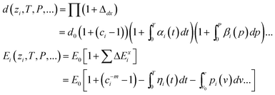
Besides the constituent elemental atoms, the key factors dominating the behavior of a substance include: (i) the interaction among atoms through charge sharing in terms of bonding, charge non-sharing or polarization in terms of nonbonding, and, (ii) the ways of configuring charge in both real and energy spaces. The core band energy shift, dominated by interatomic bond energy, provides fingerprints of what has happened to the electrons in the valence band and above as the latter provides perturbation to the Hamiltonian.
Materials can be categorized according to their atomic coordination environments: full-, heterogeneous-, tetrahedral-, and under-coordination. The full coordination system refers to the ideal elemental bulk of infinite size without any defect, edge, or impurity. Heterogeneous coordination refers to atoms associated with impurities, interfaces, alloys, compounds and artificial superlattices. Tetrahedral coordination refers to those with molecular structures like HF, H2O, NH3, and CH4 with hybridized sp orbits and the H atoms are replaced with atoms of other arbitrary elements such as metals. Under-coordination includes adatoms, defects, atomic chains, atomic sheets, grain boundaries, surfaces, and hollow or solid nanostructures in various shapes. Amorphous structures should be categorized to the under-coordinated system. A nanostructure differs from an amorphous structure in that the under-coordination is concentrated on the skin of the former but the coordination imperfection is distributed randomly in the latter. Besides the commonly known regular bonds associated with charge transportation, under-coordinated systems are always associated with coupling the quantum entrapment of energy and electrons and polarization of the lone electron, if it exists, by deeply and densely entrapped core electrons near to the under-coordinated atoms because of the shorter and stronger bonds between them.11 Tetrahedrally coordinated systems are generally associated with the coupling of lone electron pairs and lone pair-induced antibonding dipoles.12,13 Heterogeneously coordinated systems are associated with quantum entrapment or crystal potential elevation depending on the strength of the interatomic bond, of which the nature changes upon alloy and compound formation. Therefore, “coordination bond-and-band engineering” would be more efficient in dealing with the chemical and physical properties of a substance in terms of predictive design and controllable fabrication.
Very often regular bonds, broken bonds, and nonbonds coexist in one specimen. For instance, a graphite specimen contains both covalent and nonbonding π-electrons due to the sp2 orbit hybridization. The latter differentiates graphite from the bulk diamond – graphite is a conductor yet diamond is an insulator though the covalent bond in graphite is shorter (0.142 nm) and stronger (vibration wavenumber of 1553 cm−1) than those of diamond (0.154 nm, 1331 cm−1). Unrolling a single-walled carbon nanotube (SWCNT) generates a graphene nanoribbon (GNR) with the presence of huge number of broken bonds at the edges. Even such lower coordinated edge atoms substantially differentiate the GNR from otherwise rolled SWCNT or a large graphene sheet in many respects. Phenomena demonstrated by the GNR can not be seen in the SWCNT or the graphene sheet. The edge Dirac states give rise to many unusual phenomena such as the unconventional magnetism that enables carbon-only ferromagnetism, the spin glass state, spin quantum Hall effect,14–17 ultrahigh electric and thermal mobility,18,19 extremely low effective mass, and a group velocity of 1/300 times that of the light traveling in vacuum, etc. Another example is the involvement of the intermolecular lone pair interaction and the intramolecular regular bond interaction, which makes the most abundant H2O to have fascinated us for more than a century.20
Overwhelming contributions have been made in recent decades to the fabrication, characterization, and functionalization of nanostructures for technological developments. Considerable theoretical effort has also been made to the understanding of the physics and chemistry of materials at the nanoscale. It is quite often that one phenomenon induced by size is associated with numerous modeling arguments, such as the blue shift in photoluminescence,21–25 elastic enhancement,26–32 and melting point depression33–40 of nanostructures. However, mechanisms behind the bulk-unseen phenomena of the conductor–insulator transition,3 the presence of extra energy states associated with atomic vacancy,7 edge,41–43 adatoms,6 and chain ends,42,44 the extremely high catalytic ability,45 and the nonmagnetic–magnetic transition3 at the nanoscale remain poorly understood.
It is my personal view that all the intriguing property changes that emerge and their interdependence provoked by atomic under-coordination could share a common origin – interaction between the under-coordinated atoms and the associated dynamics and energetics of charge entrapment and polarization.11 In addition to charge transfer, the dynamics and energetics of the nonbond and antibond will dominate the chemical processes as they significantly re-facilitate electrons in the valence band and above. Because of the localization, inhomogeneity and energy difference between the broken bonds (0 eV), nonbonds (10−2 eV) and regular bonds (100 eV), currently available quantum or classical approximations are inadequate to describe the irregular broken bonds and nonbonds. Generally, in theoretical quantum approaches, one often employs the sum of interatomic potentials of regular bonds and their averages with great difficulty when dealing with the nonbonding weak interactions or the severe geometric and energetic relaxations caused by the broken bonds at grain boundaries. The ab initio method may derive the respective features but a clear physical picture is required for one to understand the origin of what one has derived from calculations.
In the past two decades, we have focused on: (i) the tetrahedral coordination bond-and-band formation dynamics of oxygen, nitrogen and carbon reacting with solid surfaces with the involvement of nonbonding lone pairs and antibonding dipoles;12,13 (ii) the under-coordination bonding for monatomic chains, monatomic sheets, defects, vacancies, surfaces, and nanostructures with the involvement of local bond contraction, quantum entrapment, and lone electron polarization;1 (iii) heterogeneous coordination bonding for impurities, interfaces, composites and compounds, with either interface quantum entrapment or quantum elevation and charge depletion;46 and (iv) the behavior of materials under the external stimulus of coordination, temperature, and pressure.47 Our efforts have derived preliminary theories of bond–band–barrier correlation mechanism, the bond order–length–strength (BOLS) correlation mechanism, and the local bond average approaches, which serve as the foundation of the subject of “nonbonding energetics and electronics” of this article.
Extending previous understandings,1,12,13,46,47 this work, with experimental evidence and discussions on prospective applications, aims to highlight the importance of nonbonding electrons in determining the unusual behavior of low-dimensional systems in the fields of biological, organic, and inorganic specimens. By taking examples of graphite surface vacancies, GNR and terrace edges and atomic chain end states, insulating metal clusters, defect magnetism, diamond-metal adhesion, superhardness and superelasticity of nitrides, superhydrophobicity of nano compounds, superfluidity of nanoliquids in microchannels, supersolidity in solid 4He, and superlubricity of nanocontacts, this work will discuss development and applications of theory regarding irregular nonbonding states and applications. Additionally, with the aid of the developed knowledge, we attempt to interpret some long-standing puzzles such as the high critical temperature (TC) superconductivity induced by B, C, N, O and F, the molecular structures and functionalities of NO signaling and CF4anti-coagulation in synthetic blood, as well as the density anomalies of ice.
II Regular bonds: interatomic potential and electron configuration
• Integration of the interatomic potential and wave function determines the bond energy and charge distribution.• Interatomic regular bonds and the associated charge distribution in the valence band determine the traditionally-known physical properties of a condensed specimen.
• The regular bonds define the Hamiltonian, atomic cohesive energy and related properties, including the band structure, group velocity, effective mass, melting point, mechanical strength, dielectrics, etc.
• The bonding charge follows the dispersion relationship and occupies the allowed energy states in the valance band and below.
• All detectable properties can be closely related to the nature, order, length, and energy of the bonds involved.
Covalent, ionic, and metallic bonds are the most common kinds of interatomic interaction.48 These regular bonds are realized through localised valence charge sharing by neighboring atoms in the ionic and covalently bonded systems or de-locally by all atoms of the entire body of a metal.48,49 The energies of the regular bonds are several electron volts (eV) in magnitude at equilibrium. The nearest distance between atoms or ions at equilibrium corresponds to the bond length. For example, Na interacts through a metallic bond with a cohesive energy of 1.1 eV per atom, which determines the Na to be ductile, electrically and thermally conductive. NaCl is an ideal specimen of an ionic bond with a cohesive energy of 3.28 eV atom−1, which makes NaCl harder, with a high melting point and makes it soluble in polar liquids such as water. Diamond demonstrates an ideal covalent bond with cohesive energy of 7.4 eV atom−1 and is, so far, the hardest natural material with a high melting point of 3800 K; diamond is insoluble in nearly all solvents. The polar–covalent bond, the form in between covalent and ionic bonds, exists in most alloys or compounds. The nature of the bond or the way of charge sharing in a specimen is dictated by the difference in the electronegativity of the constituent elements of the specimen.
The interatomic potentials for these stronger interactions dominate the atomic cohesive energy, the Hamiltonian and hence the band structure, dispersion relations, the allowed density-of-states (DOS) of the valence band and below, the effective mass and group velocity of charges in various bands as well. At equilibrium, the coordinates of a pairing potential correspond to the bond length and bond energy (d, Eb) that determine the binding energy density, Eb/d3. The product of the number of bonds (z) of an atom and the cohesive energy per bond is the atomic cohesive energy (zEb). All the detectable quantities of the bulk materials such as the critical temperature for crystal structural phase transition, electronic and optical properties, hardness, elasticity, melting point, are all closely related to the bond nature, order, length, and energy represented by m, z, d, Eb, respectively, or their combinations such as the cohesive energy, energy density, and lattice vibration frequency. The cohesive energy determines the thermal stability; the binding energy density determines the elasticity and mechanical strength. These regular bonds and their functionalities are well described using quantum approximations because of their periodically-ordered homogeneity and uniformity.
III Broken bonds: local bond relaxation, charge and energy entrapment
• Broken bonds lower the z value of the edge atoms, which causes the Goldschmidt–Pauling bond contraction associated with bond strength gain.• The shorter and stronger bonds provide perturbation to the local Hamiltonian, atomic cohesive energy, binding energy density and related properties.
• Structure relaxation associated with local quantum entrapment of charge and energy taking place nearby the under-coordinated atoms.
• Broken bonds dominate the size trends of bulk quantities at the nanoscale because of the local bond modification and the varied fraction of under-coordinated atoms.
• Size, temperature, and pressure coupling effect proceeds only in the surface up to skin depth.
3.1 Principle: BOLS correlation and size dependency
The broken bonds refer to the under-coordinated atoms at sites surrounding vacancies, defects, edges, surfaces and the skins of grains and cavities. Adatoms, atomic chains, atomic ribbons, and hollow tubes and spheres are also formed by under-coordinated atoms with bonds fewer than those in an ideal bulk taking the atomic CN of 12 in an fcc structure as the standard. Materials at the nanoscale can be represented by a high fraction of atoms with an effective atomic CN (or z) between the values of 0 and 12.47 The z equal to zero value corresponds to an isolated atom and z = 12 to an atom in the ideal bulk interior. These two extreme situations are unlikely happen in reality under normal circumstance. For other structures such as bcc and sc configurations, the bulk atomic CN can be normalized by the standard. The association of the proportion of such under-coordinated atoms and the strong interactions between them originates from the size dependency of materials at the nanoscale.1,47 All the detectable quantities such as the Young's modulus, dielectric constant, magnetic momentum, etc, are inversely dependant on solid size, K−1, with K being the dimensionless form of the characteristic size. It has been shown50 that the linear dependence of the detectable quantities on the inverse size is dominated by the surface skin of a limited number of atomic layers, while atoms in the core interior retain their bulk nature, making no contribution to the size dependency.The under-coordinated atoms demonstrate different kinetics of growth nucleation, atomic diffusion, and chemical reaction.51–53 The diffusion rate at these atomic sites is very high and the growth rate at these points is rather low. The chemical and thermal stability at these sites are very low. The physical properties at sites nearby under-coordinated atoms are different from those of the bulk.1,47,54
Although the broken bonds with zero energy at boundaries make no apparent contribution to the performance of materials, their impact on the ones remaining nearby is indeed profound.47 They cause the remaining bonds of the under-coordinated atoms to contract spontaneously with an associated increased in bond strength, which in turn produces localized strain and causes potential well depression with a consequence of localized densification of charge, energy and mass. The shorter and stronger bonds between under-coordinated atoms provide significant perturbation to the Hamiltonian, atomic cohesive energy, binding energy density, and associated properties when the fraction of the under-coordinated atoms is increased.
The consequence of the broken bond follows the BOLS correlation, as illustrated in Fig. 1:1,47
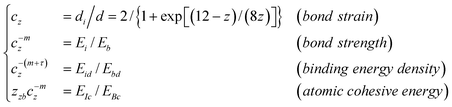 | (1) |
 | ||
| Fig. 1 (a) The BOLS correlation mechanism (solid line) formulates the atomic “CN-radius” convention of Pauling and Goldschmidt48,49 with further evidence (scattered symbols) measured from Au particles, Au–Au atomic chains and others, as discussed in the text and Ref. 1. (b) Schematic illustration of the broken-bond induced local strain and quantum entrapment at the terminating edges up to three atomic layers.55,56 | ||
| Detectable quantity Q | q (z, m, d, Eb) |
| Critical temperature Tc | ∝ zEb |
| Young's modulus Y | ∝ Ebd−3 |
| Bang gap width (EG) and core level shift E(∞)–E(1) | ∝ Eb |
| Raman optical shift (ω) (μ is the reduced mass of bonding atoms) |

|
Generally, the properties of a material change with its size in two opposite trends: one is the size-depressed properties that are related to the atomic cohesive energy, including the critical temperature of phase transition (melting, evaporation, ferro-paramagnetic, ferro-paraelectric, superconductive, etc), activation energy for atomic diffusion, frequency of atomic vibration, etc; the other is size-elevated properties relating to the bond energy such as the band structure related properties, band gap, core level shift, or binding energy density such as Young's modulus, mechanical strength, etc.1,47
One may take a specimen of any shape containing N atoms for illustration, the measurable quantity Q(∞) = Nq if no surface effect is considered, where q is the atomic scale density of the measured quantity Q. Considering the contribution from the under-coordinated atoms in the outermost three atomic layers, we can replace the Niq with Niqi in the ith atomic layer containing Ni atoms with qi representing the surface effect, which yields the following scaling relation in terms of local-bond-average approach. This relation is in consistent with the measured size dependence,
 | (2) |
3.2 Bond and band engineering
The impact of the BOLS correlation on the band gap modulation is apparent. As the band gap is proportional to the cohesive energy per bond, the gap will expand when the size of a semiconductor shrinks, such as for Si nanowires.57 For metals, the valence band will split, generating the artificial band gap, which may explain why a conductor turns to be an insulator when its size turns to be the nanoscale,3 such as Au58 and Pd59 nanostructures. The artificial band gaps for Au and Pd clusters increase with the reducing number of Au and Pd atoms in the clusters. The typical scanning tunneling spectroscopy (STS) conductive spectra for Pd and Si nanowires are compared in Fig. 2.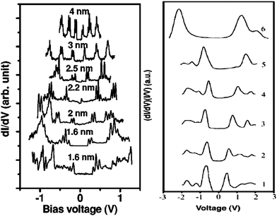 | ||
| Fig. 2 STS conductance of (a) crystalline Pd particles with diameter in the range of 1.6–4 nm59 and (b) of Si nanowires with diameters decreasing from 7 (curve 1) to 1.3 nm (curve 6)57 revealed the band gap generation in (a) and band gap expansion in (b) at the nanoscale. | ||
Without igniting electron–phonon interaction at T = 4 K or electron-hole production or combination, the vehicle for the quantum confinement theory, STS revealed that the EG of Si nanorods increases from 1.1 eV to 3.5 eV when the wire diameter is reduced from 7.0 to 1.3 nm and that the surface Si–Si bond contracts by ∼12% from the bulk value (0.263 nm) to ∼0.23 nm.57 This finding concurs excitingly with the BOLS expectation: CN imperfection shortens and strengthens the remaining bonds of the lower-coordinated atoms associated with EG expansion that is proportional to the single bond energy. Similarly, the size-enlarged EG of Si nanorods, Si nanodots, Ge nanostructures, and other III–V and II–VI semiconductors at the nanoscale follows closely the BOLS prediction without involving electron-hole interaction, electron–phonon coupling or quantum confinement.1,60,61
3.3 BOLS-enhanced capability of available techniques
It is worth noting that the new degrees-of-freedom of size not only allows us to tune the physical properties of a specimen but also provides us with opportunities to gain the conventionally unavailable information such as the core level energy of an isolated atom and its shift upon bulk formation,62 the frequency of dimer vibration and its shift upon bulk formation,47,63 for instance, by combing the BOLS theory and the measured size dependence of X-ray photoelectron spectroscopy (XPS) and Raman spectroscopy.Here we just show the XPS results for illustration. The principles for deriving such information are very simple. The core-level energy shift from that of an isolated atom is dominated by the crystal potential in the Hamiltonian. The eigen wavefunctions, φν(r), for the core electrons remain unperturbed by coordination reduction as these electrons are strongly localized. ν is the quantum number for a specific energy band. Any perturbation in the Hamiltonian of an extended bulk solid will lead the core level to shift further from that of the bulk. The direction of the shift depends on the perturbation to the potential. The perturbation includes bond contraction, bond nature alteration, charge polarization, and other external stimuli. As the crystal potential at equilibrium corresponds to bond length and bond energy; the core level shift is proportional to the bond energy.
Analytically, the core level shift of a surface and a nanostructure of K size can be formulated by the combination of band theory64 and the BOLS correlation.62 The single-body Hamiltonian is perturbed by the shorter and stronger bonds, denoted with ΔH:
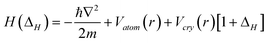
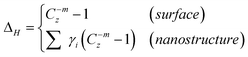 | (3) |
Where α = −〈φν(r)|Vcryst(r)|φν(r)〉 and β = −〈φν(r)|Vcryst(r)|φν(r − d)〉 are the exchange and overlap integrals; β/α ≈ 1/100 and 〈φν(r)|φν(r − d)〉 = 0; 〈φν(r)|φν(r)〉 = 1 because of the localized nature of the eigen wavefunction for electrons in the core shells.65
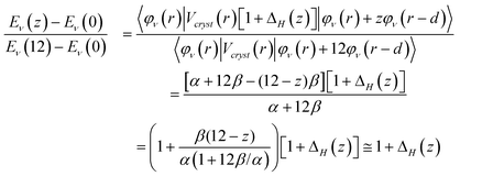
Therefore, we have a general form for the size and surface induced core level shift:
 | (4) |
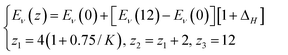
As illustrated in Fig. 3, the upper part is a typical XPS spectrum that is broken down into components representing contributions from different surface shells and the bulk with each component an effective atomic CN. If the solid size is reduced, the spectral intensities of the surface and defect components will increase with the fraction of such under-coordinated surface and defect atoms rendering the intensity of the bulk component in the XPS. When the solid size is increased from one atom, the energy level shifts from the Eν(0) to Eν(z) until a maximum of the unit cell size (K = 1.5, or z = 2) and then reverses up to the bulk value of Eν(12), as illustrated in the lower part of Fig. 3.
![Atomic CN-resolved core level shift.69 The energy of the quantum entrapment perturbs the Hamiltonian that determines the binding energy (BE) shift from that of an isolated atom, Eν(z) − Eν(0), which is proportional to the bond energy at equilibrium: [Eν(z) − Eν(0)]/[Eν(12) − Eν(0)] = Ei : Eb = C−mi. S1(z = 4) and S2(z = 6) represent the fist and the second surface layers and B (z = 12) the bulk component. Sdefect (z = 2, 3) represents the contribution from adatoms or edges atoms. The energy of the convoluted envelope changes with solid size because of the variation in surface-to-volume ratio.](/image/article/2010/NR/c0nr00245c/c0nr00245c-f3.gif) | ||
Fig. 3 Atomic CN-resolved core level shift.69 The energy of the quantum entrapment perturbs the Hamiltonian that determines the binding energy (BE) shift from that of an isolated atom, Eν(z) − Eν(0), which is proportional to the bond energy at equilibrium: [Eν(z) − Eν(0)]/[Eν(12) − Eν(0)] = Ei![[thin space (1/6-em)]](https://www.rsc.org/images/entities/char_2009.gif) :Eb = C−mi. S1(z = 4) and S2(z = 6) represent the fist and the second surface layers and B (z = 12) the bulk component. Sdefect (z = 2, 3) represents the contribution from adatoms or edges atoms. The energy of the convoluted envelope changes with solid size because of the variation in surface-to-volume ratio. :Eb = C−mi. S1(z = 4) and S2(z = 6) represent the fist and the second surface layers and B (z = 12) the bulk component. Sdefect (z = 2, 3) represents the contribution from adatoms or edges atoms. The energy of the convoluted envelope changes with solid size because of the variation in surface-to-volume ratio. | ||
By integrating BOLS theory with the XPS technique, one can readily determine the Eν(0) value and its bulk shift ΔEν(12) = Eν(12) − Eν(0), as listed in Table 2, by matching the prediction to the measured size dependence of ΔEν(K) = Eν(K) − Eν(0) or decomposing the XPS profile from a surface. Combining XPS, Auger spectroscopy and BOLS theory, we can also obtain additional information regarding the coefficients of screening and charge transport in a reaction.66
3.4 Unification of defects, surfaces, and nanostructures
Defects, surfaces, and nanostructures of various shapes are correlated by atomic under-coordination. The interaction between the under-coordinated atoms and the nearby charge distribution is the origin of the unusual performance of such under-coordinated systems. The broken bonds-induced strain and bond energy gain results in excessive energy on the surface of skin depth, and therefore, a surface exhibits higher stress and tension than those in the bulk interior. The surface energy, stress and tension determine the processes and phenomena at a solid or liquid surface including structural reconstruction, relaxation, adhesion, reaction and friction. A solid surface is often harder and more elastic than the bulk interior but the surface melts easier. On the other hand, the cohesive energy of an under-coordinated surface atom is generally lower than that of the bulk. Therefore, surface and defect atoms are chemically and thermally less stable.The longstanding confusion about surface energetics and their dimension units can thus be clarified as:70 (i) the energy density gain (in unit of eV nm−3) in the surface skin consisting of two interatomic spacings, (ii) the residual cohesive energy of the discrete surface atoms (eV atom−1), and (iii) the energy per unit area (eV nm−2) required for cutting one body into two parts. Term (i) is related to the elastic modulus and mechanical strength, as well as the electroaffinity, and term (ii) to the thermodynamic activities such as activation of dislocation motion, diffusion and phase transition. This classification clarifies why a surface is harder yet melts easier, and why a surface atom is thermally and chemically less stable. The defect serves not only as the center that initiates mechanical failure but also sites of energy entrapment, between which the competition determines the strength of materials at the nanoscale.71
Knowledge of the surface energetics can also be applied to bonds at the inner surfaces of nanocavities,72 which helps one to understand why foams composed of nanometre-sized pores are lighter but stronger, and why they are chemically and thermally less stable. These properties add advantages to the porous foams that can be used in impact energy management, catalysis and sensors, as well as hydrogen storage and drug delivery.
With a given form of interatomic potential, u(r), one can derive the analytical expressions for the elastic modulus and the stress at the ith atomic site:
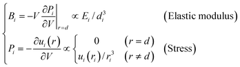 | (5) |
Bond contraction turns the skin of a liquid drop to a structurally ordered, solid-like, and elastic covering sheet.73–75 Normally, a solid skin melts first, yet a liquid skin solidifies prior to the liquid interior because of the lowered critical temperature for liquid–solid phase transition at the surface. This finding offers an understanding of the formation mechanism for gas bubbles and liquid drops as well as the origin of surface tension of a liquid. It has been found that bonds surrounding atomic impurities also contract with an association of locally bounded states (entrapment as well).76 These findings suggest that the excessive interface energy arises from the bond deformation and bond nature alteration at a compacted interface. Surfaces, defects, and nanostructures are thus correlated by the atomic under-coordination and the subsequent bond contraction.
3.5 Coordination, temperature, and pressure coupling
Since the works of Alivisatos and co-workers,77,78 there has been a huge database showing consistently that the critical pressure (PC) for the transition from the less-coordinated structural phase to the denser structures increases with the reduction of crystal size. For the bulk CdSe, the transition pressure is 2.5 GPa but when the size is reduced to 1–3 nanometres across, the transition pressure increases to a value of 5 GPa. The size trend for the pressure-induced γ-Fe2O3 (maghemite) to α-Fe2O3 (haematite) transition showed that 7 nm nanocrystals transform at 27 GPa, 5 nm ones at 34 GPa, and 3 nm ones at 37 GPa.78Fig. 4a shows the typical V–P profiles79 measured at the ambient temperature for SnO2 bulk and powders of 14, 8, and 3 nm across. The critical pressures for phase transition change with both K and P. The PC is higher for the smaller solid. The slope of the V–P profile, β = dV/(V0dp), corresponds to bulk compressibility. Although the pressure-induced TC enhancement has been intensively investigated, factors controlling the size trend of the pressure-induced phase transition in nanocrystals and theoretically reproduction of the observed trends have long been difficult challenges. The coupling of solid size, temperature, and pressure has led to new phenomena requiring clear understanding.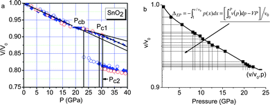 | ||
| Fig. 4 (a) The V–P profile for SnO2 nanocrystals phase transition from rutile to cubic structures.79 The square, diamond, circle and up-triangle symbols represent bulk, 14 nm, 8 nm, and 3 nm SnO2 samples, respectively. Corresponding critical transition pressures are denoted as PCb, PC1, and PC2, while PC3 for the 3 nm crystal is beyond the measured pressure range. (b) Schematic illustration of the pressure-enhanced bond energy and volume compression. The integration of the V–P profile represents energy stored in the crystal to raise the TC for phase transition, under the conditions of bond number conservation.80 | ||
If the nanostructure is under externally applied pressure and temperature, only the parameters of d and Ei among (m, z, d, Ei) can be changed before phase transition. The coupling effect on the bond length and bond energy can be expressed as,
 | (6) |
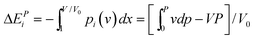 | (7) |
The joint effect of multiple fields on the cohesive energy of nanocrystals can be integrated based on the rule of energy superposition. These external stimuli provide perturbations in the crystal cohesive energy, in a similar way to the effect of bond order loss,63 based on the core-shell configuration,
 | (8) |
 | (9) |
The first part represents purely the effect of size and the second part the joint effect of other stimuli. The effect of multi-filed coupling proceeds only in the surface up to skin depth, as seen from the 2nd part of the 2nd term.
From eqn (9), we can obtain the KC, TC, and PC dependence of the solid–solid phase transition at the nanoscale,
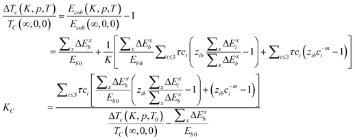 | (10) |
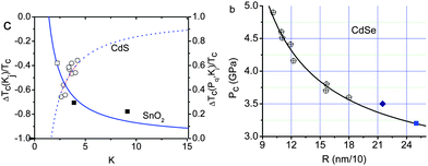 | ||
| Fig. 5 (a) Comparison of the predicted (solid curves) with the measured (scattered symbols) pressure-induced TC elevation for solid–solid transition of SnO2 nanocrystals derived from Fig. 4b and the size-induced TC depression for solid–liquid transition of CdS nanocrystals, showing compensation of the relative changes.82 The empty square is an extrapolation of the 3 nm SnO2 solid, the transition pressure of which is predicted to be 43 GPa. (b) Theoretical reproduction of the size and pressure dependence of the phase transition of CdSe nanocrystals at room temperature (ΔTC = 0).81,82 | ||
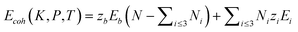
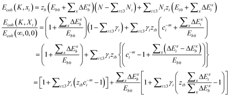
IV Nonbonding interactions associated with tetrahedral coordination
• Nonbonding interactions with energies similar to that of the body temperature and a vibration frequency in the tera-Hz regime contribute insignificantly to the Hamiltonian or atomic cohesive energy.• However, these nonbonding electrons add impurity states near to EF, which neither follow the standard dispersion nor occupy the allowed energy states.
• The coupling of lone electron pairs and the lone pair-induced dipoles due to sp orbit hybridization plays an important role in the functions of biological, organic, and inorganic compound electronics.
• Most importantly, the lone pair can modulate interface stress and facilitate self-lubrication with high elasticity under the critical load.
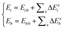
• In the hydrogen and hydrogen-like bond, the shorter intramolecular bond and the longer intermolecular nonbond change their lengths and energies oppositely and simultaneously.
4.1 Principle: lone pair and dipole creation
Nonbonding and antibonding interactions are associated with the reaction process of tetrahedrally-coordinated bond formation.12,13 In addition to the process of charge transportation from donors to the electronegative acceptors, sp orbit hybridization, charge localization and polarization take place. The “nonbonding” states refer to the energetic electrons involved in the nonbonding lone pairs, antibonding dipoles, as well as H-like and C–H-like bonds. An ionic impurity in a metal will also induce dipoles.13,83 The Van der Waals bond, having a maximal energy of several tenths of an eV, should be in this category as it represents dipole–dipole interaction instead of charge sharing. CH4 is a typical case of intermolecular Van der Waals bonds and intramolecular C–H covalent bonds with intermolecular cohesive energy of 0.1 eV atom−1. The weak intermolecular interaction makes the CH4 soft, with a low melting point and soluble in covalent liquids.The weak interactions contribute insignificantly to the Hamiltonian or the atomic cohesive energy. These electrons, however, add impurity states in the vicinity of the Fermi energy, which neither follow the regular dispersion relations nor occupy the allowed states of the valence band and below. They are located in the correct energy scope for STM/S. The lone pair and dipole interactions not only act as the most important function groups in biological and organic molecules but also play an important role in inorganic compounds.
Nonbonding lone pairs and antibonding dipoles are generated in a reaction with sp3 orbit hybridization being involved, such as in the processes of,
| NH3 → 3H+–N3− (:Hp) |
| H2O → 2H+–O2− (:2Hp) |
| HF → H+–F− (:3Hp) |
A typical H2O and NH3 molecule and the charge density modification in the valence band and above are illustrated in Fig. 6. The sp3 orbit hybridization in the electronegative atoms produces four directional orbits, each capable of being occupied by two electrons, forming a quasi-tetrahedron. These four directional orbits can hence support the occupancy of eight electrons. The central O atom, for example, has six 2s22p4 electrons and requires another two to complete its valence shell. Therefore, the O forms two bonds with its nearest neighbors by taking one electron from each to share the orbits, while its remaining two orbits are occupied by the lone electron pairs of the O. Likewise, a nitrogen atom needs three electrons for sharing and generates one lone pair. Similarly, a F atom forms a tetrahedron with three lone pairs. In additional to the weak interactions with energies of ∼50 meV, as detected using Raman and electron energy loss spectroscopy (EELS),13 these lone pairs polarize the neighbouring atoms instead causing their change to dipoles. Strikingly, the manner of electronic distribution, bond type, bond length and bond energy surrounding the central O or N atom in the tetrahedron are all anisotropic.
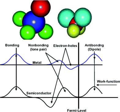 | ||
| Fig. 6 (a) NH3 and (b) H2O molecule and (c) the corresponding modification of the valence DOS for metals and semiconductors with four excessive DOS features: bonding (≪ EF), lone pairs (< EF), electron holes (< EF), and dipoles (> EF). The three DOS features closing to the EF are often overlooked yet they are crucial to the performance of a compound. | ||
Counting from lower to higher binding energy (Fig. 6c), the DOS features are the bonding state (O2− or N3−), electronic holes (H+), lone pair electrons (:) and dipoles (Hp). Such a valence DOS structure is also applicable in describing molecules similar to HF with three lone pairs being involved. In semiconductor compounds, hole formation occurs at the upper edge of the valence band, which expands the semiconductor's band gap further, turning a semiconductor into an insulator. In metallic compounds, the holes are produced at the Fermi surface, hence causing the formation of a band gap. This is the reason for the metallic compound's loss of conductivity to become either a semiconductor or an insulator. Nonbonding states are situated in the band gap to form impurity states close to Fermi surface, while antibonding states are situated above the Fermi energy. The production of dipoles will shift the surface potential barrier outwardly with high saturation,84 opposing to the effect of the charged ions. The former can be observed using STM as protrusions, while the latter depressions. The orientation of such a tetrahedron in a bulk is also subject to its coordination environment.85 The difference between N, O and F is in the structural symmetry and the number of lone pairs in one tetrahedron.
4.2 Cu3C2H2 and Cu3O2 on the Cu(001) surface
Fig. 7 shows how the dipoles are generated in the processes of chemical reactions and how these reactions can be formulated with identification of the valence state of an individual atom. The STM images and the corresponding bond configurations are shown for the C2H2 molecule chemisorption on Cu(001) (1 × 1) surface83 and the O-induced Cu(001) (2 × 2√2) R45° surface reconstruction.13 The Cu3C2H2 molecular configuration was optimized using density function theory (DFT) calculations86 and the Cu3O2 bond structure was determined by very-low-energy electron diffraction (VLEED) calculations.87 These chemical reactions can be formulated with identification of individual atomic valences as follows: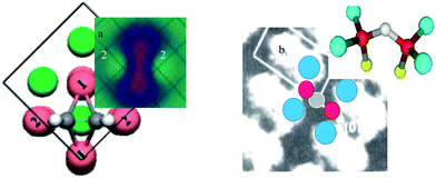 | ||
| Fig. 7 STM images and the corresponding bond configurations for (a) Cu3C2H2 and (b) Cu3O2 on the Cu(001) surface.13,83,88 The bright protrusions are dipoles induced by H+ in (a) (labeled 2) and by the lone electron pairs of oxygen in (b) while the depressions are ions (see text for equations formulating the reaction dynamics and individual atomic valances). | ||
For the C2H2–Cu(100) (1 × 1) surface reaction:
| C2H2 + 4Cu (surface) + Cu (substrate) ⇒ 2C4− (hybrid) + 2H+ + 2Cu2+ (surface) + Cu2+ (substrate) + 2Cup(H+induced, labeled 2) |
For the O2–Cu(100) (2 × 2√2) R45°surface reaction:
| O2 + 4Cu (surface) + 2Cu (substrate) ⇒ 2O2− (hybrid) + Cu2+ (surface) + 2Cu+ (substrate) + 2Cup(lone pair induced) + Cu (missing vacancy) |
The high protrusions in the STM images correspond to the Cup dipole states induced either by H+ in (a) or by the lone electron pairs of oxygen in (b) but the depressions to the Cu2+ and O2− ionic states in both cases. The “dumbbell” shaped depression in (a) is the Cu2+ and C4− states; the “dumbbell” shaped protrusions in (b) are the Cup ↔ Cup pairing dipoles crossing over a raw of missing Cu atomic vacancies in the surface layer.87 The “dumbbell” pairing dipoles interact through Van der Waals repulsion force. STS measurement from the Cup:O2−:Cup chain at the O–Cu(110) surface89 revealed that the lone pair states are located at −2.1 eV below EF and the dipole states extend in the range of 0.5–2.0 eV above EF.13 Quantitative analysis using the combination of STM88,90 and VLEED84,87 revealed that the Cu3O2 pairing-tetrahedron forms in four discrete stages while the O turns from the O1− to the O2− state. It has also been found that the O2−:Cup nonbonding part expands while the Cu+–O2− bond contracts at the surface, which may provide an explanation of the anomalous phenomena of the NTE of ice and spin ice glasses volume contraction up heating.
It has also been found using XRD and extended X-ray absorption fine structure (EXAFS) measurements91 that Cu2O and Ag2O exhibit a NTE of the lattice parameter over extended temperature intervals (from 9 to 240 K for Cu2O, up to 470 K for Ag2O) and anisotropic thermal displacements of M atoms (M = Cu, Ag). EXAFS measures a positive expansion of the nearest-neighbors M–O pair distance and a perpendicular to parallel anisotropy of relative motion, much stronger than the anisotropy of the absolute M motion. The M–O bond is much stiffer towards stretching than bending. According to the EXAFS data, out of the 12 M–M next-nearest-neighbor pairs, the 6 connected via a bridging oxygen undergo negative expansion, while the 6 lacking the bridging oxygen undergo positive expansion. These results show a rather complex local behavior, which, while confirming the connection of NTE to O–Cu–O bonding, is in consistent with our VLEED findings at the O–Cu(001) surface.
The impact of the nonbonding lone pairs and the antibonding dipoles is abundant. For example, the presence of antibonding dipoles lowers the work functions drastically by more than 1 eV,92 which greatly aids electron emission for imaging and display.93–95 The nitrogenation of diamond and carbon nanotubes, the oxidation and fluorination of metals, etc., have all been widely used in industrial sectors. It is expected that proper doping of N, O and F to the surface of low workfunction metals could be beneficial to the field emission.92
4.3 Interface stress neutralization and metal–nonmetal joining
It has been discovered96 that N chemisorption generates tensile bond stress while C chemisorption results in compressive bonds at the Ni(100) surface from the STM images of the adsorbate-induced “clock and anticlock” reconstructions. The presence of only one lone pair of N makes a great difference in the surface stress. These findings would help in designing processes and functional materials for practical applications at an interface.It becomes clear from the above analysis96 that carbon-induced compressive stress prevents diamond from being grown adhesively to metal substrate – a long standing challenge for industrial applications. However, thanks to the lone pair of nitrogen that could alternate the situation by giving rise to the tension, it is possible to neutralize the interfacial stress between diamond and a metallic substrate by integrating a graded TiCN buffer layer into designs.96 In this exercise, we introduced nitrogen in the vacuum chamber of film deposition using microwave-enhanced plasma CVD with an Ar–CH4 gas mixture and then gradually reduced the partial pressure of nitrogen down to zero. The film is then grown very firmly on metals. Mechanical tests confirmed the desired high adhesion, verifying the design and the associated modeling considerations. The use of such a graded buffer layer to neutralize interfacial stresses can also be extended for use in other nonmetal–metal joining applications in order to improve their interfacial strengths.
4.4 Lone pair induced tera-Hz lattice dynamics, self-lubrication, and superelasticity
We can also design artificial crystals based on such a bond structure configuration: the intra-layer bonds are mainly ionic or covalent, while the interlayer is dominated by the relatively weaker lone pairs. This structure is similar but not entirely the same to that of graphite, whose inter-layer is dominated by Van der Wales π-bond interactions. The design of this structure imparts a low frictional, and hence greatly lubricating, nature with high hardness below a critical load. Fig. 8a compares the measured hardness and elasticity of a GaAlN film97versus amorphous carbon.98 Strikingly, the nitride is harder and more elastic with a 100% elastic recovery opposed to the latter. The latter is often harder than the former in real high-load applications. Experimental results also showed that the coefficient of friction for the nitride is much lower than that of amorphous carbon or diamond. However, as the applied load increased past a critical value (μN level), the coefficient of friction increased drastically, indicating the failure of the weaker nonbonding interactions, as we have expected.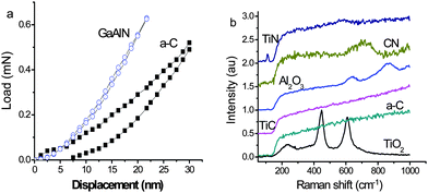 | ||
| Fig. 8 Comparison of (a) the hardness and elastic recovery of GaAlN with that of amorphous carbon and (b) the Raman frequency shifts of oxides, nitrides, and carbides. The carbides show no lone pair vibration features at low frequencies.98 | ||
Fig. 8b compares the nonbonding vibration features detected using Raman spectroscopy for randomly selected oxides, nitrides, and carbides. The results clearly show the expected tera-Hz (f = 1012 = cν = 3 × 10⁸ × ν, with ν being the wavenumber limited to 30–350 cm−1 and vibration energy of 4–45 meV) low-frequency vibrations in oxides and nitrides with an intensity that is proportional to the number of the lone pairs in one tetrahedron. The peak frequency is determined by the force constant and the reduced mass of the pairing atoms, (k/μ)1/2, via nonbonding interactions. For an oxide tetrahedron, there are two lone pairs while for a nitride there is one. None are present in the carbide tetrahedron. These results are evidence of the essentiality of tetrahedral bond formation with discrimination of the presence of lone pairs to N and O.
From the observations, we may clarify that surface enhanced Raman spectroscopy (SERS) in the tera-Hz range corresponds to the resonance of lone pair vibration of biological molecules adsorbed on rough metal surfaces. The high enhancement SERS factor of 1014–1015 allows the technique to be sensitive enough to detect single molecules. Such order of phonon vibrations also exist in the ZrWO8 NTE specimen.99
V Nonbonding interactions associated with under-coordination
• Associated with atomic under-coordination, nonbonding lone electrons are strongly and locally polarized by the deeply and densely entrapped core and bonding electrons that follow the rule of BOLS.• Similar to the lone pairs and dipoles, the polarized lone electrons follow neither the dispersion relationships nor occupy the allowed states in the valence band and below but they generate the midgap impurity states in the vicinity of Fermi energy.
• Coupling of the entrapment and the polarization originates properties that bulk materials do not demonstrate.
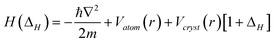
5.1 Principle: Nonbonding electron polarization by quantum entrapment
At the terminating end of a solid, the characteristics of the nonbonding lone-electron states become even more pronounced. Polarization occurs to the lone electrons, if they exist, by the densely trapped bonding and core electrons of the under-coordinated atoms, as illustrated in Fig. 9. As a consequence of the shorter and stronger bonds and the polarization screening effect, denoted with ΔH, the single-body Hamiltonian turns to be:where
 | (11) |
 | ||
| Fig. 9 Schematic illustration of the atomic under-coordination induced local bond contraction (di < d0), the associated quantum entrapment (T) and the polarization of the nonbonding states (P) by the densely entrapped bonding and core charges. This sequence of processes modulates the Hamiltonian by crystal potential splitting and charge distribution in all bands. | ||
The following phenomena are expected to happen due to the coupling of the local bond relaxation, quantum entrapment, and lone electron polarization:
(i) The locally locked lone electron dipoles will form at sites surrounding atomic vacancies, defects, adatoms, GNR edges, atomic chain ends, terrace edges, etc.
(ii) The dipole states are readily probed using STM/S as high protrusions with energies near to EF.
(iii) The quantum entrapment and polarization will split the crystal potential that can be readily resolved using a newly developed photoelectron residual spectroscopy (PRS) technique.
(iv) Valence band splitting is expected to be responsible for the conductor–insulator transition and the origin for the tunable surface and nanostructure plasma resonance.
(v) The polarized lone electrons demonstrate non-zero spin values responsible for the measured magnetism in the graphene edge,9 graphite atomic vacancy,7 monolayer terrace edge100 or graphene ribbon edge101 terrace edge7 and nonmagnetic metal clusters,102 but their stability and intensity are subject to confirmation for practical device applications.
(vi) Coulomb repulsion at the contact interfaces would be responsible for the superhydrophobicity, superlubricity, superfluidity and supersolidity.103
5.2 End and edge states: STM/S and PRS
 | ||
| Fig. 10 STM/S probed (a) Au–Au atomic chains, (b) the additional end states at −0.7 eV, (c) the apparent dimensional and (d) the line scan difference between the end and the chain interior atoms.42 | ||
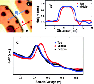 | ||
| Fig. 11 STM image104 (a) of a Au nanowire and (b) the line scans crossing the wire at the top, middle and bottom sites and (c) the dI/dV spectra recorded at the three different locations demonstrates the width effect on the polarization of the occupied LDOS. | ||
Although the STM/S has revealed the common feature of the protrusions and the states at the edges, their physical origin remains puzzling. In order to clarify the physical origin for the observed polarization and to verify the BOLS prediction, we conducted DFT calculations of the well-defined cuboctahedral (CO-13, 55, 147) and Marks decahedral (MD-13, 49,75) gold clusters.11 The resultant LDOS of the MD and CO clusters in Fig. 12 demonstrates the size dependence of charge polarization.
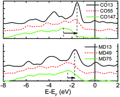 | ||
| Fig. 12 The size-resolved valence LDOS of Au–MD and Au–CO clusters shows that as the number of atoms is reduced the LDOS moves up towards EF (positioned at 0). The polarization trend agrees with the STM/S observations of gold islands of different sizes104 and from the gold monatomic chain.42 The DOS of the smallest island moves up the most and the polarization is most significant at the chain end. | ||
DFT calculations confirmed the BOLS expected lattice strain, charge transfer in real space from the inner to the outer atomic shells, valence charge polarization from lower to higher binding energies of the well-defined gold clusters. Bonds between the less coordinated atoms at corners or edges contract more significantly than those in the cluster interior. The Au–Au distance contracts up to 30%, in line with experimental observations of the Au cluster55 and Au–Au chain bonds.105 Meanwhile, the charge flows from the inner shell to the outermost of the clusters by an amount up to 1.5 electrons per atom, which agrees with the STM/S measurement from Au–Au chains deposited on NiAl(110) surface;44 chains containing three to seven Au atoms are found to host up to three extra electrons. Furthermore, under-coordination induced potential well depression and the size dependent Au 4f core level shift62 are also in line with the mean inner potential well depression detected using transmission electron microscopy.106
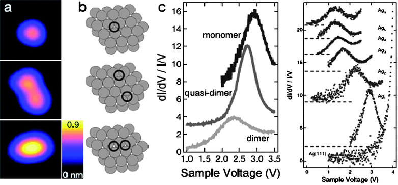 | ||
| Fig. 13 STM/S profiles of (a) the under-coordination effect on the polarization of the unoccupied state of (b) a Ag monomer, Ag quasi-dimer and Ag2 dimer under positive bias.107 The unoccupied states (c) for the monomer, quasi-dimer, and dimer are located at 3.0, 2.7 and 2.4 eV, respectively. (d) Normalized STS spectra acquired from clean Ag(111) surface and Agn (n = 1–5, 10) clusters. The dashed lines indicate the respective zero of the spectra.108 | ||
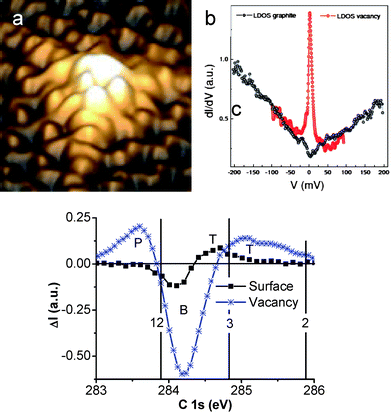 | ||
| Fig. 14 STM images of (a) the graphite surface vacancy7 showing high protrusions associated with (b) the Dirac resonant states nearby EF. The surface without vacancies shows no such states. (c) Purified graphite surface and vacancy C 1s states with extra P and T states due to variation of atomic CNs. | ||
The STM/S finding of graphite surface and vacancy states is indeed exciting. However, clarification of the nature and origin of the observation remains challenging. Therefore, gaining statistical information about bonds and electrons in the valence band and below and localized in the atomic-scaled zones, beside that provided by STM/S, is very important but so far it is by no means possible. Such information gained from sources other than STM/S is greatly needed not only for a better understanding of the vacancy states but also for materials design and processes control.
Recent theoretical109 and experimental110 investigations revealed that gold atoms attached to single vacancies near the edges of GNR tend to be on top of the vacancy, as in an infinite graphene sheet. Energy of 5 eV is needed for the Au atom to move through the vacancy to the other side of the sheet, but the Au atom can migrate in a lateral direction together with the vacancy, with a migration barrier of about 2.2 eV. The sites near the edges of the GNR are energetically more favorable for gold atom vacancy pairs than sites in the middle of extended graphene layers. The migration barriers for different pathways show that it is easier for the gold atom to move towards the edge where it can be captured. When the gold atom reaches the edge, it can migrate along the edge with an energy barrier of only 1.4 eV. The lowered barrier of Au atom migration along the edge provides further evidence for polarization without charge transition between the Au and carbon being likely. Using DFT and TB methods, Krasheninnikov et al.111 found that the mechanism of single vacancy migration in nanotubes is different from that in graphite, as the curvature of the nanotube atomic network breaks the trigonal symmetry of a perfect graphene sheet, making the diffusion anisotropic, and strongly influencing the migration barrier.112 They further demonstrated that the formation energy of a double vacancy in nanotubes is smaller than that for a single vacancy, a behavior different from most monatomic solids, including graphite. The defects also affect the elastic modulus of CNT113 as vacancies serve as not only the centers of mechanical failure but also sites of energy trapping.47
Driven by our increased knowledge and in the particular STM/S findings,7,8 we have developed a unique method of photoelectron residual spectroscopy (PRS) that has enabled us to purify the bond and electronic information within the atomic-scaled selected zones surrounding defect, surface, subsurface, and bulk by altering measurement conditions and surface treatments and combining the collected spectra according to need. With this method, we have studied a number of under-coordinated systems including Rh and Pt adatoms,6 CuPd and AgPd interfaces,46 graphite surface with and without atomic vacancies that were generated by a spray of energetic Ar+ ions.114
BOLS reproduction115,116 of the elastic modulus117,118 and the melting point119 of carbon nanotubes, and the C 1s core level shift of carbon allotropes68,120 has revealed that the C–C bond between two-coordinated atoms contracts by 30% from 0.154 nm to 0.107 nm and the bond energy increases by 150% with respect to those of diamond, giving an optimized bond nature indicator of m = 2.56 for carbon. Meanwhile, we have been able to determine the energy level of an isolated C atom, E1s(0) = 282.57 eV, and its bulk diamond shift, E1s(12) − E1s(0) = 1.32 eV, and the following z-dependence of the C 1s energy shift that is used to calibrate the XPS spectral components:68
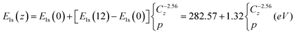 | (12) |
This relation allows us to specify the effective atomic CN of the PRS components. Fig. 14c shows the PRS purified C 1s DOS from graphite surface with and without vacancies. Results show clearly that at the clean surface, only quantum trapping states (T) are present while the atomic vacancy generates the extra polarized states. The effective atomic CN of the graphite surface skin is centered at ∼3.2 and for the vacancy neighbors is at ∼2.5. A drop in one CN makes a huge difference in the electronic structure. The vacancy induced P states are centered at 283.63 eV, or 0.31 eV above that (283.94 eV) of bulk diamond. Therefore, p = (283.63−282.57)/1.32 = 1.06/1.32 = 0.80, which means that screened potential is 20% shallower than that in diamond, while the vacancy trapping potential is C−2.56z = 2.5 − 1 = 0.97 times deeper. At the surface, the C–C bond contracts by C−13.2= −17% and the skin quantum trap depression by C−2.563.2 = 1.61 = (287.7−282.57)/1.32 folds that of the bulk potential.
PRS findings confirm the BOLS prediction and clarify that the atomic under-coordination induces local strain and quantum entrapment (T) of core charge and energy; the densely and deeply trapped charges polarize in turn the other π-electrons and the dangling σ-bond electrons, leading to the STM/S mapped protrusions and the Dirac resonant EF states,7 which, in turn, partially screens and splits the crystal potential, giving rise to the P states in the XPS C 1s profile. Therefore, the STM/S and PRS are correlated, providing more comprehensive information than using STM/S alone.
The experimental discovery10 that the minimal energy (7.5 eV/bond) required for breaking a 2-coordinated carbon atom near a vacancy is 32% higher than that (5.67 eV/bond) required for breaking a 3-coordinated carbon atom in graphene provides direct evidence for the BOLS prediction that the broken bonds do enhance the neighboring bond strength. The findings of bond contraction of gold cluster surface layers,55 Nb,121 Ta,122 and Mo123 surfaces also conform the BOLS expectation.
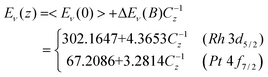
Typical PRS spectra are compared in Fig. 15. As expected, the BOLS anticipated global quantum entrapment occurs at both Pt(5d106s0) and Rh(4d85s1) adatoms. Polarization does happen, only to the otherwise conducting s-electrons of Rh. In addition to the trapped states at energies of z = 4 and 6, the original trapped states centered at z = 3 disappear with an addition of the polarized P states centered at 306.20 eV, above the bulk component, B, or the spectral valley. The valley at 307.25 eV comes from the effect of polarization-entrapment coupling. The polarization screens the crystal potential and hence the polarization and quantum entrapment split the crystal potential. Meanwhile, the polarization also screens the trapped component, and then the second valley is generated at the lower end of the spectrum. This sequence of processes is exactly the same as that of the graphite vacancy or graphene edge atoms.
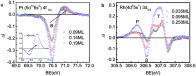 | ||
| Fig. 15 The PRS spectra6 due to (a) Pt(6s0) and (b) Rh(5s1) adatoms (coverage in ML) revealed that the Pt adatom serves as an acceptor while Rh adatom as a donor in catalytic reactions because of the broken bond-induced local strain and quantum entrapment (T) for both Rh and Pt, and the s-electron polarization (P) for Rh only. The valley B corresponds to the bulk component while the valley at 307.25 eV for Rh arises from the coupling of quantum entrapment and polarization. The inset in (a) is the PRS for the hexagonally reconstructed Pt(001) surface with denser edges,125 exhibiting the same features as that of Pt adatoms. | ||
It is seen that the extent of entrapment and polarization increases with adatom coverage up to 0.25 ML. The spectral difference between Pt and Rh coincides exceedingly well with the BOLS expectation that only the otherwise conductive half-filled s-electron of Rh adatoms can be polarized and locked as dipoles, no longer making a contribution to the conductivity. These polarized s-electrons are suggested to be responsible for the magnetism of the small clusters as well.1,129 It is important to note that the adatom or defect states may include one or two components. One corresponds to the global quantum entrapment in the lower energy and the other polarization of the otherwise conducting lone electrons. The presence of the polarization is subject to the electronic configuration in the top edge of the valence band of the specimen. The coupling of the entrapment and polarization may create a valley in the deeper band tail, see b, causes a negative shift of the entire core band.
We have also examined the Pt 4f7/2 PRS of the hexagonally reconstructed Pt(100) surface with denser edges,125 as shown in the Fig. 15a inset. The PRS displays the same quantum entrapment nature as those demonstrated by Pt adatoms. Due to a contraction of the Pt–Pt distance, the reconstructed Pt(100) topmost layer accommodates about 25% more atoms than the ideal (100) layer. This finding further supports the BOLS derivatives regarding the structural relaxation and quantum entrapment by the shorter and stronger bonds between under-coordinated atoms.
It is suggested that the quantum entrapment increases both the electroaffinity and the work function but the polarization does oppositely. Therefore, the Rh adatom is identified as a donor and Pt as an acceptor in the catalytic reactions. It is clear now why the under-coordinated atoms of the two elements are functioning differently in the processes of NO and CO oxidation and hydrogenation. This approach has also been applied to the Cu/Pd and Ag/Pd nanoalloys revealing that the Cu/Pd serves as an accepter but Ag/Pd as donor in the catalytic reactions,46 demonstrating the power of the PRS technique.
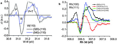 | ||
| Fig. 16 The PRS spectra for (a) the W(110), W(540) (0.16 ML) and (320)(0.28 ML) surface,131–134 and (b) the Rh(111) vicinal (553) (0.26 ML) and (151513) (0.07 ML) surfaces127 and the missing-row type reconstructed Rh(100) surfaces with same edge density (0.5 ML) but slightly different atomic CNs.128 Components above the bulk valley correspond to the polarization screening and the components below to the trapped states. The valley at lower energies represents the effect of T and P coupling. | ||
From the comparison, it is suggested that the under-coordinated W atoms could be an alternative donor in catalytic reactions, though the functionality of W is subject to further verification. Nevertheless, the PRS provides a powerful means for catalyst design and identification.
The findings presented can be extended to other under-coordinated atoms. For instance, the change of surface charge distribution caused by electrons trapped at defects of a SiO2 surface has been observed by using a mirror electron microscope (MEM) under monochromatized ultraviolet (UV) light irradiation.138 Scratches on the SiO2 surface deposited on a silicon wafer were formed by mechanically polishing to create spatially distributed defects on the SiO2 surface. Exposure of the SiO2 surface to UV light with energy above 4.25 eV that is the threshold energy for internal photoemission from silicon to SiO2, produced significant change in the contrast in the MEM images. This contrast change is mainly due to negative charging by the photoexcited electrons trapped at the defects along the scratches. The density of the scratch trapped electrons was estimated to be 1010 cm−2.
Most strikingly, the PRS has been able to correlate the STM/S to the XPS and clarify the physical origin of the vacancy-induced states in various bands. The physical picture is now clear. The broken bond induces local strain and quantum entrapment with an associated densification and entrapment of the core charge and energy. The densely and deeply trapped charge in turn polarize the otherwise conducting electrons, leading to the STM/S mapped protrusions and the Dirac resonant EF states. The polarization of the nonbonding electrons will in turn partially screen and split the crystal potential, giving rise to the P states in the core bands. This procedure holds generally true for under-coordinated systems with nonbonding electrons such as the otherwise conducting electrons in the half-filled s-orbit of Ag(5s1), Au(6s1), Rh(5s1), etc, as demonstrated. The situation may change if the nonbonding electrons are absent such as in Co(4s2). Anomalous states also exist such as W(5d46s2) because of the complicated valance charge configuration.
5.3 Diluted magnetism: defect locked dipoles
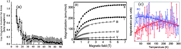 | ||
| Fig. 17 (a) Size dependence of the magnetic moments of Rhn(5s1) particles measured at low temperature shows the size-enhanced and quantized MS(Nj) with oscillating features.129,144(b) Molar magnetization at 1.8 K of Pt13 clusters on NaY substrate before (I) and after (II) hydrogen desorption,142 compared with that of Pt nanoparticles of 2.3 nm (420 atoms, III), 3.0 nm (940 atoms, IV) and 3.8 nm (1900 atoms, V)143 (c) Temperature dependence of Pd(5s04d10) nanoparticle magnetizations under zero-field cooling (ZFC) and field cooling (FC).139 | ||
In order to confirm the defect magnetism of GNR, we have recently calculated the effect of quantum entrapment and polarization and the magnetism of graphene vacancy and edges of the AGNR, ZGNR and rec-ZGNR, using the BOLS incorporated tight-binding mean-field Hubbard model. Results shown in Fig. 18 suggest that in addition to the global quantum entrapment of the under-coordinated vacancy and edges, the Dirac resonant peak presents only at the vacancy and the ZGNR edges. The midgap Dirac states are associated with non-zero magnetism, spin up and down. We also found from the calculations that the zigzag edges exhibit EF resonant states with non-zero spin and it is more significant to the reconstructed GNR edge.
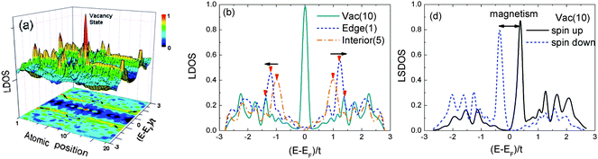 | ||
| Fig. 18 (a) The LDOS contour plot of the AGNR shows the EF resonant states localized at vacancy position 10, being consistent with that observed from graphite surface vacancies;7 (b) comparison of the LDOS at vacancy, edge, and the GNR interior. (d) The spin-resolved LDOS shows only atomic vacancy magnetism. | ||
As for d0 ferromagnets, reports exist for nitrides and hexaborides, for thiol-coated noble metal nanoparticles, purely organic systems, and even for silicon, with a spin-split impurity band near the EF, being coincidence with that generated by the lone pairs or the dipole states as we have discussed.
In contrast to the magnetism displayed by nanoclusters of noble metals and graphene nanoribbons, the diluted magnetism displayed by nanostructured oxides is mainly the result of dipoles at surfaces, instead of the locked dipoles due to polarization of unpaired electrons. However, in the presence of additional O atoms, these dipoles give away the polarized electrons to form bonds with the former, which leads to a reduction of the magnetic character, in the same way as hydrogen surface termination. A Curie temperature higher than 400 K corresponds to a lone pair interaction of ∼0.05 eV (600 K) and the UV reversion corresponds to the removal of surface contamination or dehybridization of sp orbits that diminish the surface dipoles. The presence of antibonding dipoles at the open surface may correspond to and increase the oxygen vacancies as referred to above.
However, I have three reservations on the under-coordination-induced dipole magnetism for practical applications. Firstly, the stability of the magnetrons with energy in the Fermi level and binding energy in meV level. Any perturbation by UV irradiation or thermal excitation may demolish them. Secondly, chemisorption by exposing the sample to the environment may decrease the magnetism. Finally, the intensity, as shown in Fig. 17 and Fig. 19, depends on the total number of defects. The weak magnetism may not be sufficient for the sensitivity requirement of practical devices.
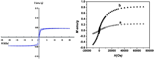 | ||
| Fig. 19 Magnetization curves of (a) the graphite nanostructures prepared by pyrolysis of PVC 1273 K and measured at 4 K by a SQUID magnetometer under a maximum applied field of 20 kOe,146 and (b) graphene samples fabricated at (a) 400 and (b) 600 °C measured at 2 K.145 High-temperature preparation generates more defects. | ||
5.4 Conductor–insulator transition: band gap opening and surface plasmonics
By combining STM and high-resolution EELS, Jiang et al.153 found that the band gap of two-dimensional Al islands grown on Si(111) substrates increases with decreasing island size. On the other hand, these originally highly conductive materials are no longer conducting; they become insulators instead when the solid size is reduced to 2–3 nanometres.154 It has been reported that the conduction band splits into two branches in ultrathin films such as Ag, Au, Pd, etc.58,59,155 The separation between the branches expands with the inverse of film thickness.The transition from conductor to insulator of noble metal clusters was ever attributed to the expansion of the Kubo gap: δk = 4EF/3N, where EF corresponds to the Fermi energy of the bulk and N to the total number of atoms in the cluster. If the δk is greater than the energy kT at room temperature (1/40 eV), electrons cannot transit from the lower sublevel to the next higher one, conductor–insulator transition takes place.154 The band gap opening was also attributed purely to the size effect arising from the lateral confinement of free electrons in a 2D potential well formed by the islands.153
However, as an intrinsic contribution, the polarization of the valence electrons near the upper valance edge by the densely-trapped bonding and core charges could not be ignored. The mechanism of band splitting by quantum entrapment and polarization may complement the formerly mentioned mechanisms. The conductor–insulator transition is evidence of the skin depth quantum entrapment and polarization of the conductive electrons. Therefore, both the conductor–insulator transition and the magnetism of metal clusters arises from the same origin.
The observed conduction band splitting may provide possible mechanism for the surface plasma generation of nanoclusters of noble metals such as Ag and Au with oscillation frequency that is dependent upon the dielectric constant, εL, charge density, n, and effective mass of electron, m*, in the surface skin. The plasmon frequency can be derived as 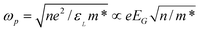 as the real part of the dielectric constant εL is inversely proportional to the square of the band gap roughly.64,156 Therefore, the observed edge and surface states due to band splitting may be responsible for the tunable plasmon frequency or the surface enhanced Raman shift intensity of selected metal surfaces and nanostructures. In addition to the classical model of surface plasma oscillation, the model of valence band splitting may provide a band structure perspective, as optical properties of a material are related to the band structure.
5.5 Coulomb repulsion at the nanoscaled elastic contacting interface
Superhydrophobicity, superfluidity, superlubricity, and supersolidity (4S) at the nanometre-sized liquid–solid or solid–solid contact interfaces are indeed fascinating, which have continued stimulating interest for decades.103 The 4S phenomena that share the common characteristics of chemically non-sticky, mechanically elastic and frictionless motion are of great importance not only to practical applications but also to the fundamental understanding of interactions between the nanometre-sized contacts. Unfortunately, the underlying mechanism remains unclear despite various modeling theories in terms of:(i) Young's theory in terms of surface tension and interface energies.157
(ii) Wenzel–Cassie–Baxters' law158,159 of surface roughness for superhydrophobicity.
(iii) Electrical double layer (EDL) scheme for the superfluidity.160
(iv) Prandtl–Tomlinson (PT) theory161,162 of the superposition of the slope of atomic potential and multiple-contact effects163 for atomic scale quantum friction.
(v) Anderson's theory164 of local vacancy density enhancement of crystal imperfections and the Bose–Einstein condensation theory for the superelasticity and superfluidity of the individual segment of the 4He crystal supersolidity.
However, some amazing observations are beyond the expectation of the above theories. Considerations from the perspective of surface roughness and surface energy seem insufficient because the chemistry and the charge identities alter at the surface skin up to two interatomic spacings.165 In particular, the hydrophobicity–hydrophilicity recycling effect caused by UV irradiation and the subsequent dark aging is beyond the scope of Cassie's law and the PT mechanism of air pockets dominantes. Furthermore, the superhydrophobicity of alkanes, oils, fats, wax, and the greasy and organic substances composed of C, N, O, or F as the key constituent element, is independent of the surface roughness. Although the atomic vacancies near crystal defects have been recognized as the key to the supersolidity of 4He solid, a correlation between the defects and the superelasticity and superfluidity is yet to be established.
From the perspectives of chemical bonding and the unusually electronic and energetic configurations in the surface of skin depth, we103 proposed that the Coulomb repulsion between the “electric dipoles locked in the elastic solid skins or the solid-like elastic liquid skins” forms the key to the 4S. According to the BOLS theory, localized densification of charge and energy takes place in the surface of skin depth.55,100 The energy densification enhances the local elasticity50 or stiffness (the product of the skin thickness and the elastic modulus) of the skin and the densely- and tightly-trapped charges will polarize existing surface nonbonding electrons. The localized polarization of the surface nonbonding s-electrons makes Au(6s1), Ru(5s1), Rh(5s1), and Ag(5s1) nanocrystals nonconductive and magnetic,3 because the otherwise conducting electrons turn to be the tightly-locked dipoles.
As illustrated in Fig. 20, the charge density, elasticity, and the quantum trap depth increases with the surface curvature or atomic CN reduction. The presence of lone electrons or lone pairs will generate the locally locked dipoles; Coulomb repulsion between them will be responsible for the observed 4S. Within skin depth of the surface, the charge density (ni) and energy density (elastic modulus, Bi follow the relations:1ni = nbC−3iBi = BbC−(m+3)i. By using nanoindentation, one can readily measure the surface hardness to gain information about the surface energy density. The hardness of the TiCrN surface skin was measured to be twice that of the bulk interior, evidencing the broken-bond-enhanced surface energy density.98 It has been found74,75 that the liquids of Bi, Sn, Ga, In, and K are also capped with a strained layer of atoms with a charge density higher than that of their bulk solids. For instance, the spacing between the first and second layers of Sn contracts by 10%.74 A recent experimental work revealed that the surface charge of confined water can induce a strong surface field that promotes the formation of a thicker water lubrication film on oxide. The liquid droplet is indeed capped with a solid-like and elastic skin166 with tightly-trapped charges due to the universal surface bond contraction and quantum entrapment of energy and charge.
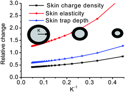 | ||
| Fig. 20 BOLS derived curvature dependence of the skin charge density, elasticity, and the quantum trap depth compared with a flat surface.103 The repulsion between the electric dipoles locked in the elastic solid skins or the solid-like elastic liquid skins provides the force driving the 4S and elaborates Wenzel–Cassie–Baxter's law of hydrophobicity and hydrophilicty enhancement by surface roughening. If there is no dipole formation, the roughened surface will be hydrophilic. | ||
A recent first-principles investigation167 suggested that charged surface dangling bonds in Si nanostructures provide traps for mobile carriers that become more stable as the size of the nanostructure is decreased, which implies that the charged dangling bonds on Si nanostructures can be fundamental obstacles in nanoscale doping, and this dopant deactivation becomes stronger as they become smaller. The asymmetric doping efficiency between p-type and n-type doped Si nanostructure is attributed to the preference for negatively charged acceptor-like dangling bonds over positively charged donor-like ones owing to a larger quantum entrapment and polarization effect in the conduction band.
UV radiation with excitation energy around 3.0 eV could break chemical bonds and ionize surface atoms, which can turn a hydrophobic surface hydrophilic, as it has widely been observed. Ar+ sputtering the surface is expected to have the same effect of temporarily removing dipole or monopole. If the polarized electrons are removed by UV irradiation, sputtering, or thermal excitation, the 4S characteristics would be lost. Aging of the specimen will recover the surface charges. The effect of UV radiation reversing effect is the same as that observed in the surface magnetism of noble metal clusters and the diluted magnetism of oxide nanostructures.3,142,150 Experimental investigations13 revealed that thermal annealing at temperatures of 600 K or above, oxygen orbital de-hybridization takes place and the lone pair induced Cu surface dipoles vanish. However, aging the samples in ambient conditions will recover the sp-hybridization and the dipoles as well. It is expected that surface bias, to a certain extent, may also cause the depletion of the locked charges though this expectation is subject to verification. Overloaded pressure in dry sliding will overcome the Coulomb repulsion, as the energy dissipation by phonon and electron excitation could occur under the applied pressure. On the other hand, if there is a sufficiently large difference in the electro-affinity between the contact media, a chemical bond may form under a certain conditions such as heating, pressure, or an electric field, and the interface will be adherent.
When two bodies of negative charges are placed together, interfacial Coulomb repulsion will be established, which lowers the contact pressure and hence the frictional force. This process is independent of the drying or vacuum conditions or the applied pressure. However, if the applied pressure is too large compared with the Coulomb repulsion, situation may change – kinetic energy dissipation takes place during sliding motion. If either side of the counterpart of friction is positively charged such as by H+ termination168 or hole (+) accumulation,169 an attractive force will be established and the friction will be enhanced.
The small fluidic drop can be viewed as a liquid core capped with a solid-like, densely charged, and elastic sheet of locked dipoles or dipoles at the surface. If the liquid–solid contacted counterparts are both negatively charged, charge sharing could not happen and the interface sticking could be thus prevented. The liquid droplet will react repulsively and elastically to the contacting body of which the surface is also negatively charged. If the droplet is sufficient small, the repulsion may levitate it – giving rise to superhydrophobicity. The findings of the correlation between the surface dipole and contact angle by Giovambattista et al.170 may provide evidence for this understanding. In the outermost two atomic layers of a smaller droplet, the energy density is even higher, the potential trap is even deeper and the effect of trapping and polarizing is even more apparent. The liquid drop and the channel wall surface are both negatively charged and they repel each other without sticking to the counterparts. The droplet will lose its viscosity and becomes elastically frictionless. Such a system runs in a way more like a “magnetic levitation train” or a “hovercraft”. Therefore, it is clear why surface roughening makes the hydrophilic surface more hydrophilic and the hydrophobic one more hydrophobic as indicated by Wenzel–Cassie–Baxters' law. The surface roughening lowers the surface atomic CNs enhancing the quantum entrapment and polarization effect.103
The Coulomb repulsion between the “dipoles locked in the stiffened skins” of the small grains could help in understanding the puzzle of 4He crystal supersolidity in real space. The densification of energy corresponds to an enhancement in elasticity, which stiffens the solid skin allowing the 4He segment to react elastically to a shear stress; the repulsion between the charged surfaces makes the motion frictionless. The extremely weak interatomic interaction between the He atoms makes the 4He atoms or grains nonsticky – more like hard spheres with close filled electronic shells. The lack of sticking interaction between grains will lower the friction coefficient. Lattice contraction of the supersolid 4He segments is expected to happen, though this contraction may be too tiny171 and needs to be verified experimentally.
VI Prospective applications
• Broken bond-induced valance charge entrapment and polarization splits the valence band and occupation of the upper branch dominates the catalytic ability of under-coordinated systems.• The nonbonding lone pairs of O, N, and F could be responsible for low-frequency of vibration in the NTE, and the Fermi states could dominate the high TCsuperconductivity.
• The length and energy of the H2O intermolecular nonbonding change oppositely to that of the intramolecular bond under external stimuli.
• The inter- and intra-molecular cooperative interaction is suggested to be responsible for the anomalies of ice and spin ice glasses.
• Lone pair transition at the body temperature could originate DNA folding, NO signalling, and the functional of biological molecules.
6.1 Catalytic enhancement and catalyst design
Pollution from automobiles is emitted in the first 5 min after startup because Pt- or Pd-based catalysts currently used in automobile exhaust cleanup are inactive below a temperature of 200 °C. The low-temperature gold catalysts are very inactive unless the gold is in the form of particles smaller than 8 nm in diameter. However, self-ignition of Pt nanoparticles happens at room temperature by exposing the particles to methanol/air or ethanol/air gas mixtures. Designing efficient catalysts to work at low temperature for both oxidation and reduction is greatly desired for environment protection.Atomic under-coordination or hetero-coordination forms an optimal route, though mechanism still remains unknown. The primary role of under-coordinated atoms in determining the surface chemical reactivity has been well-established as a result of surface science. It has been found that2 with the every third row of Au atoms added to a fully Au covered TiO2 surface could improve the efficiency of CO oxidation at room temperature by a factor of 50 compared with the otherwise fully Au covered surface. In the case of N2 dissociation on Ru(0001) surface, the activation energy is 1.5 eV lower at step edges than that on the flat surface, yielding at 500 K a desorption rate that is at least nine orders of magnitude higher on the terraces, as the dissociation is largely influenced by the presence of steps.172 Similar results have been found for NO decomposition on Ru(0001),173,174 H2 dissociation on Si(001),175 and low temperature nitridation of nano-patterned Fe surfaces.176 An adatom concentration of a few percent is sufficient to dominate the overall reaction rate in a catalytic process because of the higher reaction rate or lower activation energies of the under-coordinated atoms. For instance, the first methane dehydrogenation process is highly favoured at the Rh-adatom site on the Rh(111) surface with respect to step or terrace sites;177,178 adatoms deposited on oxides can activate C–H bond scission,179 acetylene cyclomerization,180 and CO oxidation.181 Preferential NO uptake occurs at Rh(311) and (533) edges.182
The presence of defects opens new pathways which significantly decrease the thermal stability of the reconstructed Rh(110) surfaces.128 Although the activity of electrochemical oxidation of carbon monoxide and methanol electro-oxidation can be increased by increasing surface steps on Pt nanoparticles, the oxygen reduction reaction activity of the 2 nm sized Pt nanoparticle has been found insensitive to the step area, as shown in Fig. 21,183 in contrast to the methanol oxidation reaction activity.
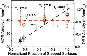 | ||
| Fig. 21 Step density dependence of the oxygen reduction reaction (ORR, right axis) and methanol oxidation reaction (MOR, left axis) of 2 nm Pt particles.183 | ||
Another relevant contribution determining the chemical reactivity is the surface strain. Gsell et al.184,185 found preferential oxygen and carbon monoxide adsorption on the stretched regions obtained through subsurface argon implantation on Ru(0001). Wintterlin et al.186 measured an enhanced NO dissociation probability at the local expanded areas of the Ru(0001) dislocations. In the case of a supported nanoparticle catalyst, it has been observed that adsorption on small clusters can induce a considerable stress in the surface region.187 In any case, the existence of strain, originating from surface defects or by the interaction with the support, seems to be a general feature of surface catalysts. Using an indirect nanoplasmonic sensing method, Langhammer et al.188 observed strong size effect in studying the hydriding and dehydriding kinetics of Pd nanoparticles in the size range 1.8–5.4 nm. The size trend agrees well with the simulated diffusion-controlled hydriding kinetics. They attributed this trend to surface tension on hydrogen desorption from the surface layer.
A possible mechanism for the under-coordinated Au catalyst enhancement has been proposed as follows.2 The catalytic activity of gold was attributed entirely to the presence of neutral gold adatoms. These adatoms differ from atoms on bulk gold in three ways that might enhance their catalytic activity:2 (i) they have fewer neighboring atoms and possibly a special bonding geometry to other gold atoms that creates a more reactive orbital. (ii) They exhibit quantum size effects that may alter the electronic band structure of gold nanoparticles. (iii) They may undergo electronic modification by interactions with the underlying oxide that cause partial electron donation to the gold cluster. It is noted that the under-coordination enhanced CO oxidation catalytic reactivity of Au/TiO2 monatomic chains and Au/oxide2 nanosolid agrees with the BOLS prediction of the size dependence of diffusivity with activation energy being proportional to atomic cohesive energy or the critical temperature of melting. The similarity in the trends of atomic diffusivity and chemical reactivity indicates that these two identities are correlated in terms of activation energy, though the former is related to atomic dislocation while the latter to charge capturing.
Obviously, the ability of a catalyst to accept or donate charge plays a key role in the process of catalytic reactions.3 The direction of electronic transfer between the gold atoms and the underlying oxide, and between the gold and the CO gas need to be clear, which may form the key to the catalytic activity of these under-coordinated catalysts. An atomic-level understanding of the local energetic behavior of electrons of low-dimensional systems and their mechanical properties become especially important in systems with a large number of highly under-coordinated atoms.
The objective of catalytic enhancement and catalyst design is to modulate the electronic structure in the upper edge of the valence band. One can create vacancies on the valance band edge or can raise the occupied valence states towards the EF. Therefore, the catalyst can serve as acceptor or donor, respectively. According to the BOLS correlation, the under-coordination induced quantum entrapment and nonbonding charge polarization provide a possible means. Strain or stress is a consequence of the surface bond contraction and quantum trapping, and therefore, valence DOS and strain are correlated. Therefore, the involvement of the broken bonds and the nonbonding paired and unpaired electrons plays a significance role in complex processes such as the CO ↔ Au ↔ oxide reaction. It is also expected that a suitable size range may exist for Pt and Pd catalysts to be reactive at room temperature without ignition. The electroaffinity is tunable by the cluster size through valence charge polarization or quantum trapping.189 The stress is related to the quantum trapping through interatomic binding energy variation. Hence, the ability of a catalyst to accept or donate charge is controllable by varying the atomic coordination.
The purified energy states of Pt and Rh adatoms,6 graphite surfaces and vacancies,7 shown in Fig. 15, and the purified valence DOS of Ag/Pd and Cu/Pd alloys, see Fig. 22,46 provide guidelines for catalyst design. The under-coordinated Pt acceptor6 tends to catch electrons from the gaseous specimen rather than to donate, which may explain the active oxidation and the inactive reduction and the charge flow direction between the Pt nanocatalyst and the gaseous specimen in the processes of reduction and oxidation (see Fig. 21). Likewise, CuPd performs the same in the process of reaction. In contrast, Rh adatoms and Ag/Pd surface alloy donate their valence charge to the gaseous specimen in reaction, in the opposite way to Pt and the Cu/Pd alloy.
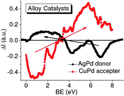 | ||
| Fig. 22 PRS purified valence DOS showing the charge flow direction upon alloy formation suggests that the Ag/Pd surface alloy serves as a donor and Cu/Pd as an acceptor in the process of catalytic reaction.46 | ||
We suggest that a high degree of under-coordination or proper hetero-coordination by alloy or compound formation could be effective approaches for the efficient catalyst design because the broken bond and interface bond induced quantum trapping and polarization that determines the direction and extent of valence charge flow between the gaseous specimen and the catalyst.
6.2 Hydrogen bond dynamics: ice and NTE
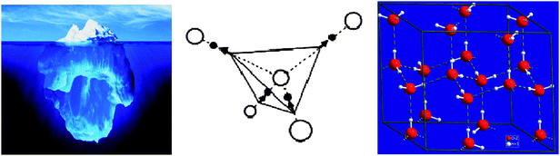 | ||
| Fig. 23 (a) The low-density of an iceberg, (b) the schemes of Pauling's “two-in two-out” ice rule for water and spin ice glass molecules and, (c) the hexagonal ice structure. The tetrahedrally coordinated oxygen is surrounded with four H+ neighbors and each H+ connected with two O2− neighbors. For each H+ proton, there are two equivalent positions but for an O2−, two H+ protons are in the near and the rest two are in the far positions, leading to the frustration. | ||
Pauling20 proposed an “two-in two-out” ice rule and showed that ice possesses a finite entropy (estimated as 0.81 cal K−1 mol−1 or 3.4 J K−1 mol−1) at zero temperature due to the configurational disorder intrinsic to the protons in ice. Fig. 23(b) illustrates Pauling's ice rule for water and spin ice glass molecules and (c) the hexagonal ice structure. In the hexagonal or cubic ice phase the oxygen ions form a tetrahedral structure with an O–O distance of 0.276 nm, while the intramolcular O–H bond length was measured only 0.096 nm using XRD and 0.10 nm using nuclear magnetron resonance. Every oxygen (white) ion is surrounded by four hydrogen ions and each H+ is connected by two O2−. Maintaining the internal H2O molecule structure, the minimum energy position of an H+ proton is not halfway between two adjacent O2−. There are two equivalent positions that an H+ may occupy on the O–O line, a far and a near position. Thus a rule leads to the frustration of positions of the proton for a ground state configuration: two of the neighboring protons of oxygen must reside in the far position and the rest two in the near position, so-called ‘ice rules’. Pauling48 proposed that the open tetrahedral structure of ice affords many equivalent states satisfying the ice rules. Unfortunately, the correlation between the hydrogen bond on the density anomalies of ice has yet to be established.
Various mechanisms have been developed to explain the NTE in compounds. The models include transverse thermal vibrations of bridging oxygen in the M–O–M linkages198 in ZrW2O8, HfW2O8, the SC2W3O12, AlPO4–17, and faujasite SiO2.199 The low frequency phonon modes (centered around 30 meV),99 see Fig. 24, can propagate without distortions of the WO4 tetrahedra and ZrO6 octahedra, which is called ‘rigid unit mode’. The rigid-unit mode also accounts for the weak effect of the 430 K structural phase transition on the NTE.200 However, the physical origin for the low frequency vibration remains unclear. Fig. 24 also compares the regular thermal expansion coefficients of AlN, GaN, and Si3N4, which follows the trend of Debye approximation of specific heat.201
 | ||
| Fig. 24 (a) ZrW2O8 phonon density of states measured at T = 300 K.99 (b) Temperature dependence of the lattice parameter a (open circles) and Grüneisen parameter γ = 3αB/Cv, (crosses) of ZrW2O8. Parameters α, B, and Cv correspond to thermal expansion coefficient, bulk modulus and the specific heat at constant volume, respectively. (c) The positive thermal expansion coefficient of AlN, GaN, and Si3N4 for comparison.201 | ||
From the perspective of hydrogen bonds and hydrogen-like bonds in oxides and nitrides,12,13 we proposed, as illustrated in Fig. 25, a linear O2−:H+/p–O2− configuration. The H+/p represents the ionized dipole that provides an electron for bonding, and can be replaced by any element with electronegativity lower than that of oxygen. The O2− can also be replaced by F− and N3− ions. 2H+/p–O2− forms a molecule. The intramolecular H+/p–O2− bond is much shorter and stronger than that of the O2−:H+/p intermolecular nonbond. The interaction energy for the former is several eV but the latter only 30–80 meV, in the frequency of tera-Hz, or lower than 1000 cm−1 wavenumbers.13
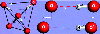 | ||
| Fig. 25 (a) Schematic illustration of the new “bond contraction nonbond expansion” ice rule and the 2H2O tetrahedron with the “two-in two-out” H2O model included. (b) The stronger intramolecular H+/p–O2− bond contracts following the regular rule of thermal expansion and BOLS correlation while the weaker H+/p:O2− nonbond expands when the bonding pair of electrons come closer to the central H+/p due to the polarization of the lone pair “:” by the close-moving densely trapped bonding electron pair. The net distance of the O2−:H+/p–O2− expands simultaneously and identically when temperature drops, resulting in the density anomalies of ice. Applying pressure reverse the processes of low-T and low-z. | ||
Based on the above considerations, we carried out an MD calculation, from which it turned out that when the temperature is lowered from 270 to 250 K, the H+/p–O2− bond contracts from 0.0796 to 0.0793 nm and meanwhile the H+/p:O2− nonbond expands from 0.1675 to 0.1800 nm with a net expansion of ∼4.9%, of which the projection (sin(128.5°/2) = 0.9) along a given direction agrees fairly well with the known 3.54% linear or the 11% net volume expansion of ice. The accuracy can be realized by optimizing the inter- and intra-molecular potentials. The expected bond contraction and nonbond expansion of H2O is consistent with what happened to the Cu3O2 bonding kinetics at Cu(001) surface.87 VLEED optimization of the Cu3O2 bonding dynamics has revealed that when the Cu+–O2− length contracts from 0.1850 to 0.1776 nm, the Cup:O2− distance expands simultaneously from 0.1817 to 0.1950 nm.
• The length and energy of the intramolecular H+/p–O2− bond and the intermolecular H+/p:O2− nonbond change oppositely under the externally applied stimuli of temperature (T), pressure (P), and coordination number (z), originating the unusual properties of ice and the NTE.
• Unlike the situation discussed in section III, the effect of P increasing is opposite to that of T and z dropping on the H bond length and energy; both T decreasing and z dropping have the same effect.
The H+/p–O2− bond is suggested to follow the regular rule of thermal expansion201 and the BOLS correlation while the O2−:H+/p nonbond does not. The latter expands when the former contracts; if the bonding electron pairs come closer to the central H+/p the lone pair is pushed away from the center because of the polarization. Therefore, the density of ice will drop with temperature. Likewise, the volume expands when the molecular coordination z is reduced, which is the case of a monolayer or a thin layer of water. If pressure is applied, the O2−:H+/p nonbond responds first because of the high compressibility that is proportional to the inverse of energy density. Using MD simulations, Wang et al.203 found that a monolayer of water at room temperature exhibits “quasi-solid” nature that prevents the monolayer from being wetted by a water droplet. This finding may explain the size effect that could raise the melting point of the monolayer water.
Table 3 summarizes expectations with evidence of computational and experimental observations on the unusual performance of ice and materials with H-bond involvement. It can be seen that there is plenty of work that needs to be done, and more computational and experimental investigations are being carried out in my group.
| Expectation observation | Low z (BOLS) | Low T | High P | Anomalies |
|---|---|---|---|---|
| Intramolecular H+/p–O2− bond | Contraction87,204 energy gain205–208 | Contraction energy gain | Expansion209 energy loss | |
| Intermolecular H+/p : O2− nonbond | Opposite to the H+/p–O2−87,204,205,209 | Hydrophobicity;170,203 fragility; slippery; Tm; Tevp. High heat capacity; high compressibility | ||
| Density | Decrease | Increase210 | ||
| Acoustic mode | Red shift | Blue shift211–214 | ||
| Optical mode | Opposite to Acoustic vibration | |||
Fig. 26 shows the consistency between the present expectation and computation results of the correlation of the O2–H+/p and O2− : H+/p distances in hydrogen bonds,208 Experimental measurement under high pressure209 also revealed the same trends. As expected, the (b) in situ Raman spectra of ice VIII at 80 K revealed blue shift in the (b) low acoustic frequency (200–400 cm−1) and (c) redshift in optical mode (2800–3500 cm−1) as the pressure is increased.213 The former corresponds to the intermolecular H+/p:O2− weak interaction and the latter to the intramolecular H+/p–O2− stronger interaction. As shown in section 3.1, the Raman shift depends on the atomic distance, bond order, and energy and the reduced mass of the bonding atoms or molecules in the form of: ω ∝ z(Ei/μ)0.5/d.
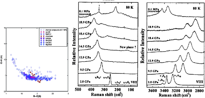 | ||
| Fig. 26 (a) Correlation of the O–H and O:H distances in O–H:O hydrogen bonds,208 (b) in situ Raman spectra of ice VIII at 80 K in the regions of (b) rotational and translational frequency (200–400 cm−1) and (c) O–H stretching vibrations (2800–3500 cm−1) as a function of pressure.213 Increasing pressure induces blue shift to the low-frequency acoustic mode and redshift to the high-frequency optical mode. | ||
We may explain the slippery or low-friction of ice surface215 as results of the lone pair weak yet elastic interaction and the high density of surface charge instead of liquid lubrication. Furthermore, because of the cohesive energy gain of the two intramolecular O2−–H+/p bonds, a monolayer of water acts solid-like with high elasticity and charge density because of the increase of molecular cohesive energy that raises the melting point. This expectation has been proved using thin film interferometry by Liu et al.216 who have found a higher surface charge density. The strong surface field induced by the surface charge establishes a more ordered hydrogen bonding network that promotes the formation of a thicker water lubrication film between hydrophilic solid surfaces. This mechanism is the same as that of superhydrophobicity, discussed in the section 5.5.
It is also suggested that the weak “:” interaction is responsible for the “rigid-unit mode”, the 430 K structural phase transition, and the NTE of ZrW2O8.195,200 The low-frequency of vibration of 30–40 meV99 of ZrW2O8 is in the same order of N and O induced Raman shift of ∼500 cm−1 (Fig. 8d) and the frequency detected from many oxide surfaces.13 The low frequency corresponds to the lone pair vibration in tera-Hz range. The findings may also explain the anomalous increase of the distance between copper oxide planes on cooling,193 which results in negative thermal volume expansion, for layered ruthenium copper oxides that have been doped at the boundary of antiferromagnetism and superconductivity.
6.3 B-, C-, N-, O-, F-induced high-Tc superconductivity
The original Bardeen–Cooper–Schrieffer (BCS) theory of superconductivity adequately described the origin and behavior of conventional superconducting metals and alloys, whose critical temperatures of transitioning to superconductivity are extremely low, never higher than 30 K. According to the BCS theory, superconductivity is governed by a large Bose–Einstein condensation, resulting from the coupling of electron pairs near the Fermi surface, which are known as Cooper pairs, at low temperatures. However, in 1986 and subsequent years, copper oxides were discovered to become superconducting at temperatures up to 136 K and even 160 K when this new type of material were subjected to pressure. The emergence of the new “high-TC superconductor” also marked the start of a revolution in its applications as well as scientific hypotheses regarding it, because the BCS theory was evidently inadequate.The fact that some compounds of B, C, N, O, Se, P, and F and other elements exhibit high-TC superconductivity, albeit at different critical temperatures, implies an underlying similarity in these inducing elements. Fortunately, it has been certain, as discussed, that in N, O and F, the sp3-orbit hybridization generates the nonbonding and antibonding states near the Fermi surface (see Fig. 6). In turn, these localized lone pair electrons and highly energetic antibonding electrons may have a high chance of forming Cooper pairs which dominate the character of the high-TC superconductor. When an external electric field is applied, these localized pairs of electrons are easily excited and hence become highly conducting when given suitable channels of penetration. Compared with the findings of graphene nanoribbon edge states,9,10 the effective mass of these electrons is expected to be very small and their group velocity very high.
An important characteristics to note is that these high-TC superconductors all assume a two-dimensional layered structure, such as Cu–O chains or planes, on which superconductivity mainly occurs. Most strikingly, the unique “Cup:O2−:Cup:” chains on the copper surfaces upon O adsorption with generation of diploes and lone pairs have been identified.13 Bound energy states near the Fermi surface in oxide superconductors217 has also been confirmed using UV photoemission spectroscopy, further corroborating the importance of antibonding and nonbonding impurity states in effecting superconductivity.
As a possible mechanism governing the high-TC superconductivity, the strong correlation of electrons with spins has attracted much attention in recent years. However, the presence of the nonbonding and the antibonding states near Fermi surface should play at least a role of competence. If the 1s-electrons of B and C are excited to occupy the hybridized 2sp3 orbits, B and C would likely form valence band structures similar to those of N and O and hence resulting in the superconductivity. The exposition of the mechanism of high-TC superconductivity from the perspective of antibond and nonbond formation and the corresponding electronics and energetics would be a revolutionary approach culminating in a breakthrough.
6.4 CF4 anti-coagulation in artificial blood
A key unresolved challenge in creating artificial blood is anti-coagulation. In 1998, Professor Huang Weiheng from the Institute of Organic Chemistry, Chinese Academy of Science, discovered that CF4 is an excellent artificial blood anti-coagulant, whose microscopic mechanism is, however, not yet fully understood. Our current discussion on the sp orbital hybridization of C and F and the presence of nonbonding states could be applied in this instance. As illustrated in Fig. 27, the sp orbits of C and F undergo hybridization to form tetrahedra. A central C4+ ion is surrounded by 12 pairs of nonbonding electrons, resulting from the four surrounding F− ions each carrying 3 pairs of nonbonding electrons. These lone pairs of electrons form a functional group that attracts and weakly polarizes nearby atoms, making them mobile in fluids because of this weak interaction, which translates to an anti-coagulating function. NF5 and SF6 also possess 15 and 18 lone pairs of electrons with structure being similar to CF4, respectively, and hence are predicted to display the same character as that of the CF4.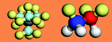 | ||
| Fig. 27 Hypothetic (a) CF4 (C4+ + 4F− + 4 × (3:)) and (b) NO (N3− + O2− + 3(−) +3(:)) molecules. (−) represents the dangling bond and (:) the nonbonding lone pair. | ||
6.5 NO and enzyme telomeres
All organic and living cells are composed primarily of H, C, N, and O. Similarly, most pharmaceutical products are also composed of these elements, apart from tiny amounts of dopant and their molecular configurations. For example, nitric oxide, NO, is a short-lived, endogenously produced gas that acts as a signaling molecule in the body. Signal transmission by the gas, produced by one cell, which penetrates membranes and regulates the function of other cells is an entirely new principle for signaling in the human organism. NO can not only be used to combat many arterial-related diseases, but also plays an important role in molecule signaling outside the cardiovascular system and has become a useful tool in the practice of medicine. However, the bonding mechanism of NO is yet to be made clear.If the N and O atoms are linked by a single bond to form an NO molecule with hybridized sp3 orbits (Fig. 27b) of both, one side of the molecule has three lone pairs while the other has three dangling bonds, or twisted by 180°. Such a structure enables the NO molecule to be located at a certain place by forming bonds via the dangling ones and meanwhile polarize its surroundings via the lone pairs, producing regulation channels required in medication. Under certain chemical conditions, the molecular orbits of NO can hybridize or de-hybridize to alter their functionalities. In the body, on the other hand, the lone pair electrons and antibonding dipoles produced by O, N and C are mainly responsible for the synthesis, folding and unfolding mechanisms of cells, protein, DNA and RNA as well.
The understanding of lone pairs, dipoles, and the broken bonds may be extended to the function of enzyme telomere capped chromosome ends, see SEM image in Fig. 28, exhibits the abnormal end states with the similar characteristics as discussed above..218 The protection of chromosomes by telomeres is associated with aging, cancer, and heart diseases. This discovery was awarded the 2009 Nobel Prize in physiology. Further investigation would be interesting and awarding.
 | ||
| Fig. 28 Scanning electron microscopy of enzyme telomere caps on chromosome ends. | ||
VII Conclusions
I have thus far discussed, with evidence and suggestions of potential applications, the significance of the nonbonding lone electron pairs and the lone pair-induced dipoles associated with the process of tetrahedron bond formation of C, N, O, and F and the under-coordination-induced quantum entrapment of the core and bonding electrons and lone electron polarization. The impact of these often overlooked interactions and the associated energy states in the midgap region is enormous, in particular at the nanoscale. These weak interactions and charges can never be neglected when we attend to substances at the nanoscale. The opposite trends of length and energy change of the two parts of the H-like bond are the origins of the density anomalies of ice and the NTE coefficient of compounds. The coupling of quantum entrapment and polarization makes a great deal of difference such as the enhanced catalytic and the observed 4S. These weak interactions and nonbonding electrons also form basic function groups in the biologic, organic and inorganic species. Table 4 summarizes the classification, origins, functions and possible applications of the bonds and nonbonds.| Bond and DOS | Origin | Functions and applications |
|---|---|---|
| Regular bonds (≪EF) | Strong interaction, charge sharing | Hamiltonian; atomic cohesive energy; band structure; dispersion; allowed DOS in valence band and below; mainly bulk properties. |
| Electronic hole (<EF) | Charge transition in reaction, positive ions. | Compound band gap formation; semiconductor band gap expansion; photon emission and absorption, photonic sensor |
| Antibonding dipole (>EF) | Induced by lone pair polarization or under-coordination induced local core charge densification | Impurity states generation; work function reduction; surface dipole layer formation; surface energy density gain; electron cold field emission; superhydrophobicity; defect magnetism, etc |
| Nonbonding lone pair (<EF) | N, O and F sp-orbital hybridization | Polarizing, functional groups in organic and biological molecules, impurity states generation; hardness and elastic modulation; quantum friction; infrared activity; magnetic modulation; drug design; density anomalies of ice, NTE, 4S; etc |
| H-like and C–H-like bonds | Bond formation between dipole and electronegative elemental atoms | Dipole state annihilation; work function recovery, impurity states annihilation; surface stabilization; surface passivation; antioxidation |
| Nonbonding lone electron (∼EF) | Defect, sp2 hybridization in C, half-filled s-orbit of noble metals | Midgap defect states; Dirac resonance; defect magnetism; end and edge states; 4S; graphite electrical conductivity; catalytic enhancement, etc. |
| Broken bonds | under-coordination | Modulation of bulk properties; structure relaxation; Hamiltonian, cohesive energy, electro-affinity modulation; local densification of charge, energy and mass; lone electron polarization; size dependency of all bulk detectable properties; band gap opening; etc. |
Utilizing the concepts of these unconventional types of weak interactions and their energetics, we can look forward to designing and synthesizing new functional materials. The approach of studying the formation, dissociation, relaxation, and vibration of bonds and nonbonds, and associated energetics and dynamics of electron transportation, polarization, localization, and densification effects on a microscopic level is essential to facilitating a deeper understanding of the macroscopic behavior of functional materials. In particular, the invention of photoelectron residual spectroscopy (PRS) has enabled us to purify information of bond and nonbond formation, charge and energy entrapment and nonbonding electron polarization in the atomic-scaled zones underneath that a STM/S can scope. It is more revealing than using XPS, UPS, AES, STM/S alone. With the developed knowledge and the specific PRS technique, we will be able to actively control the process of bond and nonbond formation towards knowledge creation and invention. Finding and grasping with factors controlling the nonbonding states and making them of use in functional materials design will form, in the near future, a subject area of “nonbonding electronics and energetics”, which would be even more challenging, fascinating, promising, and rewarding than dealing with core or valence electrons alone.‡
Acknowledgements
Financial support by Ministry of Education (RG15/09), Singapore, National Science Foundation of China (No. 10772157), Hunan Province, Jilin University, and the Key Laboratory of Ceramics and Refinery Processing at Tsinghua University, China and permission for reprinting diagrams from Elsevier, IOP, APS, ACS, NPG, AAAS, and AIP are all gratefully acknowledged.References
- C. Q. Sun, Size dependence of nanostructures: Impact of bond order deficiency, Prog. Solid State Chem., 2007, 35(1), 1–159 CrossRef CAS.
- M. S. Chen and D. W. Goodman, The structure of catalytically active gold on titania, Science, 2004, 306(5694), 252–5 CrossRef CAS.
- E. Roduner, Size matters: why nanomaterials are different, Chem. Soc. Rev., 2006, 35(7), 583–92 RSC.
- D. Q. Yang and E. Sacher, Strongly enhanced interaction between evaporated Pt nanoparticles and functionalized multiwalled carbon nanotubes via plasma surface modifications: Effects of physical and chemical defects, J. Phys. Chem. C, 2008, 112(11), 4075–82 CrossRef CAS.
- W. Liu, D. Liu, W. T. Zheng and Q. Jiang, Size and Structural Dependence of Cohesive Energy in Cu, J. Phys. Chem. C, 2008, 112(48), 18840–5 CAS.
- C. Q. Sun, Y. Wang, Y. G. Nie, Y. Sun, J. S. Pan, L. K. Pan and Z. Sun, Adatoms-Induced Local Bond Contraction, Quantum Trap Depression, and Charge Polarization at Pt and Rh Surfaces, J. Phys. Chem. C, 2009, 113(52), 21889–94 CrossRef CAS.
- M. M. Ugeda, I. Brihuega, F. Guinea and J. M. Gómez-Rodríguez, Missing Atom as a Source of Carbon Magnetism, Phys. Rev. Lett., 2010, 104, 096804 CrossRef CAS.
- Y. Niimi, T. Matsui, H. Kambara, K. Tagami, M. Tsukada and H. Fukuyama, Scanning tunneling microscopy and spectroscopy of the electronic local density of states of graphite surfaces near monoatomic step edges, Phys. Rev. B: Condens. Matter Mater. Phys., 2006, 73(8), 085421–8 CrossRef.
- T. Enoki, Y. Kobayashi and K. I. Fukui, Electronic structures of graphene edges and nanographene, Int. Rev. Phys. Chem., 2007, 26(4), 609–45 CrossRef CAS.
- C. O. Girit, J. C. Meyer, R. Erni, M. D. Rossell, C. Kisielowski, L. Yang, C. H. Park, M. F. Crommie, M. L. Cohen, S. G. Louie and A. Zettl, Graphene at the Edge: Stability and Dynamics, Science, 2009, 323(5922), 1705–8 CrossRef CAS.
- X. Zhang, J. L. Kuo, M. X. Gu, F.X.F., P. Bai, Q. G. Song and C. Q. Sun, Local structure relaxation, quantum trap depression, and valence charge polarization induced by the shorter-and-stronger bonds between under-coordinated atoms in gold nanostructures, Nanoscale, 2010, 2, 412–7 RSC.
- W. T. Zheng and C. Q. Sun, Electronic process of nitriding: Mechanism and applications, Prog. Solid State Chem., 2006, 34(1), 1–20 CrossRef CAS.
- C. Q. Sun, Oxidation electronics: bond-band-barrier correlation and its applications, Prog. Mater. Sci., 2003, 48(6), 521–685 CrossRef CAS.
- Y. B. Zhang, Y. W. Tan, H. L. Stormer and P. Kim, Experimental observation of the quantum Hall effect and Berry's phase in graphene, Nature, 2005, 438(7065), 201–4 CrossRef CAS.
- X. Du, I. Skachko, F. Duerr, A. Luican and E. Y. Andrei, Fractional quantum Hall effect and insulating phase of Dirac electrons in graphene, Nature, 2009, 462(7270), 192–5 CrossRef CAS.
- K. I. Bolotin, F. Ghahari, M. D. Shulman, H. L. Stormer and P. Kim, Observation of the fractional quantum Hall effect in graphene, Nature, 2009, 462(7270), 196–9 CrossRef CAS.
- K. S. Novoselov, Z. Jiang, Y. Zhang, S. V. Morozov, H. L. Stormer, U. Zeitler, J. C. Maan, G. S. Boebinger, P. Kim and A. K. Geim, Room-temperature quantum hall effect in graphene, Science, 2007, 315(5817), 1379 CrossRef CAS.
- K. I. Bolotin, K. J. Sikes, Z. Jiang, M. Klima, G. Fudenberg, J. Hone, P. Kim and H. L. Stormer, Ultrahigh electron mobility in suspended graphene, Solid State Commun., 2008, 146(9–10), 351–5 CrossRef CAS.
- A. A. Balandin, S. Ghosh, W. Bao, I. Calizo, D. Teweldebrhan, F. Miao and C. N. Lau, Superior Thermal Conductivity of Single-Layer Graphene, Nano Lett., 2008, 8(3), 902–7 CrossRef CAS.
- L. Pauling, The structure and entropy of ice and of other crystals with some randomness of atomic arrangement, J. Am. Chem. Soc., 1935, 57, 2680–4 CrossRef CAS.
- L. E. Brus, On the development of bulk optical-properties in small semiconductor crystallites, J. Lumin., 1984, 31–2(DEC), 381–4 CrossRef.
- A. I. Ekimov and A. A. Onushchenko, Quantum size effect in 3-dimensional microscopic semiconductor crystals, Jetp Lett, 1981, 34(6), 345–9.
- F. Koch, V. Petrovakoch, T. Muschik, A. Nikolov, and V. Gavrilenko, Some perspectives on the luminescence mechanism via surface-confined states of porous Si, in Microcrystalline Semiconductors: Materials Science & Devices, P. M. Fauchet, C. C. Tsai, L. T. Canham, I. Shimizu, and Y. Aoyagi, Editors. 1993, Materials Research Soc: Pittsburgh. p. 197–202 Search PubMed.
- G. G. Qin and Y. J. Li, Photoluminescence mechanism model for oxidized porous silicon and nanoscale-silicon-particle-embedded silicon oxide, Phys. Rev. B: Condens. Matter Mater. Phys., 2003, 68(8), 085309 CrossRef.
- Y. D. Glinka, S. H. Lin and Y. T. Chen, Two-photon-excited luminescence and defect formation in SiO2 nanoparticles induced by 6.4-eV ArF laser light, Phys. Rev. B: Condens. Matter Mater. Phys., 2000, 62(7), 4733–43 CrossRef CAS.
- C. Q. Chen, Y. Shi, Y. S. Zhang, J. Zhu and Y. J. Yan, Size dependence of Young's modulus in ZnO nanowires, Phys. Rev. Lett., 2006, 96(7), 075505 CrossRef CAS.
- Z. M. Ao, S. Li and Q. Jiang, The determination of Young's modulus in noble metal nanowires, Appl. Phys. Lett., 2008, 93(8), 081905 CrossRef.
- G. X. Cao and X. Chen, Size dependence and orientation dependence of elastic properties of ZnO nanofilms, Int. J. Solids Struct., 2008, 45(6), 1730–53 CrossRef.
- J. H. Song, X. D. Wang, E. Riedo and Z. L. Wang, Elastic property of vertically aligned nanowires, Nano Lett., 2005, 5(10), 1954–8 CrossRef CAS.
- B. M. Wen, J. E. Sader and J. J. Boland, Mechanical Properties of ZnO Nanowires, Phys. Rev. Lett., 2008, 101(17), 175502 CrossRef.
- G. F. Wang and X. D. Li, Size dependency of the elastic modulus of ZnO nanowires: Surface stress effect, Appl. Phys. Lett., 2007, 91(23), 231912 CrossRef.
- L. X. Zhang and H. C. Huang, Young's moduli of ZnO nanoplates: Ab initio determinations, Appl. Phys. Lett., 2006, 89(18), 183111 CrossRef.
- C. Q. Sun, Y. Wang, B. K. Tay, S. Li, H. Huang and Y. B. Zhang, Correlation between the melting point of a nanosolid and the cohesive energy of a surface atom, J. Phys. Chem. B, 2002, 106(41), 10701–5 CrossRef CAS.
- P. Buffat and J. P. Borel, Size effect on melting temperature of gold particles, Phys. Rev. A: At., Mol., Opt. Phys., 1976, 13(6), 2287–98 CrossRef CAS.
- P. R. Couchman and W. A. Jesser, Thermodynamic theory of size dependence of melting temperature in metals, Nature, 1977, 269(5628), 481–3 CAS.
- Q. Jiang, L. H. Liang and J. C. Li, Thermodynamic superheating and relevant interface stability of low-dimensional metallic crystals, J. Phys.: Condens. Matter, 2001, 13(4), 565–71 CrossRef CAS.
- K. K. Nanda, S. N. Sahu and S. N. Behera, Liquid-drop model for the size-dependent melting of low-dimensional systems, Phys. Rev. A: At., Mol., Opt. Phys., 2002, 66(1), 013208 CrossRef.
- M. Wautelet, Estimation of the variation of the melting temperature with the size of small particles, on the basis of a surface-phonon instability model, J. Phys. D: Appl. Phys., 1991, 24(3), 343–6 CrossRef CAS.
- W. H. Luo, W. Y. Hu and S. F. Xiao, Melting temperature of Pb nanostructural materials from free energy calculation, J. Chem. Phys., 2008, 128(7), 074710 CrossRef.
- G. Guisbiers and L. Buchaillot, Universal size/shape-dependent law for characteristic temperatures, Phys. Lett. A, 2009, 374(2), 305–8 CrossRef CAS.
- J. N. Crain, M. D. Stiles, J. A. Stroscio and D. T. Pierce, Electronic effects in the length distribution of atom chains, Phys. Rev. Lett., 2006, 96(15), 156801 CrossRef CAS.
- J. N. Crain and D. T. Pierce, End states in one-dimensional atom chains, Science, 2005, 307(5710), 703–6 CrossRef CAS.
- K. Nakada, M. Fujita, G. Dresselhaus and M. S. Dresselhaus, Edge state in graphene ribbons: Nanometer size effect and edge shape dependence, Phys. Rev. B: Condens. Matter, 1996, 54(24), 17954–61 CrossRef CAS.
- N. Nilius, M. V. Ganduglia-Pirovano, V. Brázdová, M. Kulawik, J. Sauer and H. J. Freund, Electronic properties and charge state of gold monomers and chains adsorbed on alumina thin films on NiAl(110), Phys. Rev. B: Condens. Matter Mater. Phys., 2010, 81, 045422 CrossRef.
- J. A. Rodriguez and D. W. Goodman, The nature of the metal metal bond in bimetallic surfaces, Science, 1992, 257(5072), 897–903 CAS.
- C. Q. Sun, Y. Wang, Y. G. Nie, B. R. Mehta, M. Khanuja, S. M. Shivaprasad, Y. Sun, J. S. Pan, L. K. Pan and Z. Sun, Interface quantum trap depression and charge polarization in the CuPd and AgPd bimetallic alloy catalysts, Phys. Chem. Chem. Phys., 2010, 12, 3131–5 RSC.
- C. Q. Sun, Thermo-mechanical behavior of low-dimensional systems: The local bond average approach, Prog. Mater. Sci., 2009, 54(2), 179–307 CrossRef CAS.
- L. Pauling, Atomic radii and interatomic distances in metals, J. Am. Chem. Soc., 1947, 69(3), 542–53 CrossRef CAS.
- V. M. Goldschmidt, Crystal structure and chemical correlation, Ber. Dtsch. Chem. Ges., 1927, 60, 1263–96 CrossRef.
- X. J. Liu, J. W. Li, Z. F. Zhou, L. W. Yang, Z. S. Ma, G. F. Xie, Y. Pan and C. Q. Sun, Size-induced elastic stiffening of ZnO nanostructures: Skin-depth energy pinning, Appl. Phys. Lett., 2009, 94(13), 131902 CrossRef.
- J. Lee, J. Lee, T. Tanaka and H. Mori, In situ atomic-scale observation of melting point suppression in nanometer-sized gold particles, Nanotechnology, 2009, 20(47), 475706 CrossRef.
- Q. Jiang and C. C. Yang, Size effect on the phase stability of nanostructures, Curr. Nanosci., 2008, 4(2), 179–200 Search PubMed.
- Q. Jiang and H. M. Lu, Size dependent interface energy and its applications, Surf. Sci. Rep., 2008, 63(10), 427–64 CrossRef CAS.
- C. Q. Sun, C. M. Li, S. Li and B. K. Tay, Breaking limit of atomic distance in an impurity-free monatomic chain, Phys. Rev. B: Condens. Matter Mater. Phys., 2004, 69(24), 245402 CrossRef.
- W. J. Huang, R. Sun, J. Tao, L. D. Menard, R. G. Nuzzo and J. M. Zuo, Coordination-dependent surface atomic contraction in nanocrystals revealed by coherent diffraction, Nat. Mater., 2008, 7(4), 308–13 CrossRef CAS.
- Y. Wang, Y. G. Nie, L. L. Wang and C. Q. Sun, Atomic-Layer- and Crystal-Orientation-Resolved 3d5/2 Binding Energy Shift of Ru(0001) and Ru(1010) Surfaces, J. Phys. Chem. C, 2010, 114(2), 1226–30 CrossRef CAS.
- D. D. D. Ma, C. S. Lee, F. C. K. Au, S. Y. Tong and S. T. Lee, Small-diameter silicon nanowire surfaces, Science, 2003, 299(5614), 1874–7 CrossRef CAS.
- B. Wang, X. D. Xiao, X. X. Huang, P. Sheng and J. G. Hou, Single-electron tunneling study of two-dimensional gold clusters, Appl. Phys. Lett., 2000, 77(8), 1179–81 CrossRef CAS.
- B. Wang, K. D. Wang, W. Lu, J. L. Yang and J. G. Hou, Size-dependent tunneling differential conductance spectra of crystalline Pd nanoparticles, Phys. Rev. B: Condens. Matter Mater. Phys., 2004, 70(20), 205411 CrossRef.
- L. K. Pan and C. Q. Sun, Coordination imperfection enhanced electron–phonon interaction, J. Appl. Phys., 2004, 95(7), 3819–21 CrossRef CAS.
- L. K. Pan, Z. Sun and C. Q. Sun, Coordination imperfection enhanced electron–phonon interaction and band-gap expansion in Si and Ge nanocrystals, Scr. Mater., 2009, 60(12), 1105–8 CrossRef CAS.
- C. Q. Sun, Surface and nanosolid core-level shift: Impact of atomic coordination-number imperfection, Phys. Rev. B: Condens. Matter Mater. Phys., 2004, 69(4), 045105 CrossRef.
- L. K. Pan, C. Q. Sun and C. M. Li, Elucidating Si–Si dimmer vibration from the size-dependent Raman shift of nanosolid Si, J. Phys. Chem. B, 2004, 108(11), 3404–6 CrossRef CAS.
- M. A. Omar, Elementary Solid State Physics: Principles and Applications. 1993, New York: Addison-Wesley Search PubMed.
- Y. Wang, L. L. Wang and C. Q. Sun, The 2p3/2 binding energy shift of Fe surface and Fe nanoparticles, Chem. Phys. Lett., 2009, 480(4–6), 243–6 CrossRef CAS.
- C. Q. Sun, L. K. Pan, T. P. Chen, X. W. Sun, S. Li and C. M. Li, Distinguishing the effect of crystal-field screening from the effect of valence recharging on the 2P3/2 and 3d5/2 level energies of nanostructured copper, Appl. Surf. Sci., 2006, 252(6), 2101–7 CrossRef CAS.
- Y. Wang, Y. G. Nie, J. S. Pan, L. K. Pan, Z. Sun, L. L. Wang and C. Q. Sun, Orientation-resolved 3d(5/2) binding energy shift of Rh and Pd surfaces: anisotropy of the skin-depth lattice strain and quantum trapping, Phys. Chem. Chem. Phys., 2010, 12(9), 2177–82 RSC.
- C. Q. Sun, Y. Sun, Y. G. Nie, Y. Wang, J. S. Pan, G. Ouyang, L. K. Pan and Z. Sun, Coordination-Resolved C–C Bond Length and the C 1s Binding Energy of Carbon Allotropes and the Effective Atomic Coordination of the Few-Layer Graphene, J. Phys. Chem. C, 2009, 113(37), 16464–7 CrossRef CAS.
- Y. Sun, Y. Wang, J. S. Pan, L. L. Wang and C. Q. Sun, Elucidating the 4f Binding Energy of an Isolated Pt Atom and Its Bulk Shift from the Measured Surface- and Size-Induced Pt 4f Core Level Shift, J. Phys. Chem. C, 2009, 113(33), 14696–701 CrossRef CAS.
- M. Zhao, W. T. Zheng, J. C. Li, Z. Wen, M. X. Gu and C. Q. Sun, Atomistic origin, temperature dependence, and responsibilities of surface energetics: An extended broken-bond rule, Phys. Rev. B: Condens. Matter Mater. Phys., 2007, 75(8), 085427 CrossRef.
- C. Q. Sun, S. Li and C. M. Li, Impact of bond order loss on surface and nanosolid mechanics, J. Phys. Chem. B, 2005, 109(1), 415–23 CrossRef CAS.
- Y. Ding, C. Q. Sun and Y. C. Zhou, Nanocavity strengthening: Impact of the broken bonds at the negatively curved surfaces, J. Appl. Phys., 2008, 103(8), 084317 CrossRef.
- E. Chacon, P. Tarazona and L. E. Gonzalez, Intrinsic structure of the free liquid surface of an alkali metal, Phys. Rev. B: Condens. Matter Mater. Phys., 2006, 74(22), 224201 CrossRef.
- O. G. Shpyrko, A. Y. Grigoriev, C. Steimer, P. S. Pershan, B. H. Lin, M. Meron, T. Graber, J. Gerbhardt, B. Ocko and M. Deutsch, Anomalous layering at the liquid Sn surface, Phys. Rev. B: Condens. Matter Mater. Phys., 2004, 70(22), 224206 CrossRef.
- P. S. Pershan, S. E. Stoltz, O. G. Shpyrko, M. Deutsch, V. S. K. Balagurusamy, M. Meron, B. H. Lin and R. Streitel, Surface structure of liquid Bi and Sn: An X-ray reflectivity study, Phys. Rev. B: Condens. Matter Mater. Phys., 2009, 79(11), 115417 CrossRef.
- H. E. Mahnke, H. Haas, E. Holub-Krappe, V. Koteski, N. Novakovic, P. Fochuk and O. Panchuk, Lattice distortion around impurity atoms as dopants in CdTe, Thin Solid Films, 2005, 480, 279–82 CrossRef.
- G. Abudukelimu, G. Guisbiers and M. Wautelet, Theoretical phase diagrams of nanowires, J. Mater. Res., 2006, 21(11), 2829–34 CrossRef CAS.
- S. M. Clark, S. G. Prilliman, C. K. Erdonmez and A. P. Alivisatos, Size dependence of the pressure-induced gamma to alpha structural phase transition in iron oxide nanocrystals, Nanotechnology, 2005, 16(12), 2813–8 CrossRef CAS.
- Y. He, J. F. Liu, W. Chen, Y. Wang, H. Wang, Y. W. Zeng, G. Q. Zhang, L. N. Wang, J. Liu, T. D. Hu, H. Hahn, H. Gleiter and J. Z. Jiang, High-pressure behavior of SnO2 nanocrystals, Phys. Rev. B: Condens. Matter Mater. Phys., 2005, 72(21), 212102 CrossRef.
- G. Ouyang, C. Q. Sun and W. G. Zhu, Atomistic Origin and Pressure Dependence of Band Gap Variation in Semiconductor Nanocrystals, J. Phys. Chem. C, 2009, 113(22), 9516–9 CrossRef CAS.
- Z. W. Chen, C. Q. Sun, Y. C. Zhou and O. Y. Gang, Size dependence of the pressure-induced phase transition in nanocrystals, J. Phys. Chem. C, 2008, 112(7), 2423–7 CrossRef CAS.
- S. H. Tolbert and A. P. Alivisatos, Size dependence of a first-order solid-solid phase-transition - the wurtzite to rock-salt transformation in CdSe nanocrystals, Science, 1994, 265(5170), 373–6 CrossRef CAS.
- B. C. Stipe, M. A. Rezaei and W. Ho, Single-molecule vibrational spectroscopy and microscopy, Science, 1998, 280(5370), 1732–5 CrossRef CAS.
- C. Q. Sun, O–Cu(001): I. Binding the signatures of LEED, STM and PES in a bond-forming way, Surf. Rev. Lett., 2001, 8(3 ), 367–402 CAS.
- C. Q. Sun, Electronic process of Cu(Ag, V, Rh)(001) surface oxidation: atomic valence evolution and bonding kinetics, Appl. Surf. Sci., 2005, 246(1–3), 6–13 CrossRef CAS.
- W. Liu, J. S. Lian and Q. Jiang, Theoretical study of C2H2 adsorbed on low-index Cu surfaces, J. Phys. Chem. C, 2007, 111(49), 18189–94 CrossRef CAS.
- C. Q. Sun, O–Cu(001): II. VLEED quantification of the four-stage Cu3O2 bonding kinetics, Surf. Rev. Lett., 2001, 8(6), 703–734 CAS.
- F. Jensen, F. Besenbacher, E. Laegsgaard and I. Stensgaard, Dynamics of oxygen-induced reconstruction on Cu(100) studied by scanning tunneling microscopy, Phys. Rev. B: Condens. Matter, 1990, 42(14), 9206–9 CrossRef CAS.
- F. M. Chua, Y. Kuk and P. J. Silverman, Oxygen chemisorption on Cu(110): An atomic view by scanning tunneling microscopy, Phys. Rev. Lett., 1989, 63(4), 386–9 CrossRef CAS.
- T. Fujita, Y. Okawa, Y. Matsumoto and K. Tanaka, Phase boundaries of nanometer scale c(2 × 2)-O domains on the Cu(100) surface, Phys. Rev. B: Condens. Matter, 1996, 54(3), 2167–74 CrossRef CAS.
- A. Sanson, F. Rocca, G. Dalba, P. Fornasini, R. Grisenti, M. Dapiaggi and G. Artioli, Negative thermal expansion and local dynamics in Cu2O and Ag2O, Phys. Rev. B: Condens. Matter Mater. Phys., 2006, 73(21), 214305 CrossRef.
- W. T. Zheng, C. Q. Sun and B. K. Tay, Modulating the work function of carbon by N or O addition and nanotip fabrication, Solid State Commun., 2003, 128(9–10), 381–4 CrossRef CAS.
- J. J. Li, W. T. Zheng, C. Z. Gu, Z. S. Jin, Y. N. Zhao, X. X. Mei, Z. X. Mu, C. Dong and C. Q. Sun, Field emission enhancement of amorphous carbon films by nitrogen-implantation, Carbon, 2004, 42(11), 2309–14 CrossRef CAS.
- W. T. Zheng, J. J. Li, X. Wang, X. T. Li, Z. S. Jin, B. K. Tay and C. Q. Sun, Electron emission of carbon nitride films and mechanism for the nitrogen-lowered threshold in cold cathode, J. Appl. Phys., 2003, 94(4), 2741–5 CrossRef CAS.
- H. J. Bian, X. F. Chen, J. S. Pan, W. Zhu and C. Q. Sun, Field emission properties of Si tip arrays coated with N-doped SrTiO3 thin films at different substrate temperature, J. Appl. Phys., 2009, 105(1), 013312 CrossRef.
- C. Q. Sun, The sp hybrid bonding of C, N and O to the fcc(001) surface of nickel and rhodium, Surf. Rev. Lett, 2000, 7(3), 347–363 CAS.
- D. Caceres, I. Vergara, R. Gonzalez, E. Monroy, F. Calle, E. Munoz and F. Omnes, Nanoindentation on AlGaN thin films, J. Appl. Phys., 1999, 86(12), 6773–8 CrossRef CAS.
- C. Q. Sun, B. K. Tay, S. P. Lau, X. W. Sun, X. T. Zeng, S. Li, H. L. Bai, H. Liu, Z. H. Liu and E. Y. Jiang, Bond contraction and lone pair interaction at nitride surfaces, J. Appl. Phys., 2001, 90(5), 2615–7 CrossRef CAS.
- G. Ernst, C. Broholm, G. R. Kowach and A. P. Ramirez, Phonon density of states and negative thermal expansion in ZrW2O8, Nature, 1998, 396(6707), 147–9 CrossRef CAS.
- T. Matsui, H. Kambara, Y. Niimi, K. Tagami, M. Tsukada and H. Fukuyama, STS Observations of Landau Levels at Graphite Surfaces, Phys. Rev. Lett., 2005, 94, 226403 CrossRef CAS.
- K. A. Ritter and J. W. Lyding, The influence of edge structure on the electronic properties of graphene quantum dots and nanoribbons, Nat. Mater., 2009, 8(3), 235–42 CrossRef CAS.
- H. Beckmann and G. Bergmann, Magnetism of Rh and Ru atoms, clusters, and monolayers on Au and Ag surfaces, Phys. Rev. B: Condens. Matter, 1997, 55(21), 14350–9 CrossRef CAS.
- C. Q. Sun, Y. Sun, Y. G. Ni, X. Zhang, J. S. Pan, X. H. Wang, J. Zhou, L. T. Li, W. T. Zheng, S. S. Yu, L. K. Pan and Z. Sun, Coulomb Repulsion at the Nanometer-Sized Contact: A Force Driving Superhydrophobicity, Superfluidity, Superlubricity, and Supersolidity, J. Phys. Chem. C, 2009, 113(46), 20009–19 CrossRef.
- K. Schouteden, E. Lijnen, D. A. Muzychenko, A. Ceulemans, L. F. Chibotaru, P. Lievens and C. V. Haesendonck, A study of the electronic properties of Au nanowires and Au nanoislands on Au(111) surfaces, Nanotechnology, 2009, 20(39), 395401 CrossRef CAS.
- C. Q. Sun, H. L. Bai, S. Li, B. K. Tay, C. Li, T. P. Chen and E. Y. Jiang, Length, strength, extensibility, and thermal stability of a Au–Au bond in the gold monatomic chain, J. Phys. Chem. B, 2004, 108(7), 2162–7 CrossRef CAS.
- P. Donnadieu, S. Lazar, G. A. Botton, I. Pignot-Paintrand, M. Reynolds and S. Perez, Seeing structures and measuring properties with transmission electron microscopy images: A simple combination to study size effects in nanoparticle systems, Appl. Phys. Lett., 2009, 94(26), 263116–3 CrossRef.
- A. Sperl, J. Kroger, R. Berndt, A. Franke and E. Pehlke, Evolution of unoccupied resonance during the synthesis of a silver dimer on Ag(111), New J. Phys., 2009, 11(6), 063020 CrossRef.
- A. Sperl, J. Kroger, N. Neel, H. Jensen, R. Berndt, A. Franke and E. Pehlke, Unoccupied states of individual silver clusters and chains on Ag(111), Phys. Rev. B: Condens. Matter Mater. Phys., 2008, 77(8), 085422–7 CrossRef.
- W. Zhang, L. Sun, Z. Xu, A. V. Krasheninnikov, P. Huai, Z. Zhu and F. Banhart, Migration of gold atoms in graphene ribbons: Role of the edges, Phys. Rev. B: Condens. Matter Mater. Phys., 2010, 81, 125425 CrossRef (Copyright (C) 2010 The American Physical Society).
- Y. J. Gan, L. T. Sun and F. Banhart, One- and two-dimensional diffusion of metal atoms in graphene, Small, 2008, 4(5), 587–91 CrossRef CAS.
- A. V. Krasheninnikov, P. O. Lehtinen, A. S. Foster and R. M. Nieminen, Bending the rules: Contrasting vacancy energetics and migration in graphite and carbon nanotubes, Chem. Phys. Lett., 2006, 418(1–3), 132–6 CrossRef CAS.
- A. V. Krasheninnikov and F. Banhart, Engineering of nanostructured carbon materials with electron or ion beams, Nat. Mater., 2007, 6(10), 723–33 CrossRef CAS.
- M. Sammalkorpi, A. Krasheninnikov, A. Kuronen, K. Nordlund and K. Kaski, Mechanical properties of carbon nanotubes with vacancies and related defects, Phys. Rev. B: Condens. Matter Mater. Phys., 2004, 70(24), 245416 CrossRef.
- C. Q. Sun, Y. G. Nie, J. S. Pan, and W. T. Zheng, Graphite surface and defect states purification using angle-resolved photoelectron residual spectroscopy Communicated.
- C. Q. Sun, S. Y. Fu and Y. G. Nie, Dominance of Broken Bonds and Unpaired Nonbonding pi-Electrons in the Band Gap Expansion and Edge States Generation in Graphene Nanoribbons, J. Phys. Chem. C, 2008, 112(48), 18927–34 CAS.
- C. Q. Sun, H. L. Bai, B. K. Tay, S. Li and E. Y. Jiang, Dimension, Strength, and Chemical and Thermal Stability of a Single C–C Bond in Carbon Nanotubes, J. Phys. Chem. B, 2003, 107, 7544–6 CrossRef CAS.
- M. R. Falvo, G. J. Clary, R. M. Taylor, V. Chi, F. P. Brooks, S. Washburn and R. Superfine, Bending and buckling of carbon nanotubes under large strain, Nature, 1997, 389, 582–4 CrossRef CAS.
- E. W. Wong, P. E. Sheehan and C. M. Lieber, Nanobeam Mechanics: Elasticity, Strength, and Toughness of Nanorods and Nanotubes, Science, 1997, 277(5334), 1971–5 CrossRef CAS.
- B. An, S. Fukuyama, K. Yokogawa and M. Yoshimura, Surface Superstructure of Carbon Nanotubes on Highly Oriented Pyrolytic Graphite Annealed at Elevated Temperatures, Jpn. J. Appl. Phys., 1998, 37(Part 1, No. 6B), 3809–11 CrossRef CAS.
- K. J. Kim, H. Lee, J. H. Choi, Y. S. Youn, J. Choi, T. H. Kang, M. C. Jung, H. J. Shin, H. J. Lee, S. Kim and B. Kim, Scanning Photoemission Microscopy of Graphene Sheets on SiO2, Adv. Mater., 2008, 20(19), 3589 CrossRef CAS.
- B. S. Fang, W. S. Lo, T. S. Chien, T. C. Leung, C. Y. Lue, C. T. Chan and K. M. Ho, Surface band structures on Nb(001), Phys. Rev. B: Condens. Matter, 1994, 50(15), 11093–101 CrossRef CAS.
- R. A. Bartynski, D. Heskett, K. Garrison, G. Watson, D. M. Zehner, W. N. Mei, S. Y. Tong and X. Pan, The 1st interlayer spacing of Ta(100) determined by photoelectron diffraction, J. Vac. Sci. Technol., A, 1989, 7(3), 1931–6 CrossRef CAS.
- N. Wu, Y. B. Losovyj, Z. Yu, R. F. Sabirianov, W. N. Mei, N. Lozova, J. A. C. Santana and P. A. Dowben, The surface relaxation and band structure of Mo(112), J. Phys.: Condens. Matter, 2009, 21(47), 474222 CrossRef.
- L. Bianchettin, A. Baraldi, S. de Gironcoli, E. Vesselli, S. Lizzit, L. Petaccia, G. Comelli and R. Rosei, Core level shifts of under-coordinated Pt atoms, J. Chem. Phys., 2008, 128(11), 114706 CrossRef.
- A. Baraldi, E. Vesselli, L. Bianchettin, G. Comelli, S. Lizzit, L. Petaccia, S. de Gironcoli, A. Locatelli, T. O. Mentes, L. Aballe, J. Weissenrieder and J. N. Andersen, The (1 × 1)-> hexagonal structural transition on Pt(100) studied by high-energy resolution core level photoemission, J. Chem. Phys., 2007, 127(16), 164702 CrossRef.
- A. Baraldi, L. Bianchettin, E. Vesselli, S. de Gironcoli, S. Lizzit, L. Petaccia, G. Zampieri, G. Comelli and R. Rosei, Highly under-coordinated atoms at Rh surfaces: interplay of strain and coordination effects on core level shift, New J. Phys., 2007, 9(5), 143 CrossRef.
- J. Gustafson, M. Borg, A. Mikkelsen, S. Gorovikov, E. Lundgren and J. N. Andersen, Identification of Step Atoms by High Resolution Core Level Spectroscopy, Phys. Rev. Lett., 2003, 91(5), 056102 CrossRef CAS.
- A. Baraldi, S. Lizzit, F. Bondino, G. Comelli, R. Rosei, C. Sbraccia, N. Bonini, S. Baroni, A. Mikkelsen and J. N. Andersen, Thermal stability of the Rh(110) missing-row reconstruction: Combination of real-time core-level spectroscopy and ab initio modeling, Phys. Rev. B: Condens. Matter Mater. Phys., 2005, 72(7), 075417 CrossRef.
- A. J. Cox, J. G. Louderback, S. E. Apsel and L. A. Bloomfield, Magnetic in 4d-transition metal-clusters, Phys. Rev. B: Condens. Matter, 1994, 49(17), 12295–8 CrossRef CAS.
- X. B. Zhou and J. L. Erskine, Surface core-level shifts at vicinal tungsten surfaces, Phys. Rev. B: Condens. Matter Mater. Phys., 2009, 79(15), 155422 CrossRef.
- G. K. Wertheim and P. H. Citrin, Surface-atom core-level shifts of W(111), Phys. Rev. B: Condens. Matter, 1988, 38, 7820 CrossRef CAS (Copyright (C) 2010 The American Physical Society).
- A. M. Shikin, A. Varykhalov, G. V. Prudnikova, V. K. Adamchuk, W. Gudat and O. Rader, Photoemission from Stepped W(110): Initial or Final State Effect?, Phys. Rev. Lett., 2004, 93, 146802 CrossRef CAS (Copyright (C) 2010 The American Physical Society).
- D. M. Riffe, B. Kim, J. L. Erskine and N. D. Shinn, Surface core-level shifts and atomic coordination at a stepped W(110) surface, Phys. Rev. B: Condens. Matter, 1994, 50, 14481 CrossRef CAS (Copyright (C) 2010 The American Physical Society).
- K. G. Purcell, J. Jupille, G. P. Derby and D. A. King, Identification of underlayer components in the surface core-level spectra of W(111), Phys. Rev. B: Condens. Matter, 1987, 36, 1288 CrossRef CAS (Copyright (C) 2010 The American Physical Society).
- N. Nilius, T. M. Wallis and W. Ho, Development of one-dimensional band structure in artificial gold chains, Science, 2002, 297(5588), 1853–6 CrossRef CAS.
- T. Matsui, C. Meyer, L. Sacharow, J. Wiebe and R. Wiesendanger, Electronic states of Fe atoms and chains on InAs(110) from scanning tunneling spectroscopy, Phys. Rev. B: Condens. Matter Mater. Phys., 2007, 75(16), 165405–5 CrossRef.
- S. Folsch, P. Hyldgaard, R. Koch and K. H. Ploog, Quantum Confinement in Monatomic Cu Chains on Cu(111), Phys. Rev. Lett., 2004, 92(5), 056803 CrossRef CAS.
- M. Hasegawa and T. Shimakura, Observation of electron trapping along scratches on SiO[sub 2] surface in mirror electron microscope images under ultraviolet light irradiation, J. Appl. Phys., 2010, 107(8), 084107–6 CrossRef.
- T. Okamoto, H. Maki, Y. Oba, S. Yabuuchi, T. Sato and E. Ohta, Electrical detection of ferromagnetism in Pd nanoparticles by magnetoresistance measurement, J. Appl. Phys., 2009, 106(2), 023908 CrossRef.
- J. Bartolome, F. Bartolome, L. M. Garcia, E. Roduner, Y. Akdogan, F. Wilhelm and A. Rogalev, Magnetization of Pt-13 clusters supported in a NaY zeolite: A XANES and XMCD study, Phys. Rev. B: Condens. Matter Mater. Phys., 2009, 80(1), 014404 CrossRef.
- W. H. Zhong, C. Q. Sun, S. Li, H. L. Bai and E. Y. Jiang, Impact of bond-order loss on surface and nanosolid magnetism, Acta Mater., 2005, 53(11), 3207–14 CrossRef CAS.
- X. Liu, M. Bauer, H. Bertagnolli, E. Roduner, J. van Slageren and F. Phillipp, Structure and magnetization of small monodisperse platinum clusters, Phys. Rev. Lett., 2006, 97(25), 253401 CrossRef.
- Y. Yamamoto, T. Miura, Y. Nakae, T. Teranishi, M. Miyake and H. Hori, Magnetic properties of the noble metal nanoparticles protected by polymer, Phys. B, 2003, 329, 1183–4 CrossRef.
- A. J. Cox, J. G. Louderback and L. A. Bloomfield, Experimental-observation of magnetism in Rhodium clusters, Phys. Rev. Lett., 1993, 71(6), 923–6 CrossRef CAS.
- Y. Wang, Y. Huang, Y. Song, X. Y. Zhang, Y. F. Ma, J. J. Liang and Y. S. Chen, Room-Temperature Ferromagnetism of Graphene, Nano Lett., 2009, 9(1), 220–4 CrossRef CAS.
- T. Saito, Magnetic properties of carbon materials prepared from polyvinyl chloride, J. Appl. Phys., 2009, 105(1), 013902 CrossRef.
- O. V. Yazyev, Magnetism in disordered graphene and irradiated graphite, Phys. Rev. Lett., 2008, 101(3), 037203 CrossRef.
- C. Liu, F. Yun and H. Morkoc, Ferromagnetism of ZnO and GaN: A review, J. Mater. Sci.: Mater. Electron., 2005, 16(9), 555–97 CrossRef CAS.
- Y. Matsumoto, M. Murakami, T. Shono, T. Hasegawa, T. Fukumura, M. Kawasaki, P. Ahmet, T. Chikyow, S. Koshihara and H. Koinuma, Room-temperature ferromagnetism in transparent transition metal-doped titanium dioxide, Science, 2001, 291(5505), 854–6 CrossRef CAS.
- J. M. D. Coey, Dilute magnetic oxides, Curr. Opin. Solid State Mater. Sci., 2006, 10(2), 83–92 CrossRef CAS.
- F. Pan, C. Song, X. J. Liu, Y. C. Yang and F. Zeng, Ferromagnetism and possible application in spintronics of transition-metal-doped ZnO films, Mater. Sci. Eng., R, 2008, 62(1), 1–35 CrossRef.
- J. M. D. Coey, M. Venkatesan and C. B. Fitzgerald, Donor impurity band exchange in dilute ferromagnetic oxides, Nat. Mater., 2005, 4(2), 173–9 CrossRef CAS.
- Y. Jiang, K. H. Wu, J. Ma, B. Wu, E. G. Wang and P. Ebert, Quantum size effects in the nonmetal to metal transition of two-dimensional Al islands, Phys. Rev. B: Condens. Matter Mater. Phys., 2007, 76(23), 235434 CrossRef.
- C. N. R. Rao, G. U. Kulkarni, P. J. Thomas and P. P. Edwards, Size-dependent chemistry: Properties of nanocrystals, Chem.–Eur. J., 2002, 8(1), 29–35 CrossRef CAS.
- I. Matsuda, C. Liu, T. Hirahara, M. Ueno, T. Tanikawa, T. Kanagawa, R. Hobara, S. Yamazaki and S. Hasegawa, Electron–phonon interaction and localization of surface-state carriers in a metallic monolayer, Phys. Rev. Lett., 2007, 99(14), 146805 CrossRef.
- L. K. Pan, C. Q. Sun, T. P. Chen, S. Li, C. M. Li and B. K. Tay, Dielectric suppression of nanosolid silicon, Nanotechnology, 2004, 15(12), 1802–6 CrossRef CAS.
- N. K. Adam, Use of the Term 'Young's Equation' for Contact Angles, Nature, 1957, 180, 809–10 CrossRef.
- G. Whyman, E. Bormashenko and T. Stein, The rigorous derivation of Young, Cassie–Baxter and Wenzel equations and the analysis of the contact angle hysteresis phenomenon, Chem. Phys. Lett., 2008, 450(4–6), 355–9 CrossRef CAS.
- A. B. D. Cassie and S. Baxter, Wettability of porous surfaces, Trans. Faraday Soc., 1944, 40, 0546–50 Search PubMed.
- F. Baldessari, Electrokinetics in nanochannels - Part I. Electric double layer overlap and channel-to-well equilibrium, J. Colloid Interface Sci., 2008, 325(2), 526–38 CrossRef CAS.
- L. Prandtl, Mind model of the kinetic theory of solid bodies, ZAMM - Zeitschrift für Angewandte Mathematik und Mechanik, 1928, 8, 85–106 Search PubMed.
- G. A. Tomlinson, Molecular cohesion, Philosophical Magazine, 1928, 6(37), 695 CAS.
- A. Socoliuc, R. Bennewitz, E. Gnecco and E. Meyer, Transition from stick-slip to continuous sliding in atomic friction: Entering a new regime of ultralow friction, Phys. Rev. Lett., 2004, 92(13), 134301 CrossRef CAS.
- P. W. Anderson, A Gross-Pitaevskii Treatment for Supersolid Helium, Science, 2009, 324, 631–2 CrossRef CAS.
- F. Matsui, T. Matsushita, Y. Kato, M. Hashimoto, K. Inaji, F. Z. Guo and H. Daimon, Atomic-layer resolved magnetic and electronic structure analysis of Ni thin film on a Cu(001) surface by diffraction spectroscopy, Phys. Rev. Lett., 2008, 100(20), 207201 CrossRef.
- D. Jakubczyk, M. Kolwas, G. Derkachov and K. Kolwas, Surface States of Microdroplet of Suspension, J. Phys. Chem. C, 2009, 113(24), 10598–602 CrossRef CAS.
- K.-H. Hong, J. Kim, J. H. Lee, J. Shin and U. I. Chung, Asymmetric Doping in Silicon Nanostructures: The Impact of Surface Dangling Bonds, Nano Lett., 2010, 10(5), 1671–1676 CrossRef CAS.
- R. J. Cannara, M. J. Brukman, K. Cimatu, A. V. Sumant, S. Baldelli and R. W. Carpick, Nanoscale friction varied by isotopic shifting of surface vibrational frequencies, Science, 2007, 318(5851), 780–3 CrossRef CAS.
- J. Y. Park, D. F. Ogletree, P. A. Thiel and M. Salmeron, Electronic control of friction in silicon pn junctions, Science, 2006, 313(5784), 186 CrossRef CAS.
- N. Giovambattista, P. G. Debenedetti and P. J. Rossky, Effect of Surface Polarity on Water Contact Angle and Interfacial Hydration Structure, J. Phys. Chem. B, 2007, 111(32), 9581–7 CrossRef CAS.
- S. Balibar and F. Caupin, Supersolidity and disorder, J. Phys.: Condens. Matter, 2008, 20(17), 173201 CrossRef.
- S. Dahl, A. Logadottir, R. C. Egeberg, J. H. Larsen, I. Chorkendorff, E. Tornqvist and J. K. Norskov, Role of steps in N-2 activation on Ru(0001), Phys. Rev. Lett., 1999, 83(9), 1814–7 CrossRef.
- B. Hammer, Bond Activation at Monatomic Steps: NO Dissociation at Corrugated Ru(0001), Phys. Rev. Lett., 1999, 83(18), 3681 CrossRef CAS.
- T. Zambelli, J. Wintterlin, J. Trost and G. Ertl, Identification of the “Active Sites” of a Surface-Catalyzed Reaction, Science, 1996, 273(5282), 1688–90 CAS.
- P. Kratzer, E. Pehlke, M. Scheffler, M. B. Raschke and U. Hofer, Highly site-specific H-2 adsorption on vicinal Si(001) surfaces, Phys. Rev. Lett., 1998, 81(25), 5596–9 CrossRef CAS.
- W. P. Tong, N. R. Tao, Z. B. Wang, J. Lu and K. Lu, Nitriding iron at lower temperatures, Science, 2003, 299(5607), 686–8 CrossRef CAS.
- G. Fratesi and S. de Gironcoli, Analysis of methane-to-methanol conversion on clean and defective Rh surfaces, J. Chem. Phys., 2006, 125(4), 044701 CrossRef.
- A. Kokalj, N. Bonini, C. Sbraccia, S. de Gironcoli and S. Baroni, Engineering the reactivity of metal catalysts: A model study of methane dehydrogenation on Rh(111), J. Am. Chem. Soc., 2004, 126(51), 16732–3 CrossRef CAS.
- S. Abbet, A. Sanchez, U. Heiz, W. D. Schneider, A. M. Ferrari, G. Pacchioni and N. Rosch, Acetylene cyclotrimerization on supported size-selected Pdn clusters (1 ≤ n < = 30): one atom is enough!, J. Am. Chem. Soc., 2000, 122(14), 3453–7 CrossRef CAS.
- S. Abbet, U. Heiz, H. Hakkinen and U. Landman, CO oxidation on a single Pd atom supported on magnesia, Phys. Rev. Lett., 2001, 86(26), 5950–3 CrossRef CAS.
- C. J. Zhang and P. Hu, The possibility of single C–H bond activation in CH[sub 4] on a MoO[sub 3]-supported Pt catalyst: A density functional theory study, J. Chem. Phys., 2002, 116(10), 4281–5 CrossRef CAS.
- F. Esch, A. Baraldi, C. Comelli, S. Lizzit, M. Kiskinova, P. D. Cobden and B. E. Nieuwenhuys, Atomic nitrogen on steps: A fast X-ray photoelectron spectroscopy study of the NO uptake on Rh(533), Rh(311), and Rh(111), J. Chem. Phys., 1999, 110(8), 4013–9 CrossRef CAS.
- S. W. Lee, S. Chen, J. Suntivich, K. Sasaki, R. R. Adzic and Y. Shao-Horn, Role of Surface Steps of Pt Nanoparticles on the Electrochemical Activity for Oxygen Reduction, J. Phys. Chem. Lett., 2010, 1316–20 Search PubMed.
- P. Jakob, M. Gsell and D. Menzel, Interactions of adsorbates with locally strained substrate lattices, J. Chem. Phys., 2001, 114(22), 10075–85 CrossRef CAS.
- M. Gsell, P. Jakob and D. Menzel, Effect of Substrate Strain on Adsorption, Science, 1998, 280(5364), 717–20 CrossRef CAS.
- J. Wintterlin, T. Zambelli, J. Trost, J. Greeley and M. Mavrikakis, Atomic-Scale Evidence for an Enhanced Catalytic Reactivity of Stretched Surfaces13, Angew. Chem., Int. Ed., 2003, 42(25), 2850–3 CrossRef CAS.
- B. Richter, H. Kuhlenbeck, H. J. Freund and P. S. Bagus, Cluster Core-Level Binding-Energy Shifts: The Role of Lattice Strain, Phys. Rev. Lett., 2004, 93(2), 026805 CrossRef CAS.
- C. Langhammer, V. P. Zhdanov, I. Zorić and B. Kasemo, Size-Dependent Kinetics of Hydriding and Dehydriding of Pd Nanoparticles, Phys. Rev. Lett., 2010, 104(13), 135502 CrossRef.
- C. Q. Sun, Y. Shi, C. M. Li, S. Li and T. C. A. Yeung, Size-induced undercooling and overheating in phase transitions in bare and embedded clusters, Phys. Rev. B: Condens. Matter Mater. Phys., 2006, 73(7), 075408 CrossRef.
- G. M. Marion and S. D. Jakubowski, The compressibility of ice to 2.0 kbar, Cold Reg. Sci. Technol., 2004, 38(2–3), 211–8 CrossRef.
- S. Iikubo, K. Kodama, K. Takenaka, H. Takagi, M. Takigawa and S. Shamoto, Local Lattice Distortion in the Giant Negative Thermal Expansion Material Mn3Cu1-xGexN, Phys. Rev. Lett., 2008, 101(20), 205901 CrossRef CAS.
- A. L. Goodwin, M. Calleja, M. J. Conterio, M. T. Dove, J. S. O. Evans, D. A. Keen, L. Peters and M. G. Tucker, Colossal positive and negative thermal expansion in the framework material Ag3 Co(CN)(6), Science, 2008, 319(5864), 794–7 CrossRef CAS.
- A. C. McLaughlin, F. Sher and J. P. Attfield, Negative lattice expansion from the superconductivity-antiferromagnetism crossover in ruthenium copper oxides, Nature, 2005, 436(7052), 829–32 CrossRef CAS.
- J. S. O. Evans, Negative thermal expansion materials, J. Chem. Soc., Dalton Trans., 1999,(19), 3317–26 RSC.
- C. Martinek and F. A. Hummel, Linear thermal expansion of 3 tungstates, J. Am. Ceram. Soc., 1968, 51(4), 227 CrossRef CAS.
- T. A. Mary, J. S. O. Evans, T. Vogt and A. W. Sleight, Negative thermal expansion from 0.3 to 1050 Kelvin in ZrW2O8, Science, 1996, 272(5258), 90–2 CrossRef CAS.
- S. Stoupin and Y. V. Shvyd'ko, Thermal Expansion of Diamond at Low Temperatures, Phys. Rev. Lett., 2010, 104(8), 085901 CrossRef.
- A. W. Sleight, Compounds that contract on heating, Inorg. Chem., 1998, 37(12), 2854–60 CrossRef CAS.
- J. S. O. Evans, T. A. Mary, T. Vogt, M. A. Subramanian and A. W. Sleight, Negative thermal expansion in ZrW2O8 and HfW2O8, Chem. Mater., 1996, 8(12), 2809–23 CrossRef CAS.
- A. K. A. Pryde, K. D. Hammonds, M. T. Dove, V. Heine, J. D. Gale and M. C. Warren, Origin of the negative thermal expansion in ZrW2O8 and ZrV2O7, J. Phys.: Condens. Matter, 1996, 8(50), 10973–82 CrossRef CAS.
- M. X. Gu, Y. C. Zhou and C. Q. Sun, Local bond average for the thermally induced lattice expansion, J. Phys. Chem. B, 2008, 112(27), 7992–5 CrossRef CAS.
- R. H. Crabtree, Chemistry - A new type of hydrogen bond, Science, 1998, 282(5396), 2000–1 CrossRef CAS.
- C. Wang, H. Lu, Z. Wang, P. Xiu, B. Zhou, G. Zuo, R. Wan, J. Hu and H. Fang, Stable Liquid Water Droplet on a Water Monolayer Formed at Room Temperature on Ionic Model Substrates, Phys. Rev. Lett., 2009, 103(13), 137801–4 CrossRef.
- A. Hodgson and S. Haq, Water adsorption and the wetting of metal surfaces, Surf. Sci. Rep., 2009, 64(9), 381–451 CrossRef CAS.
- R. Ludwig, Water: From clusters to the bulk, Angew. Chem., Int. Ed., 2001, 40(10), 1808–27 CrossRef CAS.
- B. Santra, A. Michaelides, M. Fuchs, A. Tkatchenko, C. Filippi and M. Scheffler, On the accuracy of density-functional theory exchange–correlation functionals for H bonds in small water clusters. II. The water hexamer and van der Waals interactions, J. Chem. Phys., 2008, 129(19), 194111 CrossRef.
- B. Santra, A. Michaelides and M. Scheffler, On the accuracy of density-functional theory exchange–correlation functionals for H bonds in small water clusters: Benchmarks approaching the complete basis set limit, J. Chem. Phys., 2007, 127(18), 184104 CrossRef.
- A. Lenz and L. Ojamae, A theoretical study of water equilibria: The cluster distribution versus temperature and pressure for (H2O)(n), n = 1–60, and ice, J. Chem. Phys., 2009, 131(13), 134302 CrossRef.
- M. Benoit, D. Marx and M. Parrinello, Tunnelling and zero-point motion in high-pressure ice, Nature, 1998, 392(6673), 258–61 CrossRef CAS.
- P. Loubeyre, R. LeToullec, E. Wolanin, M. Hanfland and D. Husermann, Modulated phases and proton centring in ice observed by X-ray diffraction up to 170 GPa, Nature, 1999, 397(6719), 503–6 CrossRef CAS.
- P. Pruzan, J. C. Chervin, E. Wolanin, B. Canny, M. Gauthier and M. Hanfland, Phase diagram of ice in the VII–VIII–X domain. Vibrational and structural data for strongly compressed ice VIII, J. Raman Spectrosc., 2003, 34(7–8), 591–610 CrossRef CAS.
- M. Song, H. Yamawaki, H. Fujihisa, M. Sakashita and K. Aoki, Infrared observation of the phase transitions of ice at low temperatures and pressures up to 50 GPa and the metastability of low-temperature ice VII, Phys. Rev. B: Condens. Matter Mater. Phys., 2003, 68(2), 024108 CrossRef.
- Y. Yoshimura, S. T. Stewart, M. Somayazulu, H. Mao and R. J. Hemley, High-pressure X-ray diffraction and Raman spectroscopy of ice VIII, J. Chem. Phys., 2006, 124(2), 024502 CrossRef.
- D. D. Klug, J. S. Tse, Z. X. Liu, X. Gonze and R. J. Hemley, Anomalous transformations in ice VIII, Phys. Rev. B: Condens. Matter Mater. Phys., 2004, 70(14), 144113 CrossRef.
- A.-M. Kietzig, S. G. Hatzikiriakos and P. Englezos, Physics of ice friction, J. Appl. Phys., 2010, 107(8), 081101–15 CrossRef.
- S. Liu, J. Luo, G. Xie and D. Guo, Effect of surface charge on water film nanoconfined between hydrophilic solid surfaces, J. Appl. Phys., 2009, 105(12), 124301–4 CrossRef.
- D. H. Lu, M. Yi, S. K. Mo, A. S. Erickson, J. Analytis, J. H. Chu, D. J. Singh, Z. Hussain, T. H. Geballe, I. R. Fisher and Z. X. Shen, Electronic structure of the iron-based superconductor LaOFeP, Nature, 2008, 455(7209), 81–4 CrossRef CAS.
- http://nobelprize.org/nobel_prizes/medicine/laureates/2009/ .
- Q. Yuan and Y.-P. Zhao, Phys. Rev. Lett., 2010, 104, 246101 CrossRef.
Footnotes |
| † Associated with honorary appointments at Xiangtan and Jilin University. |
| ‡ Note added in proof: We became aware while proofing that the significance of the abnormal topographic insulator with spin quantum Hall effect and the electronic strong correlation in high-TC superconductivity with energy states nearby Fermi level with electrons follow the Dirac equation instead of the Schrödinger equation. The nonbonding electrons discussed herewith are suggested to be responsible for the abnormal behavior of the Dirac fermions. The MD findings219 that the dynamic wetting and electrowetting proceed through the formation of solidlike and a non-slip monolayer precursor water film evidence the BOLS expectation on the electrowetting: Coulomb interaction between the the solidlike and elastic skin of the liquid drop and the gold substrate. |
| This journal is © The Royal Society of Chemistry 2010 |