Large-scale fabrication of single crystalline tin nanowire arrays†
Bin
Luo
,
Dachi
Yang
,
Minghui
Liang
and
Linjie
Zhi
*
National Center for Nanoscience and Technology of China, Beiyitiao 11, Zhongguancun, Beijing, 100190, P. R. China. E-mail: zhilj@nanoctr.cn; Fax: +0086-10-82545578
First published on 23rd June 2010
Abstract
Large-scale single crystalline tin nanowire arrays with preferred lattice orientation along the [100] direction were fabricated in porous anodic aluminium oxide (AAO) membranes by the electrodeposition method using copper nanorod as a second electrode.
Inorganic nanowires have recently attracted much attention because of their remarkable properties (e.g. electrical, magnetic, optical, and mechanical properties) and potential applications in electronic and optoelectronic devices.1–15 In particular, nanowires holding single crystalline structures are of great interest due to the long range orientation of the crystalline lattice, which significantly influences their properties.2,7,8,14 For instance, compared to polycrystalline tin nanowires, single crystalline tin nanowires show superconductivity behaviors.2,8,14,15 In addition, tin nanowires are particularly interesting for applications in: 1) chemical sensors due to the high sensitivity of tin oxide nanowires on chemical materials;9,12 and 2) lithium ion secondary batteries since the theoretical capacity of tin (994 mA h g−1) is much higher than that of commercially used graphite (372 mA h g−1),16 and the diffusion pathway of Li ions in a nanowire will be dramatically shorter than that of bulk tin.17,18 With single crystalline structures, these properties of tin nanowires are expected to be enhanced significantly due to the excellent electron transport behaviors of the nanowires.
Porous hard templates are commonly used for the fabrication of one dimensional nanostructures.19–23 Various approaches, such as electrochemical deposition, sol–gel processing, and chemical vapor deposition have been utilized to produce a range of inorganic nanowires, including metals, metal oxides and semiconductors, within the channels of anodic aluminium oxide (AAO) membranes.4,6,24–26 However, these methods typically produce amorphous or polycrystalline nanowires with poorly defined structures.25 So far, two methods have been used to successfully fabricate single crystalline tin nanowires. One is the pressure injection method through which the tin melt is injected into porous AAO membrane under pressure to form tin nanowires inside the pores.27 Though single crystalline tin wires were observed under transmission electron microscopy (TEM), the X-ray diffraction pattern of the product was in agreement with polycrystalline tin structures, suggesting the formation of a mixture of single- and polycrystalline nanowires.27 Another is electrochemical approach via electrodeposition of tin in porous polycarbonate membranes (PCMs) or AAO membranes.2,8,14,28,29 Compared with AAO membranes, PCMs have lower pore density and the pores are randomly distributed. And in many cases, the produced nanowires in PC track-etch membranes were tapered towards both ends, thus resembling the shape of the pore channels.2 In addition, the obtained tin nanowires are again a mixture of single- and polycrystalline structures as demonstrated by XRD characterizations, even though many single crystalline nanowires have been observed under TEM. Relatively short (<5 μm) Sn nanowires with single crystalline structure in AAO templates have been fabricated successfully under a sine wave voltage.28,29 However, mass fabrication of long (tens of micrometres) and uniform single crystalline Sn nanowires is still a challenge because of the limitation of mass transport in the nanochannels.30 In this communication, a novel approach based on the electrodeposition method has been developed to prepare large scale arrays of long single-crystalline tin nanowires with high yield and good quality. By first introducing a nanometre long copper rod in the pore, followed by tin deposition, the growth of single crystalline tin structures along the pore has been successfully performed in AAO membrane even at different deposition conditions.
Fig. 1 shows the schematic illustration for synthesizing tin nanowire arrays. The AAO template was prepared following a modified two-step anodization procedure.31,32 After removing the extra aluminium and the oxide layer in the bottom of the pores, AAO membranes with tunable pore diameter and length have been obtained. A gold layer was sputtered onto the back side of the AAO membrane as an electrode (Fig. 1a). Prior to tin deposition, short copper nanorods were deposited to fill in the bottom of the nanopores and were used as the second electrodes (Fig. 1b). The electrodeposition was performed under galvanostatic (sample 1: 1.0 mA cm−2; sample 2: 2.0 mA cm−2) or potentiostatic (Sample 3: 0.5 V; sample 4: 1.2 V) technique at room temperature. Experimental details are available in Electronic Supporting Information.†
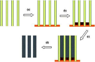 | ||
| Fig. 1 Schematic illustration for synthesizing tin nanowire arrays in AAO membranes: a) sputtering a thick gold layer on the back of AAO membranes; b) electrodeposition of Cu nanorods connected with the gold layer; c) electrodeposition of tin NWs; d) removal of the Au layer, Cu nanorods and AAO membranes. | ||
The geometrical characteristics of the tin nanowires could be controlled by choosing proper types of AAO membranes. A typical sample (sample 1) prepared via the galvanostatic technique is shown in Fig. 2a. Orderly aligned tin nanowire arrays were observed after the AAO template had been partly etched away, suggesting that almost all the pores were filled with tin nanowires. The diameter of the nanowires is ca. 100 nm, in agreement with the diameter of the pores of the selected AAO membrane. After removing the tin NWs and the AAO template, short Cu nanorod arrays with an average vertical length of about 400 nm could be observed on the surface of the gold layer (Fig. 2b).
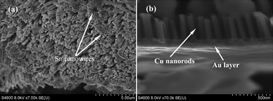 | ||
| Fig. 2 SEM images of a) tin nanowire arrays after the AAO template had been partly etched away and b) copper nanorods connected with the Au layer of sample 1 after removing the tin NWs and the AAO template. | ||
Individual tin nanowires with a length of up to tens of micrometres have been obtained by completely removing the AAO template. TEM characterizations (Fig. 3) demonstrated that the tin nanowires were continuous and uniform in diameter throughout the entire length of the wire. Their average diameter was ca. 100 nm (statistical calculation of fifty nanowires from TEM images). It should be noted that the obtained tin nanowires are sensitive to focused electron beams, and can be melted after exposure for a long time (the marked area in Fig. 3a), demonstrating that the as prepared nanowires have a low melting point, like bulk tin. Nevertheless, the NWs were, in general, stable, and could be characterized by high resolution transmission electron microscopy (HRTEM) techniques.
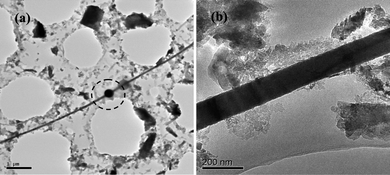 | ||
| Fig. 3 a) A typical TEM image of a single tin nanowire with continuous and uniform diameter at low magnification and b) the high magnification image of part of the tin nanowire shown in a). The marked area in a) shows the melting part of the tin NWs under electron beam exposure for a long time. | ||
A typical HRTEM image of the NWs is shown in Fig. 4. A long range, highly ordered crystalline lattice was observed along the whole length of the NW. The basal distance of the lattice is 0.29 nm, in agreement with the (200) lattice fringes of the tin crystal. The HRTEM and selective area electron diffraction (SAED) analysis (inset of Fig. 4) suggested that tin nanowires with single crystalline structures have been formed, and the single crystal was grown along the [100] direction. It is worthwhile to mention that HRTEM and SAED characterizations have been used to investigate a number of individual tin nanowires. A single set of diffraction spots in the SAED patterns was always obtained on all the investigated NWs, and no grain boundaries were observed along these tin nanowires, indicating that the tin nanowires are essentially single crystalline.
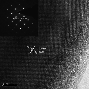 | ||
| Fig. 4 A typical HRTEM image of a tin nanowire in sample 1; the inset is the corresponding selective area electron diffraction (SAED) pattern. | ||
To further investigate the crystalline structure of all the NWs formed in the pores of AAO membrane, X-ray diffraction (XRD) was measured on a piece of AAO membrane containing an array of tin nanowires which was just after electrodeposition and before the removal of the template. A typical XRD pattern obtained from sample 1X (prepared via the same procedure as sample 1) is shown in Fig. 5a. Interestingly, just two peaks were observed and the corresponding 2θ degree of the two peaks fitted very well to the (200) and (400) diffraction peaks of the tin crystal, which could be indexed to the body-centred-tetragonal (bct) β-Sn structure with lattice constants a = b = 5.82 Å; c = 3.17 Å (JCPDF, 4–673). However, for polycrystalline β-tin powder, the ratio of the intensities of the (200) and (101) peaks is expected to be 1.1 (JCPDF, 4–673). This result demonstrated that large scale single crystalline tin nanowire arrays have been formed in the pores of the AAO membrane, and the crystal was grown along the [100] direction, which was in good agreement with the HRTEM and SAED analysis.
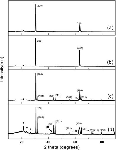 | ||
| Fig. 5 XRD patterns of AAO templates containing an array of tin nanowires fabricated at different electrodeposition conditions: a) sample 1, b) sample 2, c) sample 3 and d) sample 4. The small peak (marked with #) at 2θ = ∼43° corresponds to Cu (111) diffraction from copper nanorods and the peaks (marked with *) in the range of 2θ = 20 ∼ 30° may be due to the existence of a small amount of residue of various metal salts. | ||
The formation of large scale single crystalline tin NWs is closely related to the experimental conditions for electrodeposition. Tin nanowire arrays have been prepared under different electrodeposition conditions as mentioned at the beginning (sample 2, 3, 4). XRD characterizations (Fig. 5b) disclosed that tin nanowires (sample 2) obtained at 2.0 mA cm−2 through galvanostatic technique has almost the same XRD pattern as sample 1, suggesting that the current intensity has little influence on the growth of single crystalline tin nanowires. However, two tin nanowire arrays (sample 3 and 4) obtained via a potentiostatic procedure at different constant potentials both contain polycrystalline structures (Fig. 5c and d), and only the peak intensity ratio of (200)![[thin space (1/6-em)]](https://www.rsc.org/images/entities/char_2009.gif) :(101) could be somehow adjusted through the change of the potential. These results indicate that the use of steady current and lower potential may be beneficial for long range single crystal growth during the electrodeposition.
:(101) could be somehow adjusted through the change of the potential. These results indicate that the use of steady current and lower potential may be beneficial for long range single crystal growth during the electrodeposition.
One possible reason for the growth of single crystalline nanowires may be the formation of 2D-like nucleus under lower overpotential,5 since the smaller the overpotential, the larger the critical dimension of the nucleus, which is favorable for single crystal growth. More importantly, the copper nanorods deposited in the bottom of the AAO nanopores prior to the tin deposition are crucial for large scale single crystal tin NW formation. The growth of tin NW is therefore on the end of the crystalline copper nanorod, instead of polycrystalline Au electrode which may have epitaxial influence on the crystal growth.33 Electrodeposition of tin directly on Au electrode (without copper pre-deposition) through galvanostatic technique resulted in only polycrystalline tin nanowires. To further understand the role of copper nanorods in the high quality tin nanowire formation, the anisotropic structure of the copper nanorods were investigated. With the approach described in this work, we can feasibly control the formation of copper nanorods which has an anisotropic crystalline cross section. The crystalline structures of the individual Cu nanorods were investigated by HREM and SAED experiments (see supporting information, Fig. S1†). Lots of individual Cu nanorods were characterized, and we always observed a single set of diffraction spots in the SAED patterns, indicating that the Cu nanorods were single crystals with a face-centered cubic (fcc) structure. A typical HRTEM image of individual Cu nanorods reveals that the (111) lattice fringes with lattice spacing of around 0.208 nm are approximately vertical to the axis of the nanorod, and that the growth plane is one of the (111) planes. This could be the main reason for the reproducible large scale single crystalline Sn nanowire array formation with this approach. Hence, the crystalline structure of pre-deposited copper nanorods might be in favor of the formation of single crystalline tin structure, for which the mechanism remains to be further investigated in detail.
In summary, we have successfully fabricated single-crystal tin nanowire arrays in large scale with anodic aluminium oxide (AAO) as templates by the electrodeposition method using copper nanorod as a second electrode. The diameter and length of the tin nanowires can be controlled by selecting appropriate AAO membranes. Long and uniform single crystalline tin nanowires have been obtained, and most of the tin nanowires have the obvious preferred orientation along the [100] direction. These high quality single crystalline tin nanowire arrays are expected to be useful in various future applications, including energy storage, sensors, superconductivity, catalysis, and other electronic devices.
Acknowledgements
Financial support from the Chinese Academy of Sciences (KJCX2-YW-M11), the Ministry of Science and Technology of China (2009AA03Z328, 2009DFA41220), and the National Natural Science Foundation of China (20973044) is acknowledged. We thank Dr Manfred Wagner for his help in the preparation of the manuscript.References
- Y. Zhang, G. H. Li, Y. C. Wu, B. Zhang, W. H. Song and L. Zhang, Adv. Mater., 2002, 14, 1227 CrossRef CAS.
- M. L. Tian, J. G. Wang, J. Snyder, J. Kurtz, Y. Liu, P. Schiffer, T. E. Mallouk and M. H. W. Chan, Appl. Phys. Lett., 2003, 83, 1620 CrossRef CAS.
- T. R. Kline, M. L. Tian, J. G. Wang, A. Sen, M. W. H. Chan and T. E. Mallouk, Inorg. Chem., 2006, 45, 7555 CrossRef CAS.
- C. G. Jin, G. W. Jiang, W. F. Liu, W. L. Cai, L. Z. Yao, Z. Yao and X. G. Li, J. Mater. Chem., 2003, 13, 1743 RSC.
- M. L. Tian, J. U. Wang, J. Kurtz, T. E. Mallouk and M. H. W. Chan, Nano Lett., 2003, 3, 919 CrossRef CAS.
- J. G. Wang, M. L. Tian, N. Kumar and T. E. Mallouk, Nano Lett., 2005, 5, 1247 CrossRef CAS.
- Y. Wu, J. Xiang, C. Yang, W. Lu and C. M. Lieber, Nature, 2004, 430, 61 CrossRef CAS.
- M. L. Tian, J. G. Wang, J. S. Kurtz, Y. Liu, M. H. W. Chan, T. S. Mayer and T. E. Mallouk, Phys. Rev. B: Condens. Matter Mater. Phys., 2005, 71, 104521 CrossRef.
- A. Kolmakov, Y. X. Zhang, G. S. Cheng and M. Moskovits, Adv. Mater., 2003, 15, 997 CrossRef CAS.
- L. Shi, Y. M. Xu and Q. Li, Cryst. Growth Des., 2009, 9, 2214 CrossRef CAS.
- L. Shi, Y. M. Xu and Q. Li, J. Phys. Chem. C, 2009, 113, 1795 CrossRef CAS.
- Q. Kuang, C. S. Lao, Z. L. Wang, Z. X. Xie and L. S. Zheng, J. Am. Chem. Soc., 2007, 129, 6070 CrossRef CAS.
- L. Shi, Y. M. Xu, S. K. Hark, Y. Liu, S. Wang, L. M. Peng, K. W. Wong and Q. Li, Nano Lett., 2007, 7, 3559 CrossRef CAS.
- H. D. Liu, Z. X. Ye, H. Zhang, W. H. Wu, Z. P. Luo, K. D. D. Rathnayaka and D. G. Naugle, Phys. B, 2008, 403, 1542 CrossRef CAS.
- G. Yi and W. Schwarzacher, Appl. Phys. Lett., 1999, 74, 1746 CrossRef CAS.
- Y. Idota, T. Kubota, A. Matsufuji, Y. Maekawa and T. Miyasaka, Science, 1997, 276, 1395 CrossRef CAS.
- Q. Zhou, X. Y. Liu, Y. M. Zhao, N. Q. Jia, L. Liu, M. M. Yan and Z. Y. Jiang, Chem. Commun., 2005, 4941 RSC.
- C. K. Chan, H. L. Peng, G. Liu, K. McIlwrath, X. F. Zhang, R. A. Huggins and Y. Cui, Nat. Nanotechnol., 2008, 3, 31 CrossRef CAS.
- L. J. Zhi, J. S. Wu, J. X. Li, M. Stepputat, U. Kolb and K. Mullen, Adv. Mater., 2005, 17, 1492 CrossRef CAS.
- G. L. Cui, L. J. Zhi, A. Thomas, U. Kolb, I. Lieberwirth and K. Mullen, Angew. Chem., Int. Ed., 2007, 46, 3464 CrossRef CAS.
- L. J. Zhi, J. S. Wu, J. X. Li, U. Kolb and K. Mullen, Angew. Chem., Int. Ed., 2005, 44, 2120 CrossRef CAS.
- L. J. Zhi, T. Gorelik, J. S. Wu, U. Kolb and K. Mullen, J. Am. Chem. Soc., 2005, 127, 12792 CrossRef CAS.
- C. R. Martin, Science, 1994, 266, 1961 CrossRef CAS.
- H. Q. Cao, Y. Xu, J. M. Hong, H. B. Liu, G. Yin, B. L. Li, C. Y. Tie and Z. Xu, Adv. Mater., 2001, 13, 1393 CrossRef CAS.
- M. Law, J. Goldberger and P. D. Yang, Annu. Rev. Mater. Res., 2004, 34, 83 CrossRef CAS.
- Z. Miao, D. S. Xu, J. H. Ouyang, G. L. Guo, X. S. Zhao and Y. Q. Tang, Nano Lett., 2002, 2, 717 CrossRef CAS.
- C. C. Chen, Y. Bisrat, Z. P. Lu, R. E. Schaak, C. G. Chao and D. C. Lagoudas, Nanotechnology, 2006, 17, 367 CrossRef CAS.
- H. S. Shin, J. Yu and J. Y. Song, Appl. Phys. Lett., 2007, 91, 173106 CrossRef.
- H. S. Shin, J. Yu, J. Y. Song and H. M. Park, Appl. Phys. Lett., 2009, 94, 011906 CrossRef.
- A. J. Yin, J. Li, W. Jian, A. J. Bennett and J. M. Xu, Appl. Phys. Lett., 2001, 79, 1039 CrossRef CAS.
- H. Masuda, H. Yamada, M. Satoh, H. Asoh, M. Nakao and T. Tamamura, Appl. Phys. Lett., 1997, 71, 2770 CrossRef CAS.
- H. Masuda and K. Fukuda, Science, 1995, 268, 1466 CrossRef CAS.
- H. Pan, H. Sun, C. Poh, Y. P. Feng and J. Y. Lin, Nanotechnology, 2005, 16, 1559 CrossRef CAS.
Footnote |
| † Electronic supplementary information (ESI) available: Experimental details and the information for single crystalline copper nanorods. See DOI: 10.1039/c0nr00206b |
| This journal is © The Royal Society of Chemistry 2010 |