Excitation profile of surface-enhanced Raman scattering in graphene–metal nanoparticle based derivatives†
Xiaoqi
Fu
ab,
Fengli
Bei
a,
Xin
Wang
*a,
Stephen
O'Brien
b and
John R.
Lombardi
*b
aKey Laboratory for Soft Chemistry and Functional Materials (Nanjing University of Science and Technology), Ministry of Education, Nanjing 210094, P. R. China. E-mail: wxin@public1.ptt.js.cn
bDepartment of Chemistry, The City College of New York, New York, N.Y 10031. E-mail: lombardi@sci.ccny.cuny.edu
First published on 4th June 2010
Abstract
Understanding energy transfer mechanisms in graphene derivatives is strongly motivated by the unusually interesting electronic properties of graphene, which can provide a template for the creation of novel nanostructured derivatives. From a synthetic point of view, it is highly attractive to envision being able to synthesize pristine graphene from precursors such as graphene oxide (GO). While this goal may be challenging over large length-scales, it is possible to generate regions of graphene at the nanoscale, confirmed by Raman spectroscopy or other methods. We describe an in situ method of nucleating gold or palladium nanoparticles in the presence of ethylene glycol as a reducing agent, while simultaneously reducing GO to graphene. The Au nanoparticles aid in spectroscopic characterization by both quenching fluorescence, allowing the graphene D and G bands to be quantified, and yielding a surface enhancement of about two orders of magnitude. We observe the excitation profile (488–785 nm) of the surface enhanced Raman spectrum (SERS) of graphene with Au nanoparticles adsorbed on the surface. Both the D and G bands display a resonance at approximately 593 nm (2.09 eV). This resonance may be interpreted as a combination of the plasmon resonance at 548 nm and a likely contribution from charge transfer as well. In addition, we observe a stiffening of the G band compared with that of graphene. The mechanism of the SERS, whether plasmonic or charge transfer-based, enables insight into the electronic pathways available to the graphene–nanoparticle system. We discuss our results in the context of several existing studies of graphene-based nanostructure derivatives.
Introduction
Due to the extraordinary mechanical1 and electronic properties,2 and potential application in sensors,3 integrated circuits,4 catalysis,5,6 ultra capacitors7 and new graphene devices,8 graphene sheets have received intensive attention in recent years. Raman spectroscopy is a powerful technique to provide detailed information as to molecular structures and has proved to be a useful tool to analyze the structure of graphene.9 The most prominent features for graphene in Raman spectra are the G band (around 1582 cm−1 using laser excitation at 2.41 eV) which is associated with the E2g phonon of sp2 atoms, and the D band (around 1350 cm−1) which is due to the breathing mode of κ-point phonons of A1g.10,11 Also often observed is an overtone, the 2D band (some authors prefer to call it the G′ band or D′ band),10,12 which is located at around 2700 cm−1.In general, Raman spectroscopy is limited by its low sensitivity, especially when observing single graphene sheets. Surface enhanced Raman scattering (SERS) is able to overcome this limitation and provide a spectral intensity often enhanced by many orders of magnitude for molecules adsorbed on a properly prepared metal (e.g., Ag, Au) surface. This offers the opportunities for SERS to facilitate the study of graphene sheets in detail. SERS of amorphous carbon,13 fullerenes14 and carbon nanotubes15 has been studied in previous works. SERS on graphene sheets separated from an Ag film by a layer of Al2O3 has been observed at a single excitation wavelength (632.8 nm) by Gao, et al.16 Due to the smooth Ag surface and the separation film, the enhancement factors observed were low. Kneipp17et al. have observed SERS of single-walled carbon nanotubes (SWNTs) in contact with fractal silver colloidal clusters with an enhancement of approximately 12 orders of magnitude. Since graphene sheets have a structure analogous to SWNTs, it is anticipated that a similar SERS effect would be observed.
Recently, members of our research team reported the synthesis of graphene–noble metal composites in a water–ethylene glycol mixture system.18 We found that metal ions could be easily reduced to form metallic nanoparticles (NPs) after adding metallic salts to the mixture of graphene oxide (GO) in the water–ethylene glycol solution, and the resulting metallic NPs played a pivotal role in catalytic reduction of GO with ethylene glycol, and the extent of deoxygenation depended on the attached metals. In this paper, graphene–Au (G-Au) and graphene–Pd (G-Pd) sheets were successfully prepared in the water–ethylene glycol mixture system, and removed to the surface of Si wafer pre-cleaned with ethanol and water. In this way, we obtained high quality SERS spectra from G-Au and G-Pd sheets. By varying the excitation wavelength of lasers, we obtained the SERS excitation profile of G-Au. For comparison, we have also obtained data for G-Pd.
Experimental section
Chemicals
Gold chloride trihydrate (HAuCl4·3H2O) and potassium tetrachloropalladate (K2PdCl4) were purchased from Sigma-Aldrich Co. Natural graphite powder (44 μm) was provided by Qingdao Zhongtian Company. The other chemicals were all analytical grade without further purification.Sample preparation
GO was prepared according to the method reported by Hummers and Offeman.19 Graphene–metal particle nanocomposites were synthesized according to the method reported by members of our research team.18 10 mg of the obtained graphite oxide powder was dispersed in 10 mL of water by sonication, forming stable graphene oxide colloid. After 1 h, metal precursor (HAuCl4·3H2O and K2PdCl4) was dissolved in water to obtain 0.01 M solution. 0.5 mL of the resulting metal salt solution and 20 mL of ethylene glycol were added to the graphene oxide colloid solution with magnetic stirring for 30 min. Subsequently, the mixture was heated to 100 °C and aged at that temperature for 6 h. The bulk samples can be obtained by centrifugation of the mixture, and then washing with deionized water and ethanol several times. Brown colored G-Au and black colored G-Pd were obtained after the precipitate was dried at 60 °C under vacuum for 12 h. It should be noted that graphene oxide is quite stable in ethylene glycol solution without adding metallic salts. This is because Au and Pd NPs can be easily obtained by reduction of the corresponding metallic salt in ethylene glycol, and the obtained NPs play important roles as catalysts in the reduction of graphene oxide with ethylene glycol. The oxidation potential at a carbon electrode for ethylene glycol (1.65 V/SCE) is greater than the reduction potential for both AuCl4− (0.62 V/SCE)20 and graphene oxide, so that there is adequate energy with which to reduce both graphene oxide and Au3+.Sample characterization
X-Ray diffraction (XRD) patterns of G-Au and G-Pd were recorded on a Bruker D8 Advanced X-ray diffractometer using Cu-Kα radiation (λ = 0.1542 nm). The morphologies of samples were observed by transmission electron microscope (TEM, JEM-2100) and scanning electron microscope (SEM, JSM-6380LV) equipped with an energy dispersive X-ray spectrometer (EDS). The electronic absorption spectra were recorded on a Shimadzu UV-1201 UV-vis spectrophotometer with standard 1 cm optical path quartz cells. The Raman spectra of samples were investigated at the excitation wavelengths of 488.0 and 514.5 nm obtained from an Ar+ laser (Spectra Physics), at 632.8 nm obtained from a He/Ne laser (Melles Griot), and at 785 nm obtained from a Kr+ laser (Spectra Physics). To ensure the obtained spectra were comparable, the settings, including the lasers’ power and exposure time, were all the same. The silicon line at 520 nm was used to calibrate the observed wavenumbers and adjust the intensities by comparing them with the absolute intensities of Si obtained by Renucci et al.21Results and discussion
We describe our material samples as graphene–metal nanoparticle derivatives, G-Au and G-Pd, prepared from the simultaneous, in situ reduction of Au and Pd molecular precursors in the presence of Graphene Oxide (GO). X-Ray powder diffraction patterns of the resulting G-Au and G-Pd, as well as that of GO, are shown in Fig. 1. The diffraction peak at around 2θ = 10°, corresponding to the (001) reflection of GO, almost disappears in the pattern of G-Au and G-Pd. The other peaks are all ascribed to the characteristic Bragg reflections of gold22 and palladium,23 respectively, indicating that the regular layer structures of GO or graphene are disrupted and the Au or Pd NPs were formed and attached to its surface. The morphologies of the obtained samples can be seen from electron microscope images. Fig. 2 shows the TEM images of G-Au and G-Pd. It is clearly seen that most metal NPs distribute randomly on the sheets. Although there are some large triangular gold particles on the sheets, most particles are nanospheres. The metal salts can be easily reduced in the water–ethylene glycol solution, and the resulting metal NPs can grow in situ on the defects originating from the oxygenation of graphite by strong oxidants.18 This can be verified by the SEM and EDS images (Fig. 3). It is clearly seen that the sheets become more corrugated after the attachment of metal NPs. The upper inset EDS images show that G-Au and G-Pd contain the element Au and Pd, respectively, apart from the initial C and O. Additionally, the ratio of the contents (O/C) is somewhat lower compared to that of GO, which reveals that these metal NPs play some important roles, and most probably act as catalysts, in the reduction of graphene oxide with ethylene glycol, and the extent of deoxygenation depends on the attached metals.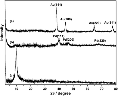 | ||
| Fig. 1 XRD pattern of the resulting (a) G-Au, (b) G-Pd and (c) GO. | ||
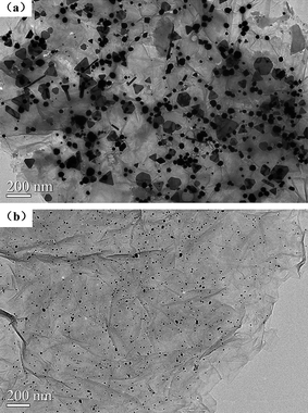 | ||
| Fig. 2 TEM images of (a) G-Au and (b) G-Pd. | ||
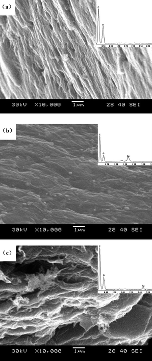 | ||
| Fig. 3 SEM images of (a) graphite oxide, (b) G-Au and (c) G-Pd. The insets are EDS images. | ||
Absorption spectra were obtained in order to investigate the effect of attaching metal NPs onto GO sheets. Fig. 4 shows the spectra of G-Au, G-Pd and GO sheets dispersed in aqueous solution. As Fig. 4c shows, the characteristic absorption peak of aqueous GO solution at 229 nm red shifted to 259 nm, due to the deoxygenation of GO. Another band around 548 nm may be ascribed to the gold plasmon absorption.24 The spectrum of G-Pd also shows a red shift to 240 nm, but there is no trace of the palladium plasmon absorption peak.
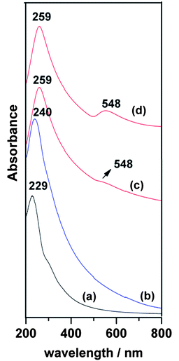 | ||
| Fig. 4 Absorption spectra of (a) GO dispersed in aqueous solution, (b) G-Pd and (c) G-Au, (d) G-Au at higher Au concentration. | ||
In order to record the Raman spectra of G-Au and G-Pd, an aliquot of 10 μL of G-Au or G-Pd dispersion was dropped onto a Si wafer. The Si wafer was dried at 60 °C under vacuum overnight and measured in air. In Fig. 5, we show the Raman spectra of G-Au at different excitation wavelengths, together with the normal Raman spectrum of GO sheets. To the right of the Raman spectra, we show the images of G-Au and GO on the Si wafer that were observed under Raman microscopy and taken for the Raman measurements. The sheets of G-Au and GO appear to be one or two layers on the Si wafer, and the sheets became smaller after reaction with gold chloridetrihydrate in water–ethylene glycol solution.
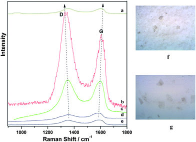 | ||
| Fig. 5 Raman spectra of G-Au at excitation wavelengths of (a) 785, (b) 632.8, (c) 514.5 and (d) 488 nm, and Raman spectrum of (e) GO at 488 nm. On the right, the images of (f) G-Au (top) and (g) GO (bottom) on the Si wafer that were observed under Raman microscopy and taken for the Raman measurements. | ||
The Raman spectrum (Fig. 5e) of GO shows the well-known main groups of bands: the tangential stretching mode of the E2g phonon of sp2 atoms (G band) in the range of 1500–1600 cm−1, as well as the breathing mode of κ-point phonons of A1g (D band) in the range of 1200–1500 cm−1. The corresponding band positions and vibrational assignments are listed in Table 1. The Raman spectrum of G-Au at 488 nm, also contains both D and G bands, however, with an increased D/G intensity ratio compared to that in GO. In Fig. 5d (at 488 nm), the intensity of the Raman spectrum of G-Au is enhanced somewhat compared to that of GO sheets (Fig. 5e). Specifically, the ratio of intensities of the D band to that of the G band (ID/IG) decreases from approximately 1 for GO to about 0.75 for the reduced sample. This observation is consistent with the Tuinstra–Koenig relationship which correlates a decrease in this ratio to an increase in La, the conjugation length of sp2 rings.25 This makes sense with respect to the formation of more extended networks of conjugated sp2 carbons, towards a more locally ordered graphene lattice. In addition, Fig. 5 indicates that at different wavelengths, the intensity of the D band was enhanced about 5 times when we measured with 514.5 nm excitation wavelength compared to that of GO, and 27 times for 632.8 nm excitation wavelength. For the G band, the intensity is enhanced by a factor of 3 for 514.5 nm and 16 for 632.8 nm excitation, respectively, compared to that of GO. However, the enhancement decreased considerably when the excitation wavelength is changed to 785 nm. In Fig. 6, we provide an excitation profile of the D and G bands. Note that this profile indicates a resonance. A Gaussian fit to the D band profile gives a maximum of 2.09 eV (593 nm) and a width of 0.30 eV. See the ESI Fig. S1 for the details of this fit.†
| Band | Graphene at 488 nm | G-Au at 488 nm | G-Au at 514.5 nm | G-Au at 632.8 nm | G-Au at 785 nm |
|---|---|---|---|---|---|
| D band | 1350 | 1357.7 | 1348.6 | 1330.9 | 1350.9 |
| G band | 1582 | 1583.7 | 1599.5 | 1605.0 | 1602.5 |
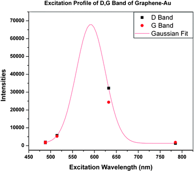 | ||
| Fig. 6 Excitation profile of the D (■) and G (●) bands of graphene enhanced with Au nanoparticles. | ||
In the ESI, Fig. S2 also contains a few SERS spectra of G-Pd.† From Fig. 4b, we see that there is no intense plasmon resonance contribution to the absorption spectrum of G-Pd, and the SERS spectra observed for this system are considerably weaker than those for G-Au. For this reason, in this paper we have focused mainly on the latter results.
It is generally accepted that two mechanisms contribute to the surface enhancement: the electromagnetic (EM) and the charge transfer (CT) mechanisms. Additional enhancement can also be obtained from molecular resonances, but they are not likely in the system considered here. The former is a result of the large increase of the local electric field caused by surface plasmon resonances (SPR) of nanosized metals.26 The EM enhancement usually can contribute factors of about 104–106 to the Raman enhancement,27 even about 1014-fold in some single molecule studies.28,29 The CT enhancement involves the chemisorption interaction and the metal–adsorbate charge transfer, and is usually said to contribute factors of about 10–100 of the observed enhancement.30,31 At a CT resonance, however, a considerably larger fraction of the enhanced intensity can be contributed.32 Although it is often thought that the two mechanisms are independent, it has recently been shown that they are intimately linked,33 but one or the other might dominate at a given excitation wavelength. This demonstrates the importance of good excitation profiles in interpreting the results of SERS.
The plasmon resonance of Au is in the vicinity of 548 nm (Fig. 4b), at some distance from the excitation profile maximum of about 593 nm. Aggregation of metal nanoparticles can result in a red shift of the plasmon resonance. Although the TEM images show a significant fraction of larger nanoparticles, we see little shift in the absorption spectrum, nor any other significant maximum besides that at 548 nm, even at higher concentrations (Fig. 4a). It is common in SERS to observe a difference between the plasmon resonance and the maximum of the excitation profile. For example, Yamada et al. found in pyridine on Ag films that the peaks diverged considerably.34 The plasmon resonance of the Ag film was at 490 nm, while the excitation profile peaked at 590 nm. This is similar to Seki’s results on a Ag electrode.35 Hildebrandt and Stockburger found a similar effect in Rhodamine 6-G,36 where the plasmon resonance is at about 420 nm and the excitation profile maximum is about 530 nm. In these and many other cases, the difference was attributed to contributions from charge transfer transitions between the molecule and metal. Charge transfer between carbon nanotubes and Au(111) has been observed by Wildöer et al.37 Since the work function of Au is −5.3 eV (relative to the vacuum level) and that of graphite (presumably close to that of the nanotubes) is −4.5 eV, they expect easy charge transfer from the nanotubes to the metal. They show that the Fermi level shifts toward the valence band of the nanotubes.
SERS has also been observed for Ag–PATP–graphene and graphene oxide. The molecule PATP (p-aminothiophenol) is often used as a test for charge transfer effects since the non-totally symmetric b2 modes tend to dominate the spectrum during charge transfer processes, while the totally symmetric a1 modes predominate when far from charge transfer conditions. Zhou et al.38 observed extremely large enhancements of the b2 modes relative to the a1 modes, indicating very large charge transfer in such a system. Note that their excitation wavelength (488 nm) is in the region of charge transfer bands in the PATP–Ag system.
Voggu et al.,39 using both a strong electron donor (tetrathiafulvalene, TTF) and a strong electron acceptor (tetracyanoethylene, TCNE), showed that as the concentration of each in a solution of graphene increases, the G band either softens (with TTF) or stiffens (with TCNE). In Table 1 we show the stiffening of the G band for all excitation energies (as compared to the value of 1582 cm−1 for pure graphene), and by analogy with the Voggu results, we may infer that the direction of ground state charge transfer is from the graphene to the Au nanoparticles. This is consistent with the difference in work functions. Note that Voggu et al. also observed charge transfer bands in the visible spectrum of graphene–TTF and graphene–TCNE. They identify the bands which have peaks at around 590 nm for TTF and 580 nm for TCNE. This is exactly in the range of the resonance we observe at 593 nm.
Additional evidence for charge transfer (sometimes called chemical enhancement) effects is presented by Jasuja and Berry,40 who show that both the D and G band are enhanced by up to 800% by increasing the dendritic growth of Au nanoparticles on graphene derivatives. Their experiments further suggest a Shottky barrier between the metal and graphene nanostructure. The estimated Shottky barrier height for the Au–graphene junction is 39 meV. At room temperature (kT = 22 meV), therefore, we would expect that the graphene–gold system can equilibrate by means of charge transfer from the graphene to the metal.
In Fig. S3 of the ESI,† we show the Raman spectra of a sample of pure graphene with Au nanoparticles dropped on. Note the lack of resonant enhancement, the lack of dispersion with excitation wavelength, and the lack any intensity in the D band. These results are typical of uniform and ordered films of exfoliated graphene. This is in considerable contrast to the results shown in Fig. 5, and illustrates the difference to the sample discussed here, in which there is a clear resonance with excitation wavelength. The sample was made starting with graphene oxide, and the reduction of Au was carried out in situ. The resulting sample has considerable disorder, as shown by the prominent D band as well as the G band dispersion. It is clear that the results displayed in Fig. 5 show a considerable SERS enhancement, and that the method of growth results in a stronger bond with the graphene surface, resulting in a lower Shottky barrier. This facilitates a better interaction of the Au nanoparticles with the surface, and more facile equilibration of the Fermi levels of both components of the system. The result is that charge transfer is facilitated in this system, despite the increased disorder.
In Table 1, we present the effect of varying the excitation wavelength on the G band wavenumbers. Note that the band stiffens at all excitation energies, from 1582 cm−1 at 2.54 eV, to as much as 1605 cm−1 at 1.58 eV. Stiffening of the G band is a characteristic of disordered graphitic systems (as is the D band). It is not observed for highly ordered systems. This has been extensively discussed by Ferrari and Robertson,41 as being due to resonant selection of disordered sp2 configurations with wider π gaps. This increased gap results from higher degrees of disorder, and therefore higher vibrational frequencies. By applying gate modulated charge density, Yan et al.42 examined the effect of charge or hole injection on electron–phonon coupling in single layer graphene. Using Raman excitation at 488 nm, they showed that for both n-type and p-type doping, the G band stiffens, from 1584 cm−1 at the zero point to 1594 cm−1 at a Fermi level shift of 300 meV. They interpret their results to indicate that electron–phonon coupling is important in wavenumber shifts observed in graphene. Das et al.43 found a similar result by varying the doping level in electrochemical top-gated graphene transistors. They found that injecting either holes or electrons had the effect of stiffening the G band wavenumber at 514.5 nm excitation. In their results the G band stiffened from 1584 cm−1 to over 1605 cm−1 using increasing electron or hole concentrations to change the Fermi energy from 0 to ±700 meV.
Conclusion
We have investigated the SERS excitation profile for graphene with Au nanoparticles attached. The profile shows a resonance at around 2.09 eV, in both the G band and D band vibrations. Since this does not coincide with the plasmon resonance in Au, we take it to represent additional charge transfer contributions to the enhancement. Analysis of the stiffening of the G band indicates the importance of electron–phonon coupling in the G band spectrum, and helps define the degree of charge transfer in the ground state of the Au–graphene complex.Acknowledgements
We wish to thank Prof. Zhonghua Yu and Mr Yi Pan for valuable help in carrying out this project. We also thank Prof. Tony Heinz and Leandro Malard for critical comments concerning the manuscript. SO and XF are indebted to Mr Zhang Jia and Inanc Meric for help with providing samples of exfoliated graphene. The work was supported by the National Natural Science Foundation of China (No. 10776014, No. 50772048) and the High-Tech Foundation of Jiangsu Province, China (BG2007047). We are also indebted to the National Institute of Justice (Department of Justice award No. 2006-DN-BX-K034) and the City University Collaborative Incentive program (No. 80209). This work was also supported by the National Science Foundation under cooperative agreement No. RII-9353488, grants No. CHE-0091362, CHE-0345987, and No. ECS0217646. Additional support was provided by the City University of New York PSC-BHE Faculty Research Award Program.References
- C. Lee, X. Wei, J. W. Kysar and J. Hone, Science, 2008, 321, 385 CrossRef CAS.
- P. Avouris, Z. Chen and V. Perebeinos, Nat. Nanotechnol., 2007, 2, 605 CrossRef CAS.
- F. Schedin, A. K. Geim, S. V. Morozov, E. W. Hill, P. Blake, M. I. Katsnelson and K. S. Novoselov, Nat. Mater., 2007, 6, 652 CrossRef CAS.
- J. Chen, M. Ishigami, C. Jang, D. R. Hines, M. S. Fuhrer and E. D. Williams, Adv. Mater., 2007, 19, 3623 CrossRef CAS.
- K. Jasuja and V. Berry, ACS Nano, 2009, 3, 2358 CrossRef CAS.
- Y. C. Si and E. T. Samulski, Chem. Mater., 2008, 20, 6792 CrossRef CAS.
- M. D. Stoller, S. Park, Y. Zhu, J. An and R. S. Ruoff, Nano Lett., 2008, 8, 3498 CrossRef CAS.
- T. J. Echtermeyer, M. C. Lemme, M. Baus, B. N. Szafranek, A. K. Geim and H. Kurz, IEEE Electron Device Lett., 2008, 29, 952 CrossRef CAS.
- K. N. Kudin, B. Ozbas, H. C. Schniepp, R. K. Prud'homme, I. A. Aksay and R. Car, Nano Lett., 2008, 8, 36 CrossRef CAS.
- L. M. Malard, D. L. Mafra, S. K. Doorn and M. A. Pimenta, Solid State Commun., 2009, 149, 1136 CrossRef CAS.
- L. M. Malard, M. A. Pimenta, G. Dresselhaus and M. S. Dresselhaus, Phys. Rep., 2009, 473, 51 CrossRef CAS.
- D. Graf, F. Molitor, K. Ensslin, C. Stampfer, A. Jungen, C. Hierold and L. Wirtz, Nano Lett., 2007, 7, 238 CrossRef.
- M. Veres, M. Fule, S. Toth, M. Koos and I. Pocsik, Diamond Relat. Mater., 2004, 13, 1412 CrossRef CAS.
- G. G. Siu, Y. L. Liu, S. S. Xie, J. M. Xu, T. K. Li and L. G. Xu, Thin Solid Films, 1996, 274, 147 CrossRef CAS.
- S. Lefrant, Curr. Appl. Phys., 2002, 2, 479 CrossRef.
- L. Gao, W. Ren, B. Liu, R. Saito, Z. S. Wu, S. Li, C. Jiang, F. Li and H. M. Cheng, ACS Nano, 2009, 3, 933 CrossRef CAS.
- K. Kneipp, H. Kneipp, P. Corio, S. D. M. Brown, K. Shafer, J. Motz, L. T. Perelman, E. B. Hanlon, A. Marucci, G. Dresselhaus and M. S. Dresselhaus, Phys. Rev. Lett., 2000, 84, 3470 CrossRef CAS.
- C. Xu, X. Wang and J. Zhu, J. Phys. Chem. C, 2008, 112, 19841 CrossRef CAS.
- W. S. Hummers and R. E. Offeman, J. Am. Chem. Soc., 1958, 80, 1339 CrossRef CAS.
- F. Bonet, C. Guery, D. Guymond, R. Herrera Urbina, K. Tekaia-Elhsissen and J.-M. Tarascon, Int. J. Inorg. Mater., 1999, 1, 47–51 CrossRef CAS.
- J. B. Renucci, R. N. Tyte and M. Cardona, Phys. Rev. B: Solid State, 1975, 11, 3885 CrossRef CAS.
- Y. Luo, Mater. Lett., 2006, 60, 3361 CrossRef CAS.
- C. C. Wang, D. H. Chen and T. C. Huang, Colloids Surf., A, 2001, 189, 145 CrossRef CAS.
- T. Cassagneau and J. H. Fendler, J. Phys. Chem. B, 1999, 103, 1789 CrossRef CAS.
- G. Abrasonis, R. Gago, M. Vinnichenko, U. Kreissig, A. Kolitsch and W. Moller, Phys. Rev. B, 2006, 73, 125427 CrossRef.
- M. Moskovits and J. S. Suh, J. Phys. Chem., 1984, 88, 5526 CrossRef CAS.
- S. J. Lee, A. R. Morrill and M. Moskovits, J. Am. Chem. Soc., 2006, 128, 2200 CrossRef CAS.
- S. M. Nie and S. R. Emory, Science, 1997, 275, 1102 CrossRef CAS.
- K. Kneipp, Y. Wang, H. Kneipp, L. T. Perelman, I. Itzkan, R. R. Dasari and M. S. Feld, Phys. Rev. Lett., 1997, 78, 1667 CrossRef CAS.
- J. R. Lombardi, R. L. Birke, L. A. Sanchez, I. Bernard and S. C. Sun, Chem. Phys. Lett., 1984, 104, 240 CrossRef CAS.
- J. R. Lombardi, R. L. Birke, T. Lu and J. Xu, J. Chem. Phys., 1986, 84, 4174 CrossRef CAS.
- M. Osawa, N. Matsuda, K. Yoshii and I. Uchida, J. Phys. Chem., 1994, 98, 12702 CrossRef CAS.
- J. R. Lombardi and R. L. Birke, J. Phys. Chem. C, 2008, 112, 5605 CrossRef CAS.
- H. Yamada, H. Nagata, K. Toba and Y. Nakao, Surf. Sci., 1987, 182, 269 CrossRef CAS.
- H. Seki, J. Electroanal. Chem., 1983, 150, 425 CAS.
- P. Hildebrandt and M. Stockburger, J. Phys. Chem., 1984, 88, 5935 CrossRef CAS.
- J. W. G. Wildöer, L. C. Venema, A. G. Rinzler, R. E. Smalley and C. Dekker, Nature, 1998, 391, 59 CrossRef CAS.
- X. Zhou, X. Huang, X. Qi, S. Wu, C. Xue, F. Y. C. Boey, Q. Yan, P. Chen and H. Zhang, J. Phys. Chem. C, 2009, 113, 10842 CrossRef CAS.
- R. Voggu, B. Das, C. S. Rout and C. N. R. Rao, J. Phys.: Condens. Matter, 2008, 20, 472204 CrossRef.
- K. Jasuja and V. Berry, ACS Nano, 2009, 3, 2358 CrossRef CAS.
- A. C. Ferrari and J. Robertson, Phys. Rev. B: Condens. Matter Mater. Phys., 2001, 64, 075414 CrossRef.
- J. Yan, Y. Zhang, P. Kim and A. Pinczuk, Phys. Rev. Lett., 2007, 98, 166802 CrossRef.
- A. Das, S. Pisana, B. Chakreborty, S. Piscanec, S. K. Saha, U. V. Waghmare, K. S. Novoselov, H. R. Krishnamurthy, A. K. Geim, A. C. Ferrari and A. K. Sood, Nat. Nanotechnol., 2008, 3, 210 CrossRef CAS.
Footnote |
| † Electronic supplementary information (ESI) available: Details of the Gaussian fit to the excitation profile, and SERS spectra of G-Pd. See DOI: 10.1039/c0nr00135j |
| This journal is © The Royal Society of Chemistry 2010 |