3D ordered nanostructures fabricated by nanosphere lithography using an organometallic etch mask
Xing Yi
Ling†
a,
Canet
Acikgoz†
ab,
In Yee
Phang
b,
Mark A.
Hempenius
b,
David N.
Reinhoudt
a,
G. Julius
Vancso
*b and
Jurriaan
Huskens
*a
aMolecular Nanofabrication Group, MESA+ Institute for Nanotechnology, University of Twente, P.O. Box 217, 7500 AE, Enschede, The Netherlands. E-mail: j.huskens@utwente.nl
bMaterials Science and Technology of Polymers, MESA+ Institute for Nanotechnology, University of Twente, P.O. Box 217, 7500 AE, Enschede, The Netherlands. E-mail: g.j.vancso@utwente.nl
First published on 27th May 2010
Abstract
A new approach for fabricating porous structures on silicon substrates and on polymer surfaces, using colloidal particle arrays with a polymer mask of a highly etch-resistant organometallic polymer, is demonstrated. Monolayers of silica particles, with diameters of 60 nm, 150 nm, 300 nm, or 500 nm, were deposited either on a silicon substrate or on a surface coated with polyethersulfone (PES), and the voids of the arrays were filled with poly(ferrocenylmethylphenylsilane) (PFMPS). Argon ion sputtering removed the excess PFMPS on the particles which enabled removal of the particles with HF. Further pattern transfer steps with reactive ion etching for different time intervals provided structures in silicon or in a PES layer. Free-standing PES membranes exhibiting regular arrays of circular holes with high porosity were fabricated by using cellulose acetate as a sacrificial layer. The pores obtained on silicon substrates after etching were used as molds for nanoimprint lithography (NIL). A combination of the techniques of nanosphere lithography (NSL) and NIL has resulted in 3D nanostructures with a hemispherical shape (inherited from the nanoparticles) which was obtained both in silicon and in PMMA.
Introduction
Nanotechnology requires approaches to control the structure of matter down to the nm length scale for the fabrication of the future generations of optical, electronic and biological devices.1 In particular, nanofabrication opens the door for the increasing demand of miniaturization owing to its ability to design and manufacture structures.Conventional lithographies, e.g. photolithography, e-beam lithography, X-ray lithography, and ion-beam lithography, although suitable for the fabrication of nanometre-sized structures, are often expensive with high capital and running costs.2 As a result, alternative and unconventional techniques, e.g. soft lithography, nanoimprint lithography, scanning probe lithography and self-assembly have been developed in recent years to fulfil the needs for cheap and user-friendly fabrication techniques, in particular for use in research environments where rapid prototyping and versatility are crucial. Microcontact printing3 has been demonstrated to produce self-assembled structures with high yield. However, because of the elastomeric properties of the PDMS stamp, it is difficult to fabricate structures with sub-micron dimensions.3 Nanoimprint lithography, pioneered by Chou et al. has emerged as a good candidate for the fabrication of structures with nanometre scale dimensions.4,5 By applying a prefabricated master (or mold) onto a thin film of polymer above the glass transition temperature and at high pressure, structures are replicated by flow of the polymer into the mold features. For nanostructures, the fabrication of the mold is usually the bottleneck of this technique.
Nanosphere lithography (NSL) employs self-assembled single or double layers of particles as lithographic masks or templates to produce nanosized features of polymers and metals in a low cost and simple manner.6–8 Complex equipment is not required to create patterns on the nanometre scale and the assembly of the particles is achieved readily by spin-coating or dip-coating. In most examples of NSL, particles are assembled into arrays in order to serve as templates, the voids of which are infiltrated by a material that solidifies therein. To fill the voids, a range of materials can be used employing various routes such as chemical vapor deposition, liquid-phase reactions, deposition of small particles and sol–gel chemistry.9–11 Long-range periodic structures such as honeycomb lattices,12 hexagonally packed nanoparticle arrays and nano-triangles13 have been obtained on diverse substrates such as graphite and diamond,14 and polymers15 after subsequent removal of the particles. Various ordered 1D nanostructure arrays, consisting of carbon nanotubes,16 ZnO nanorods17 and Si nanorods18 have been produced by using nanoparticle arrays as the template. The use of such nanoparticle arrays as masks for silicon etching has resulted in silicon pillars which are important for semiconductor technology.19
Spherical colloidal particles can be utilized also for preparing various types of porous materials that exhibit precisely controlled pore sizes and highly ordered 3D porous structures. After drying the colloidal array, the void spaces among the colloidal spheres are fully infiltrated with a liquid precursor such as an ultraviolet (UV)20 or thermally curable organic prepolymer,21 or an ordinary organic monomer (plus an initiator).22 Infiltration into the voids with poly(ferrocenylmethylphenylsilane) (PFMPS) to function as an etch resist to fabricate highly ordered, well defined pore size polymeric membranes has recently been demonstrated by our group.23 Poly(ferrocenylsilanes) (PFS)24,25 owe many of their useful and unique characteristics to the presence of ferrocene and silane units in the main chain which, upon exposure to oxygen plasma, lead to the formation of a silicon/iron oxide layer at the surface since the inorganic components are converted into nonvolatile oxides which are inert to further etching.26,27 In our previous work, we followed a multilayer fabrication strategy with the aim of preparing porous polyethersulfone (PES) on silicon substrates by using the etch resistivity of PFMPS. In contrast to regular NSL, in our case the silica particles were not used as an etch mask, but rather as an inversion mask. Here we present the fabrication of PES membranes with different pore sizes. In addition, we show a simple and versatile approach to pattern silicon substrates by using NSL-prepared patterned PFMPS layers as an etch mask. The high etch resistivity of PFMPS is critically important in this process since the polymeric patterns formed are transferred down to the substrate in a single step using reactive ion etching (RIE). Other polymeric materials can break down more easily when exposed to reactive ion species during RIE processing, and in many cases pattern transfer is only achieved by metal evaporation and lift-off processes. The use of PFMPS eliminates these steps by directly providing a sufficiently high etch resistivity. The fabrication of 3D patterns into a silicon substrate with controlled shape is accomplished owing to the etch resistivity of PFMPS. The size of the pores is tuned by varying the etching time. Large-scale periodic structures with hemispherical shape are fabricated and these are used as a mold for NIL to imprint PMMA.
Experimental
Materials
Silica nanoparticles were purchased from Polysciences Inc. (diameter = 500 nm, 300 nm, 150 nm, standard deviation <10%) as an aqueous suspension, particles of 60 nm were synthesized following a literature procedure.28 1H,1H,2H,2H-perfluorodecyltriethoxysilane (PFDTS, ABCR) and poly(methyl methacrylate) (PMMA, Mw ∼ 35,000 g mol−1, Acros) were used as received.Polymer synthesis
[1]Methylphenylsilaferrocenophane was prepared as described before.24,29 The monomer was purified by several crystallizations from n-heptane at −70 °C followed by vacuum sublimation. Transition metal-catalyzed ring-opening polymerization of [1]methylphenylsilaferrocenophane was carried out in the presence of Et3SiH with the addition of Karstedt's catalyst. The poly(ferrocenylmethylphenylsilane)(PFMPS) was then precipitated in n-heptane. The weight average and number average molar masses Mw and Mn of the polymer were determined by gel permeation chromatography (GPC) measurements in THF, using polystyrene calibration, Mw = 5.5 × 10⁴ g mol−1, Mn = 5.1 × 10⁴ g mol−1, Mw/Mn = 1.09.Substrate preparation
Silicon substrates were cleaned by immersion in piranha solution (conc. H2SO4 and 33% aq H2O2 in a 3![[thin space (1/6-em)]](https://www.rsc.org/images/entities/char_2009.gif) :1 volume ratio, Warning!Piranha should be handled with caution; it can detonate unexpectedly) for 15 min to form a SiO2 layer of 1.5 nm on the surface. The formed SiO2 layer increases the surface hydrophilicity to assist the assembly of particles onto the surface via capillary forces. The substrates were then sonicated in Milli-Q water and ethanol for 1 min, and dried with N2. A monolayer of silica particles on the silicon substrate was prepared by vertical capillary assisted deposition at a withdrawal speed of 0.5 μm s−1.30 A layer of 80 nm of PFMPS was spin-coated onto the particle layer from a 2 wt% PFMPS solution in toluene. The top layer of PFMPS was etched away by argon plasma sputtering for 25 min (Ion Beam Etcher, 350 V, 6 mA) resulting in exposure of the top of the silica particle arrays. The silica particles were removed by dipping the substrate into a 10 wt% aqueous hydrogen fluoride (HF) solution for 12 h, followed by rinsing with Milli-Q water and drying with N2. (Warning! HF solution should be handled with caution; it can cause serious health problems.) Reactive ion etching (RIE) experiments were performed in a reactive ion etching setup, carried out in an Elektrotech PF 340 apparatus (10 mTorr, 20 sccm O2 and 40 sccm SF6, 50W). Substrates were dipped in 10 wt% aqueous nitric acid solution to remove oxidized (PFMPS) from the substrate. Subsequently, an anti-sticking layer of PFDTS was applied.
:1 volume ratio, Warning!Piranha should be handled with caution; it can detonate unexpectedly) for 15 min to form a SiO2 layer of 1.5 nm on the surface. The formed SiO2 layer increases the surface hydrophilicity to assist the assembly of particles onto the surface via capillary forces. The substrates were then sonicated in Milli-Q water and ethanol for 1 min, and dried with N2. A monolayer of silica particles on the silicon substrate was prepared by vertical capillary assisted deposition at a withdrawal speed of 0.5 μm s−1.30 A layer of 80 nm of PFMPS was spin-coated onto the particle layer from a 2 wt% PFMPS solution in toluene. The top layer of PFMPS was etched away by argon plasma sputtering for 25 min (Ion Beam Etcher, 350 V, 6 mA) resulting in exposure of the top of the silica particle arrays. The silica particles were removed by dipping the substrate into a 10 wt% aqueous hydrogen fluoride (HF) solution for 12 h, followed by rinsing with Milli-Q water and drying with N2. (Warning! HF solution should be handled with caution; it can cause serious health problems.) Reactive ion etching (RIE) experiments were performed in a reactive ion etching setup, carried out in an Elektrotech PF 340 apparatus (10 mTorr, 20 sccm O2 and 40 sccm SF6, 50W). Substrates were dipped in 10 wt% aqueous nitric acid solution to remove oxidized (PFMPS) from the substrate. Subsequently, an anti-sticking layer of PFDTS was applied.
Nanoimprint lithography
A piranha-cleaned silicon substrate was first spin-coated with a 500 nm thick layer of poly(methyl methacrylate) (PMMA). Stamp and substrate were put in contact and a pressure of 20 bar was applied at a temperature of 200 °C using a hydraulic press (Specac).All SEM images were taken with a HR-LEO 1550 FEF SEM. The samples were not coated with a conducting layer. AFM measurements were carried out with a Dimension D3100 using a NanoScope IVa controller equipped with a hybrid 153 scanner (Veeco/Digital Instruments (DI), Santa Barbara, CA) under ambient conditions. Silicon cantilevers from Nanosensors (Nanosensors, Wetzlar, Germany) were used for intermittent contact (tapping) mode operation.
Results and discussion
Fig. 1 displays the fabrication procedure that is used to prepare 3D nanostructures on a PES-coated silicon substrate (Fig. 1A) and on a silicon substrate (Fig. 1B). In general, the process starts with the convective assembly of a nanoparticle array onto a substrate followed by spin coating with PFMPS, followed by an etch sequence for transferring the patterns into the Si substrate or into a PES polymer layer. To fabricate a positive replica of the nanoparticle array, the fabricated Si structure is used as a mold for NIL.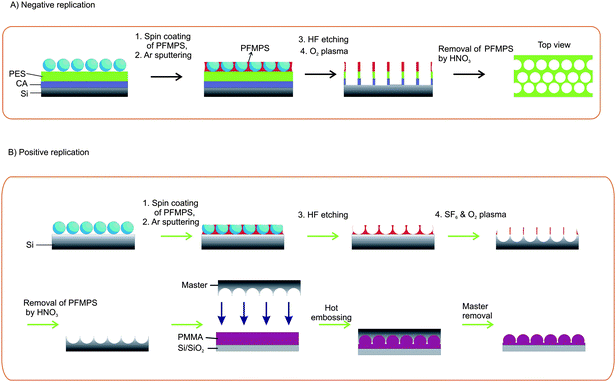 | ||
| Fig. 1 Fabrication scheme for (A) free-standing PES membranes, and (B) patterned silicon substrates by the convective assembly of nanoparticles onto a substrate followed by spin coating of PFMPS, followed by etch steps for transferring the patterns into a PES polymer layer or into the Si substrate. | ||
The combination of nanosphere lithography (NSL) and a mask transfer technique using 300 nm silica particles allowed the fabrication of uniform, nanoporous PES membranes (Fig. 1A).23 First a sacrificial cellulose acetate31 layer is spin-coated on a silicon substrate followed by spin coating of PES. After the assembly of silica nanoparticles by the convective assembly method, PFMPS is spin-coated on top of the silica particle layer to fill the pores between the microspheres, in order to create the etch mask. By argon sputtering, the top layer of PFMPS is removed, thus exposing the surface of the silica nanoparticles. The particles are removed in aqueous HF followed by oxygen plasma to transfer the pattern into the PES layer, resulting in a negative replica of the original colloidal particle array. Since the pore size can be simply controlled by changing the size of the silica particles used, we here varied the size of the silica particles to show the fabrication of membranes with different pore sizes. Fig. 2 shows SEM images of membranes made from silica particle sizes of 150, 300 and 500 nm. Fig. 2D shows the membrane fabricated from a mixture of particles with sizes of 150 and 500 nm. Since the voids between the particles are larger when using a mixture of particles, more material fills the voids which resulted in wider membrane walls.
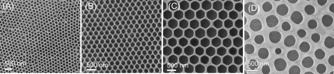 | ||
| Fig. 2 PES membranes made from (A) 150 nm, (B) 300 nm, (C) 500 nm particles, and (D) mixed 150 and 500 nm particles employing the fabrication sequence in Fig. 1A. | ||
Fig. 1B exhibits the fabrication procedure that is used to prepare 3D hemispherical nanostructures in a silicon substrate. Assembly of a particle array on a silicon substrate is followed by spin-coating of PFMPS, and by argon sputtering to open the surface of the nanoparticle array. The particles are etched away by aqueous HF before the sample is exposed to plasma etching into the underlying Si substrate and to nitric acid to remove the oxidized PFMPS. To fabricate a positive replica of the nanoparticle array into a polymer layer, the fabricated structure is used as a mold for NIL.
The initial nanoparticle array assembled from 300 nm SiO2 nanoparticles was imaged by SEM and AFM. As shown in Fig. 3(A–C), the array is highly hexagonally close-packed (hcp), with occasional domain boundaries observed, which is common for a convectively assembled nanoparticle crystal.32 The height profile of the array, as determined by atomic force microscopy (AFM), indicates that the array is uniform in curvature, as a result of the spherical nature of the particles.
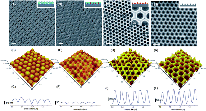 | ||
| Fig. 3 SEM and AFM images and AFM height profiles of samples made from a preformed particle array (A–C), followed by spin-coating of PFMPS and argon sputtering (D–F), HF etching (G–I) and RIE and HNO3 wet-etching (J–L). The scale bars indicate 500 nm. | ||
The spin-coating of PFMPS resulted in complete coverage of the nanoparticle array, with an excess layer of PFMPS formed on top of the array. Argon sputtering was applied to etch away the excess of PFMPS,33 exposing the top surface of the nanoparticles (Fig. 3D–F). The 3D view of the surface showed that the particles remained in hcp order and were interconnected by PFMPS. At this point, due to the infiltration of PFMPS, the roughness of the array had been diminished (Fig. 3F), however, the array still maintained some degree of curvature.
The silica nanoparticles were etched by aqueous HF, leaving a porous PFMPS layer on the surface, which resembles a negative replica of the nanoparticle array (Fig. 3G–I). High-resolution SEM (inset of Fig. 3G) revealed that the spherical porous PFMPS mask layer exhibits a bowl-like shape with the top side open. The porous PFMPS mask layer is interconnected in the array, with a height of approximately 200 nm. The height profile reveals that the PFMPS mask layer separates the pores with a PFMPS wall of at least 60 nm wide.
PFMPS, owing to the presence of ferrocene and silicon, is known to be highly resistant to reactive ion etching (RIE).27 While exposing the nanoparticle array infiltrated with PFMPS to a mixture of O2 and SF6 in RIE, the silicon underneath the PFMPS was protected from the RIE, whereas the unprotected areas were etched vertically into the silicon substrate (Fig. 1B). The substrate was subsequently sonicated in toluene and nitric acid, to remove the remaining oxidized PFMPS. A silicon substrate patterned with submicron sized and hcp ordered hexagonally shaped pores (Fig. 3J–L) was obtained without the use of lithographic techniques. The pore size was slightly enlarged to ∼300 nm and a thinner wall was observed as compared to Fig. 3G after etching into the silicon substrate which is attributed to isotropic etching of RIE. The effect of RIE was also observed in the pore shape which was changed slightly from spherical to hexagonal.
An advantage of this method is the ability to control the size of the pores and their periodicity by varying the size of the particles. In Fig. 4, examples of the patterns fabricated with particle sizes of 60, 300 and 500 nm are shown. For the particles of 500 nm (Fig. 4C), the patterns fabricated in a substrate have a spherical shape rather than hexagonal. When particles of 60 nm were used, the hole patterns were not well ordered as seen in Fig. 4A. This is attributed to the larger size distribution of the smaller particles.
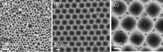 | ||
| Fig. 4 Nanosize-patterned silicon substrates prepared by using (A) 60 nm nanoparticles, (B) 300 nm particles and (C) 500 nm particles. | ||
Alternatively, the pore size can be controlled by the RIE etch time used for creating the holes in the Si substrate. Fig. 5 shows the change in the pattern shape fabricated in a silicon substrate as a function of the etching time using 300 nm particles. By increasing the etching time, the shape of patterns formed in the silicon substrate changed from spherical (Fig. 5A and 5B) to hexagonal (Fig. 5C) due to underetching of silicon underneath of PFMPS. Fig. 5D shows the relationship between the hole size and the RIE time, which indicates that the size of the pores can be easily controlled by changing the etching time. The depth of the pores after 1 min of RIE etching was ∼200 nm.
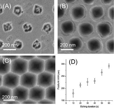 | ||
| Fig. 5 SEM images of the features obtained in silicon substrates after etching with SF6 and O2 at etching times of (A) 10 s, (B) 30 s, and (C) 60 s. Scale bars indicate 200 nm. (D) Plot of the feature size with respect to variable SF6/O2 etching duration. | ||
The patterned silicon substrates were used as molds for nanoimprint lithography (NIL). The mold was first covered with a monolayer of 1H,1H,2H,2H-perfluorodecyltriethoxysilane (PFDTS) prior to NIL. The silicon master was pressed against a silicon substrate spin-coated with poly(methyl methacrylate) (PMMA) to yield 3D hemispherical polymer features of ∼300 nm in size and 200 nm in height (Fig. 6), which is the positive replica of the original 300 nm nanoparticle array used to fabricate the mold (Fig. 1B). The 3D AFM image (Fig. 6B) shows that the patterns obtained in PMMA possess a curvature. Such patterns are hard to obtain with commercially available molds. SEM images in Fig. 6D and E show imprints in PMMA with the masters fabricated using the silica particles with 60 nm diameter, and 500 nm diameter, respectively.
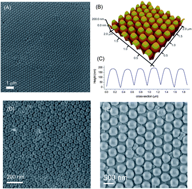 | ||
| Fig. 6 SEM (A) and AFM image (B) and height profile (C) of the PMMA nanostructure replicated from the patterned silicon masters fabricated from the 300 nm particles after 1 min of RIE with SF6/O2. SEM images of PMMA nanostructures replicated from the patterned silicon masters fabricated using 60 nm (D) and 500 nm (E) particles. | ||
It is important to control the fabrication of patterns with desired shape and height. SEM images in Fig. 7 show the imprinted structures using molds fabricated from 300 nm particles and etched with SF6/O2 plasma for 10, 30 and 60 s. respectively. Fig. 7D shows the variation in pattern height with the molds employed. Patterns with different heights and shapes were replicated depending on the mold used. The silicon substrate etched for 10 s with SF6 and O2 had a size of ∼170 nm and the replicated PMMA structures possessed nearly the same pattern size (Fig. 7A). Hexagonal patterns in PMMA were obtained by using the mold etched for 1 min (Fig. 7C). The height of the resulting PMMA patterns was ∼250 nm (Fig. 7D).
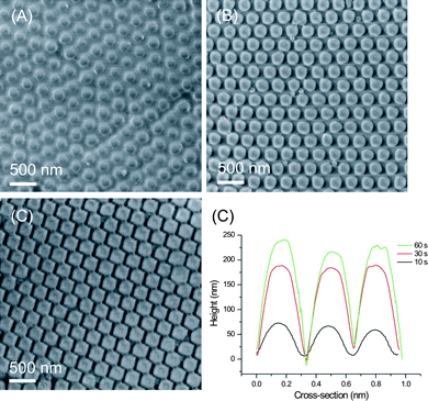 | ||
| Fig. 7 Patterns imprinted in PMMA using the molds fabricated with 300 nm silica particles etched with SF6/O2 plasma for 10 s (A), 30 s (B) and 60 s. (C). D) AFM height profiles of the imprinted PMMA structures as a function of RIE time. | ||
The Si molds made here, by nanosphere lithography using an organometallic etch mask, can be treated like Si molds made by conventional lithography techniques such as photolithography or e-beam lithography. Some molds have been used repeatedly to make nanoimprinted patterns in PMMA without any observable damage to the mold or deterioration of the imprint in the patterning step.
Conclusions
PES membranes and pores in silicon substrates with submicrometer dimension and hcp order were fabricated by nanosphere lithography. Silica nanoparticles of different sizes were used as starting materials and PFMPS as an etch-resistant polymer to produce a negative replica of the nanoparticle array. The patterned silicon substrate was later used as silicon master to replicate a positive replica of the nanoparticle array by using nanosphere lithography. By using this method, the size of the pores both in polymer and silicon substrate can be easily controlled by changing the size of the particles. It is also shown that the size and shape of the pores can be controlled by changing the etching time. Our approach opens a promising road to fabricate structures into substrates such as Si, glass as well as into polymers with low cost. Such structures can be used in the fabrication of micro-optical elements, like microlenses and microlens arrays.Acknowledgements
The Council for Chemical Sciences of The Netherlands Organization for Scientific Research (NWO-CW; Vidi Vernieuwingsimpuls grant 700.52.423 to J.H.) and the MESA+ Institute for Nanotechnology (SRO Nanofabrication) are acknowledged for financial support. We thank Mark Smithers for acquiring the SEM images.References
- C. P. Poole, and F. J. Owens, Introduction to Nanotechnology, Wiley, New Jersey, 2003 Search PubMed.
- B. D. Gates, Q. B. Xu, M. Stewart, D. Ryan, C. G. Willson and G. M. Whitesides, Chem. Rev., 2005, 105, 1171–1196 CrossRef CAS.
- Y. N. Xia and G. M. Whitesides, Annu. Rev. Mater. Sci., 1998, 28, 153–184 CrossRef CAS.
- S. Y. Chou, P. R. Krauss and P. J. Renstrom, Appl. Phys. Lett., 1995, 67, 3114–3116 CrossRef CAS.
- M. D. Austin, H. X. Ge, W. Wu, M. T. Li, Z. N. Yu, D. Wasserman, S. A. Lyon and S. Y. Chou, Appl. Phys. Lett., 2004, 84, 5299–5301 CrossRef CAS.
- P. Jiang, J. F. Bertone and V. L. Colvin, Science, 2001, 291, 453–457 CrossRef CAS.
- X. Chen, Z. M. Chen, N. Fu, G. Lu and B. Yang, Adv. Mater., 2003, 15, 1413–1417 CrossRef CAS.
- U. C. Fischer and H. P. Zingsheim, J. Vac. Sci. Technol., 1981, 19, 881–885 CrossRef CAS.
- B. T. Holland, C. F. Blanford and A. Stein, Science, 1998, 281, 538–540 CrossRef CAS.
- J. S. Yin and Z. L. Wang, Adv. Mater., 1999, 11, 469–472 CrossRef CAS.
- P. Jiang, J. Cizeron, J. F. Bertone and V. L. Colvin, J. Am. Chem. Soc., 1999, 121, 7957–7958 CrossRef CAS.
- S. B. Han, A. L. Briseno, X. Y. Shi, D. A. Mah and F. M. Zhou, J. Phys. Chem. B, 2002, 106, 6465–6472 CrossRef CAS.
- C. L. Haynes and R. P. Van Duyne, J. Phys. Chem. B, 2001, 105, 5599–5611 CrossRef CAS.
- A. A. Zakhidov, R. H. Baughman, Z. Iqbal, C. X. Cui, I. Khayrullin, S. O. Dantas, I. Marti and V. G. Ralchenko, Science, 1998, 282, 897–901 CrossRef CAS.
- A. Valsesia, P. Colpo, M. M. Silvan, T. Meziani, G. Ceccone and F. Rossi, Nano Lett., 2004, 4, 1047–1050 CrossRef CAS.
- M. Olek, J. Ostrander, S. Jurga, H. Mohwald, N. Kotov, K. Kempa and M. Giersig, Nano Lett., 2004, 4, 1889–1895 CrossRef CAS.
- J. Rybczynski, D. Banerjee, A. Kosiorek, M. Giersig and Z. F. Ren, Nano Lett., 2004, 4, 2037–2040 CrossRef CAS.
- B. Fuhrmann, H. S. Leipner, H. R. Hoche, L. Schubert, P. Werner and U. Gosele, Nano Lett., 2005, 5, 2524–2527 CrossRef CAS.
- A. Sinitskii, S. Neumeier, J. Nelles, M. Fischler and U. Simon, Nanotechnology, 2007, 18, 305307 CrossRef.
- S. H. Park and Y. N. Xia, Adv. Mater., 1998, 10, 1045–1048 CrossRef CAS.
- B. Gates, Y. D. Yin and Y. N. Xia, Chem. Mater., 1999, 11, 2827–2836 CrossRef CAS.
- S. A. Johnson, P. J. Ollivier and T. E. Mallouk, Science, 1999, 283, 963–965 CrossRef CAS.
- C. Acikgoz, X. Y. Ling, I. Y. Phang, M. A. Hempenius, D. N. Reinhoudt, J. Huskens and C. J. Vancso, Adv. Mater., 2009, 21, 2064–2067 CrossRef CAS.
- R. Rulkens, A. J. Lough and I. Manners, J. Am. Chem. Soc., 1994, 116, 797–798 CrossRef CAS.
- D. Foucher, R. Ziembinski, R. Petersen, J. Pudelski, M. Edwards, Y. Z. Ni, J. Massey, C. R. Jaeger, G. J. Vancso and I. Manners, Macromolecules, 1994, 27, 3992–3999 CrossRef CAS.
- R. G. H. Lammertink, M. A. Hempenius, J. E. van den Enk, V. Z. H. Chan, E. L. Thomas and G. J. Vancso, Adv. Mater., 2000, 12, 98–103 CrossRef CAS.
- R. G. H. Lammertink, M. A. Hempenius, V. Z. H. Chan, E. L. Thomas and G. J. Vancso, Chem. Mater., 2001, 13, 429–434 CrossRef CAS.
- X. Y. Ling, D. N. Reinhoudt and J. Huskens, Langmuir, 2006, 22, 8777–8783 CrossRef CAS.
- P. Gómez-Elipe, R. Resendes, P. M. Macdonald and I. Manners, J. Am. Chem. Soc., 1998, 120, 8348–8356 CrossRef CAS.
- X. Y. Ling, L. Malaquin, D. N. Reinhoudt, H. Wolf and J. Huskens, Langmuir, 2007, 23, 9990–9999 CrossRef CAS.
- F. Rousseaux, D. Decanini, F. Carcenac, E. Cambril, M. F. Ravet, C. Chappert, N. Bardou, B. Bartenlian and P. Veillet, J. Vac. Sci. Technol., B, 1995, 13, 2787–2791 CrossRef CAS.
- Y. N. Xia, B. Gates, Y. D. Yin and Y. Lu, Adv. Mater., 2000, 12, 693–713 CrossRef CAS.
- C. Acikgoz, M. A. Hempenius, G. J. Vancso and J. Huskens, Nanotechnology, 2009, 20, 135304 CrossRef.
Footnote |
| † These authors contributed equally to this work. |
| This journal is © The Royal Society of Chemistry 2010 |