Defect-induced junctions between single- or double-wall carbon nanotubes and metal crystals†
Julio A.
Rodríguez-Manzo
a,
Antti
Tolvanen
b,
Arkady V.
Krasheninnikov
bc,
Kai
Nordlund
b,
Arnaud
Demortière
a and
Florian
Banhart
*a
aInstitut de Physique et Chimie des Matériaux, UMR 7504 CNRS, Université de Strasbourg, France. E-mail: Banhart@ipcms.u-strasbg.fr
bMaterials Physics Division, University of Helsinki, P.O. Box 43, FI-00014, Finland
cDepartment of Applied Physics, Aalto University, P.O. Box 1100, FI-00076, Finland
First published on 23rd April 2010
Abstract
Interfaces between the ends of single- or double-wall carbon nanotubes and metal crystals (Fe, Co, Pd, and Pt) are established by electron irradiation with nanometre precision at metal–nanotube contact areas. Calculations of the bonding energies at the metal–nanotube interfaces confirm that the formation of these covalent junctions is energetically favourable in the presence of a certain concentration of structural defects in the nanotubes. The process may be endothermic or exothermic in comparison with the unconnected configuration, but in either case atomic defects in carbon nanotubes are a necessary condition for joining them with metals.
The production of nearly all structures and devices requires complex joining procedures to link together different components into a single functional structure. Since most procedures for joining macroscopic objects can hardly be applied at the nanoscale, the development of new methods for joining dissimilar nanomaterials is challenging. In the context of nanoelectronics, contacts between carbon nanotubes (CNTs) and metals are of high interest.1,2 Metals constitute the periphery for CNTs when acting as electrical contacts. Reliable mechanically stable junctions between nanotubes and metals are also crucial for the operation of electro-mechanical components. Therefore, our ability to create CNT–metal contacts as well as a thorough understanding of the interface structure and bonding are indispensable in the development of CNT-based devices.3–7
It has been demonstrated recently that junctions between multi-wall carbon nanotubes (MWNTs) and transition metals can be made by irradiating MWNTs with an electron beam in the presence of metal nanocrystals.6–9 These contacts, where the ends of MWNTs are connected to metal crystals, show covalent bonding with some metallic character, a resistance against fracture of the order of 5 GPa, and Ohmic conductance. However, the mechanisms of junction formation and the energetics of the process are still not known. The interfacial energy at a junction between a graphitic structure such as CNTs or graphene and a metal is believed to be crucial in the formation and stability of a contact,10,11 but this issue has not been studied yet.
Here we report on junctions between transition metal crystals and single- or double-wall carbon nanotubes (SWNTs, DWNTs). By carrying out experiments with a number of different metals, insight into the formation mechanism of the junctions as well as on their stability is gained. Our experimental results as well as calculations of the bonding energy show that the formation of CNT–metal contacts is favoured when the concentration of defects in CNTs exceeds a certain value at the points of contact to metal nanoparticles.
Samples containing a mixture of SWNTs and DWNTs, together with a lower percentage of MWNTs (Thomas Swan & Co. Ltd.), were dispersed in ethanol and deposited on electron microscopy copper grids. Metal nanoparticles (Fe, Co, Pd, Pt and Au) were deposited onto the nanotubes in different ways. Au and Co were deposited by magnetron sputtering at room temperature.12 Au forms isolated nanoparticles, leaving uncovered regions on the supporting CNTs.10 Co has a higher binding energy to CNTs and covers the tubes with smaller nanoparticles in a seemingly continuous way; however, a heat treatment in vacuum induced coalescence of small Co nanoparticles into larger ones. For Pd and Pt, chemically synthesized nanoparticles were deposited on the CNTs from toluene solution.13–15 For Fe nanoparticles, an unpurified sample of CVD-grown CNTs was taken where Fe has been used as a catalyst and partly remained on the tubes.16 The samples were mounted in a heating holder (Gatan) for simultaneous electron irradiation and imaging within a temperature range of 450–680 °C. The in situ experiments were carried out in a transmission electron microscope (Jeol 2100F) equipped with a Cs-corrected illumination system.
CNT–metal junctions were produced by electron irradiation of an area where a metal particle was located on top of a CNT. Electron energies of 80, 100, and 200 keV were applied, and the experiments were carried out at temperatures above 450 °C to avoid extended structural damage in the CNTs.17,18 A high spatial selectivity and current density were achieved in the scanning transmission (STEM) mode where the electron beam diameter was only 1 Å with a current density of more than 105 A cm−2 at an acceleration voltage of 200 kV. In the STEM mode, the electron beam was scanned over a pre-selected region of interest, allowing for a precise control of the irradiation.
Electron irradiation induces structural transformations by the displacement of carbon atoms in CNTs and of metal atoms on the surface of the metal crystals.17 This leads to vacancies in the CNTs as well as morphological transformations of metal particles due to surface diffusion.19–22 The formation of a metal–CNT junction depends on the energy of the electron beam, the temperature of the system, and the type of the metal. All metals of this study with the exception of Au formed junctions with CNTs. Attempts to generate junctions at electron energies of 80 keV were unsuccessful, and no links between SWNTs or DWNTs and metal crystals could be formed at this energy. Radiation effects in the tubes did not appear either. At 100 keV and above, however, structural transformations occurred, leading to the formation of metal–nanotube junctions.
Fig. 1 shows how a SWNT–metal junction is formed. In Fig. 1A the initial state of a SWNT with a Co nanoparticle on top of the tube is shown. The electron beam was converged (<5 nm) in the TEM mode, and a high electron current density (104 A cm−2) was directed onto the desired area where the SWNT touched the Co nanoparticle (arrowed in Fig. 1A). After 15 seconds of irradiation, the beam was spread and a CCD image of the resulting structure was taken (Fig. 1B). In Fig. 1A and B, irradiation was carried out at 480 °C with 100 keV electrons. Fig. 1C shows an example of a SWNT–Co–SWNT junction at 620 °C generated with 200 keV electrons. Images of three different SWNT–metal interfaces are shown in Fig. 1D–F; all were produced with a converged 200 keV electron beam at 480 °C. The lattice images show that the metal nanoparticles remain crystalline. In some cases the SWNT–metal interface was not parallel to the electron beam, thus giving the opportunity to image the cross-section of the interface (Fig. 1D) where the circular contour of the SWNT at the interface is visible. Exposure to the beam gave rise to considerable radiation damage in the CNTs close to the junction as shown in Fig. 1B. Fig. 2A–E show a process at lower beam intensity where the formation of a DWNT–Co–DWNT junction can be seen in detail over 725 seconds of irradiation. It is apparent that the reaction between the tube and the Co particle starts at the wall of contact. The Co particle moves slowly into the tube until the whole cross-section of the tube forms an interface with the metal.
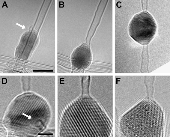 | ||
| Fig. 1 Examples of SWNT–metal contacts. (A and B) Formation of a SWNT–Co junction at 480 °C with 100 keV electrons. (C) SWNT–Co–SWNT junction formed at 620 °C with a 200 keV beam. (D–F) SWNT–metal contacts formed at 480 °C with 200 keV electrons, for Co (D and E) and Pt (F) crystals, respectively. The arrow in (D) points to the cross-section of a SWNT segment attached to a Co crystal. Scale bars: 5 nm in the top row and 2 nm in the bottom row. | ||
 | ||
| Fig. 2 (A–E) Formation of a DWNT–Co–DWNT junction. Homogenous electron irradiation (200 keV, 85 A cm−2) was applied over the complete area of view with a wide electron beam. The sample was held at 480 °C. The images were taken after 194, 335, 480, 534 and 725 seconds of irradiation, respectively. | ||
The undesired damage of the nanotubes close to the junction can be avoided by irradiating the interface area only and with high lateral selectivity. This was achieved by scanning the focused beam over the area of interest in the STEM mode of the microscope.22Fig. 3A–D show an example where a Co particle is lying on the contact point between a triple-wall carbon nanotube (TWNT) and a DWNT. The scanned area was chosen here within a rectangle of 10 nm × 3 nm, projected on a 312 × 96 pixel grid (indicated in Fig. 3A). The electron beam with 1 Å in diameter had a current density of 105 A cm−2. After each pixel of this rectangular area received a dose of 2 × 10²² electrons cm−2 (2 × 10⁶ electrons Å−2), contacts between both the TWNT and the DWNT with the Co nanoparticle were obtained (Fig. 3A–C). Care was taken to expose only the area of the CNTs adjacent to the Co nanoparticle. This is shown in Fig. 3D, where the DWNT does not show any significant damage away from the sharp DWNT–Co interface. By irradiating metal crystals on crossing CNTs, more complex structures can be formed such as multi-terminal CNT junctions9 (see Fig. S1 in the ESI†).
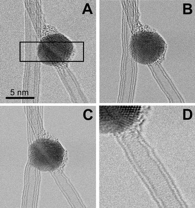 | ||
| Fig. 3 STEM irradiation of an area containing a DWNT, a TWNT, and a Co particle. The dwell time of the scanning beam was 0.4 × 10⁻⁶ seconds per pixel. After image (A) was acquired, the scanned area was reduced to the rectangular area (indicated in (A)), where the beam was scanned continuously for 614 seconds. 2 × 10⁻² seconds of irradiation were applied to each pixel. Then (B) was acquired and the same procedure was carried out for another 447 seconds until (C) was acquired. No significant damage is visible away from the junction. The wavy appearance of the vertical tubes is due to a slight vibration of the nanotubes during the time of a scan. Irradiation was carried out at 480 °C. | ||
The onset of structural transformations between 80 and 100 keV shows that a minimum energy has to be transferred to the system to induce bonding at the CNT–metal interface. The threshold electron energy for defect formation in SWNTs has been determined earlier and is 86 keV.19 Clearly higher electron energies would be required to displace metal atoms from the studied materials. For example, atom displacements in the bulk of Co would require approximately 440 keV23 and still more than 100 keV on the surface of Co crystals.24 Thus the presence of vacancies in SWNTs or DWNTs is a necessary condition for the reaction between CNTs and metal crystals. Without irradiation, the formation of junctions was not observed up to temperatures of at least 750 °C.
In order to obtain a microscopic understanding of the junction formation mechanism, we carried out atomistic computer simulations of carbon nanotube–metal particle systems within the framework of density functional theory (DFT) and by using analytical potential (AP) molecular dynamics. The details are given in the ESI†. We concentrated on the energetics of the process and, as the first approximation, neglected all effects associated with the entropy term in the free energy of the system. In our simulations, we chose iron as a metal occurring in the fcc phase in nano-sized crystals,25 as produced during the synthesis of CNTs. We also carried out DFT simulations for Co nanoparticles which gave qualitatively similar results, see Table S1 in the ESI†.
The electron beam creates defects in the nanotube, mostly vacancies as discussed above. This is associated with an increase in the potential energy of the system as shown in Fig. 4. As divacancies have low formation energy26 and easily appear under electron irradiation due to coalescence of single vacancies, one can assume that the energy increase associated with isolated defects is simply the number of divacancies times the divacancy formation energy (about 5 eV26). To assess the energetics of the junction formation process, one can assume that all vacancies form a big cluster just under the particle. As evident from Fig. 4, it is energetically favourable to have a “big hole” in a (10,0) nanotube rather than isolated divacancies. Moreover, if the number of displaced atoms is more than 14, it costs less energy to cut the tube into two halves (red horizontal dashed line in the figure) than to generate a big vacancy cluster, as the number of dangling bonds would be smaller in the cut tube.
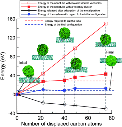 | ||
| Fig. 4 Energetics of the system during the formation of metal–nanotube junctions under electron irradiation. The upper curve (open squares) gives an estimate of the energy required to create a certain number of isolated divacancies in a (10,0) nanotube. The curve with full squares stands for energies of the nanotube with the same number of displaced atoms forming a big vacancy cluster under the particle as calculated using the AP approach. The curve with open circles corresponds to energy released due to adsorption of the metal particle on the vacancy cluster. The net value (the difference between the energy required to cut the tube and the released energy due to the interaction with the metal cluster) corresponds to the curve with full circles. The total number of C atoms is always the same: the displaced atoms are added at the ends of the nanotube. | ||
The interaction of the metal particle with the defected tube lowers the energy of the system. The dependence of the energy released due to adsorption of the particle on the vacancy cluster is also shown by the black curve with open circles in Fig. 4. The net value (blue curve) for intermediate configurations is positive, meaning that the energy is higher than that for the intact structure. Ultimately, it should converge to the energy corresponding to the fully cut tubes with its halves being attached to the particle. In the simulations the energy can be higher, as the particular configurations not necessarily represent the minimum energy configuration for the given number of displaced atoms.
To get further insight into the driving force for the system evolution, one can concentrate on the energy difference between the initial configuration, an imaginary configuration when the tube is cut into two halves, and the final configuration with the covalent bonds between the halves of the tube and the metal particles (Fig. 5). Our DFT (resp. AP) simulations showed that it costs about EbondC–C ≈ 6 (resp. 4) eV per bond to break a tube, with the value of EbondC–C depending on the tube chirality and diameter. Then the gain in energy due to new carbon–metal bonds between the particle and the halves of the nanotubes can be evaluated. The DFT and AP results proved to depend heavily on the size of the cluster and its orientation with regard to the nanotube (see ESI†). We found that about 20 eV can be released when a (7,0) tube is attached to the metal particle (the value of about 40 eV we got for a small Fe55 particle is anomalously high due to the very small size of the particle), and twice as much when two halves of the tube form a junction. Qualitatively similar results were obtained for a (8,0) nanotube connected to the Fe slab, Fig. 5(d). The energy release due to new bonds can be evaluated, normalized to the number of cut bonds, and compared to the energy of a broken C–C bond. We stress, however, that per each broken C–C bond, two C–metal atom bonds are formed. Our DFT results indicate that the energy of the final configuration representing a particle attached to the ends of the two SWNTs is close to the energy of the isolated perfect nanotube (without vacancies) and the metal particle. In any case the junction is more stable than the isolated metal particle plus two halves of the cut nanotube. At the same time, the electron beam is necessary to produce defects and thus increases the average potential energy per C atom in the irradiated area so that the system can go over the potential barriers separating different configurations.
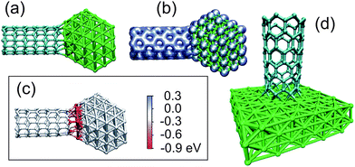 | ||
| Fig. 5 Molecular models of SWNTs attached to Fe particles. The atomic structure (a) and the electron density (b) of a (7,0) SWNT–Fe116 particle junction as revealed by DFT calculations. (c) The same system calculated by the analytical potential method. The atoms are coloured according to the difference in potential energy of the atoms in the junction configuration compared to the isolated nanotube plus metal particle; that is EC–M − Edb is visualized for C atoms, and EM–C − Esurf for Fe atoms. Red colour represents a drop in energy, blue an increase. It is evident that the energy for most of the atoms in the junctions decreases. (d) (8,0) SWNT on a Fe surface mimicking the structure of the junction between nanotubes and big metal particles as calculated by the DFT approach. | ||
The important quantity is the relation between the loss and gain in energy ΔE between the initial and final configurations per broken bond in the nanotube:
| ΔE = EbondC–C − 2EbondC–M, | (1) |
Fig. 5(c) presents a molecular model of a (7,0) nanotube attached to a Fe116 particle. The atoms are coloured according to the difference in the potential energy of the atoms in the junction configuration and for the isolated metal particle and nanotube with the open end. Red colour corresponds to a drop in energy, blue to an increase. It is evident from Fig. 5(c) that the potential energy decreases for most of the atoms in the junction area, resulting in the overall drop in energy by about 9.5 eV (19 eV for two junctions).
Assuming that the number of broken bonds which appeared when the tube was cut by the beam is approximately half of the number Ndb of atoms with dangling bonds (for the two halves of the nanotube), and neglecting the difference in the energy of the inner atoms, the difference in total energy between the initial and final configurations can be written as
| ΔEtot = Ndb(EC–M − Esp2) + Nsurf(EM–C − Esurf), | (2) |
| ΔE = Ebondcut − Ebondrel = 2(EC–M − Edb + EM–C − Esurf) + Ebondcut. | (3) |
To conclude, we have demonstrated that junctions between the ends of single- or double-wall carbon nanotubes and several types of metals (Fe, Co, Pd, and Pt) can be made when the nanotubes contain a certain number of lattice defects. Electron irradiation is just one possibility of inducing these defects, although this technique is able to generate defects in a pre-defined area with sub-nanometre resolution. Other techniques might be applicable on a larger scale, e.g., ion irradiation or a chemical or plasma treatment of CNTs that may produce a large number of dangling bonds. In view of the importance of metal–CNT contacts, the understanding of the prerequisites for the formation of junctions, i.e., the presence of defects in the CNTs, is mandatory for the development of CNT-based devices.
Acknowledgements
Support from the Deutsche Forschungsgemeinschaft (BA 1884/6-1) and the Région Alsace (480-09) is gratefully acknowledged. This work was also supported by The Academy of Finland through several projects. We thank the Finnish IT Center for Science for generous grants of computer time, and M. Acosta for assistance with the magnetron sputtering.References
- W. Lu and C. M. Lieber, Nat. Mater., 2007, 6, 841–850 CrossRef CAS
.
- C. Jin, K. Suenaga and S. Iijima, Nat. Nanotechnol., 2008, 3, 17–21 CrossRef CAS
- J. Hu, M. Ouyang, P. Yang and C. Lieber, Nature, 1999, 399, 48–51 CrossRef CAS
- Y. Zhang, T. Ichihashi, E. Landree, F. Nihey and S. Iijima, Science, 1999, 285, 1719–1722 CrossRef CAS
- K. Asaka, H. Nakahara and Y. Saito, Appl. Phys. Lett., 2008, 92, 023114 CrossRef
- J. A. Rodríguez-Manzo, F. Banhart, M. Terrones, H. Terrones, N. Grobert, P. M. Ajayan, B. G. Sumptere, V. Meuniere, M. Wang, Y. Bando and D. Golberg, Proc. Natl. Acad. Sci. U. S. A., 2009, 106, 4591–4595 CrossRef CAS
- F. Banhart, Nanoscale, 2009, 1, 201–213 RSC
- M. Wang, Y. Bando, J. A. Rodrígez-Manzo, F. Banhart and D. Golberg, ACS Nano, 2009, 3, 2632–2638 CrossRef CAS
- J. A. Rodríguez-Manzo, M. Wang, F. Banhart, Y. Bando and D. Golberg, Adv. Mater., 2009, 21, 4477–4482 CrossRef CAS
- Y. Zhang, N. W. Franklin, R. J. Chen and H. Dai, Chem. Phys. Lett., 2000, 331, 35–41 CrossRef CAS
- A. Börjesson, W. Zhu, H. Amara, C. Bichara and K. Bolton, Nano Lett., 2009, 9, 1117–1120 CrossRef
- Y. Zhang and H. Dai, Appl. Phys. Lett., 2000, 77, 3015–3017 CrossRef CAS
- A. Demortière and C. Petit, Langmuir, 2007, 23, 8575–8584 CrossRef CAS
- A. Demortière, P. Launois, N. Goubet, P.-A. Albouy and C. Petit, J. Phys. Chem. B, 2008, 112, 14583–14592 CrossRef CAS
- K. Naoe, C. Petit and M. P. Pileni, Langmuir, 2008, 24, 2792–2798 CrossRef CAS
- F. Lupo, J. A. Rodríguez-Manzo, A. Zamudio, A. L. Elías, Y. A. Kim, T. Hayashi, M. Muramatsu, R. Kamalakaran, H. Terrones, M. Endo, M. Rühle and M. Terrones, Chem. Phys. Lett., 2005, 410, 384–390 CrossRef CAS
- F. Banhart, Rep. Prog. Phys., 1999, 62, 1181–1221 CrossRef CAS
- A. V. Krasheninnikov and F. Banhart, Nat. Mater., 2007, 6, 723–733 CrossRef CAS
- B. W. Smith and D. E. Luzzi, J. Appl. Phys., 2001, 90, 3509–3515 CrossRef CAS
- J. Li and F. Banhart, Nano Lett., 2004, 4, 1143–1146 CrossRef CAS
- M. D. Fischbein and M. Drndić, Nano Lett., 2007, 7, 1329–1337 CrossRef CAS
- A. Zobelli, A. Gloter, C. Ewels and C. Colliex, Phys. Rev. B: Condens. Matter Mater. Phys., 2008, 77, 045410 CrossRef
-
P. Ehrhart, P. Jung and H. Schultz, in Atomic Defects in Metals, ed. H. Ullmaier, Landolt-Börnstein, New Series, Group 3, Springer-Verlag, Berlin, 1991 Search PubMed
- R. F. Egerton, P. Li and M. Malac, Micron, 2004, 35, 399–409 CrossRef CAS
- B. Wei, M. Shima, R. Pati, S. K. Nayak, D. J. Singh, R. Ma, Y. Li, Y. Bando, S. Nasu and P. M. Ajayan, Small, 2006, 2, 804–809 CrossRef CAS
- A. V. Krasheninnikov, P. O. Lehtinen, A. S. Foster and R. M. Nieminen, Chem. Phys. Lett., 2006, 418, 132–136 CrossRef CAS
- O. V. Yazyev and A. Pasquarello, Phys. Rev. Lett., 2008, 100, 156102 CrossRef
- A. V. Krasheninnikov, P. O. Lehtinen, A. S. Foster, P. Pyykkö and R. M. Nieminen, Phys. Rev. Lett., 2009, 102, 126807 CrossRef CAS
Footnote |
| † Electronic supplementary information (ESI) available: A description of the tailoring of CNT–metal junctions by the electron beam and details of the calculations. See DOI: 10.1039/c0nr00098a |
| This journal is © The Royal Society of Chemistry 2010 |