Tailoring morphology in free-standing anodic aluminium oxide: Control of barrier layer opening down to the sub-10 nm diameter†
Jie
Gong‡
a,
William H.
Butler
a and
Giovanni
Zangari
*b
aCenter for Materials for Information Technology, University of Alabama, Tuscaloosa, AL 35487-0209
bDepartment of Materials Science and Engineering and CESE, University of Virginia, 395 McCormick Rd., P.O. Box 400745, Charlottesville, VA 22904-4745, USA. E-mail: gz3e@virginia.edu; Tel: +1-434-243-5474
First published on 18th March 2010
Abstract
Free-standing, highly ordered porous aluminium oxide templates were fabricated by three-step anodization in oxalic, sulfuric or phosphoric acid solutions, followed by dissolution of the aluminium substrate in HgCl2. Opening of the pore bottoms on the barrier layer side of these templates was carried out by using chemical or ion beam etching. Chemical etching is capable of achieving full pore opening, but partial pore opening occurs inhomogeneously. On the contrary, ion beam etching enables homogeneous and reproducible partial pore opening, with the pore size controlled through the etching time. By this method, pore openings as small as 5 nm can reliably be obtained.
1. Introduction
Nanoporous anodic aluminium oxide (AAO) is finding wide application as a template for the fabrication of one-dimensional nanostructures1 or two-dimensional patterns,2–6 as a photonic crystal,7 in nanofluidics8 and filtration,9 in magnetic information storage,10 sensing,11 and even in biomedical applications such as drug delivery.12 AAO is formed by the electrochemical oxidation of aluminium (Al) in an appropriate acidic electrolyte, and consists of an array of parallel nanochannels perpendicular to the original Al surface, closed at the bottom by a hemispherical oxide film known as the barrier layer.13–15AAO has been known for more than 50 years,16 but only after 1995, when Masuda and Fukuda reported the synthesis of a highly ordered pore array by two-step anodization in oxalic acid,2 its potential in nanofabrication was appreciated and related research efforts flourished. The self-organized pore growth process, leading to a densely packed hexagonal pore structure, is controlled through the electrolyte chemistry, applied voltage, and processing time. Self-organized growth has been achieved in oxalic,2,17–19 sulfuric,17–20 and phosphoric acids,18,19,21,22 and mixed oxalic and sulfuric acid solutions.23 Interpore distance and pore diameter can be varied between 50–500 nm and 5–300 nm, respectively, depending on the electrolyte and anodization voltage employed;18,24 in addition, the latter can be widened by chemical etching in diluted acids. Long range ordering of the porous structure can be achieved using a two or three-step anodization process2,25 or by pre-texturing the initial aluminium surface via nanoimprint,26,27 nanoindentation,28 or ion beam prepatterning.29
Many applications of AAO in nanofabrication require opening of the pore bottom; this has been achieved by chemical etching in acidic solutions,30 ion beam31 or plasma etching.3 Complete removal of the pore bottom results in an opening with the same size as the channel; however, in some cases, close control over the diameter of the opening, below the channel diameter, may be required. This is particularly important, for example, in the fabrication of nanoconstrictions for magnetic point contacts32 or for the control of magnetic domain wall motion33 in spintronic applications, as well as in the synthesis of molecular membranes.34,35
Partial pore opening of oxalic acid anodized AAO by wet chemical etching has been recently reported;30 however, no detailed comparison of this process with ion beam etching has been carried out. Furthermore, although ion beam etching methods have demonstrated the uniform engraving of holes on the hemispherical shaped surface of the barrier layer with diameter as small as 10 nm using oxalic acid AAO,31 no such process has been reported for phosphoric or sulfuric acid AAO, which could produce larger or smaller nanoholes, respectively, due to the different size of the porous structures. In this work, free-standing sulfuric, oxalic and phosphoric acid AAO have been synthesized by a three-step anodization process, and the effects of chemical and ion beam etching on the morphology of sulfuric, oxalic and phosphoric acid AAOs with different pore sizes have been compared. It is demonstrated that uniformly engraved holes with diameter down to 5 nm can be reliably obtained using ion beam etching of sulfuric acid AAO. Fig. 1 depicts a schematic diagram of the barrier opening processes discussed in this paper, and provides a qualitative illustration of the resulting AAO nanostructures.
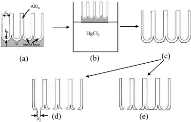 | ||
| Fig. 1 Schematic view of the fabrication process of free-standing porous AAO with the barrier layer perforated by wet chemical or ion beam etching. (a) AAO after anodization; (b) chemical post treatment to remove the metallic Al support; (c) free-standing AAO before etching; (d) uniform controllable openings on the barrier side achieved by ion beam etching; and (e) non-uniform openings on the barrier side obtained by wet chemical etching. d1: constriction/opening size; tb: barrier layer thickness; dp: pore diameter. | ||
2. Experimental
Chemicals
All chemicals used in this work were of analytical grade. All solutions were prepared, and rinsing as well as cleaning were performed, using Milli-Q water (resistivity 18.2 MΩ cm).Aluminium sheet pretreatment
A high purity polycrystalline aluminium (Al) sheet sample (99.998%, Alfa Aesar) was first degreased in a 5% NaOH solution at 60 °C for 30 s, rinsed, and then neutralized in 1![[thin space (1/6-em)]](https://www.rsc.org/images/entities/char_2009.gif) :1 HNO3 for 5–10 s. After thorough rinsing in water, the substrate was electropolished (Buehler Electropolisher-4, 32 V, 45–60 s) in perchloric acid–ethanol electrolyte (165 mL 65% HClO4, 700 mL ethanol, 100 mL 2-butoxyethanol “butylcellusove”, and 137 mL H2O). The sheet was then washed, first in warm and then in cold water. Atomic Force Microscopy AFM was utilized to characterize the topography and roughness of the polished surface.
:1 HNO3 for 5–10 s. After thorough rinsing in water, the substrate was electropolished (Buehler Electropolisher-4, 32 V, 45–60 s) in perchloric acid–ethanol electrolyte (165 mL 65% HClO4, 700 mL ethanol, 100 mL 2-butoxyethanol “butylcellusove”, and 137 mL H2O). The sheet was then washed, first in warm and then in cold water. Atomic Force Microscopy AFM was utilized to characterize the topography and roughness of the polished surface.
Aluminium anodization
The pretreated Al sheet, with a polished active area of 3 cm2, was used as the anode during anodization. A degreased and neutralized 98.5% pure Al sheet with an area ten times larger (36 cm2) than the anode was used as the cathode. Anodization was performed under potentiostatic control, and the current transient during anodization was recorded by monitoring the voltage drop across a standard resistor (R = 10 Ohm) connected in series. The temperature of the electrolyte was maintained at specific values using a jacketed beaker and a cooling system (Fisher Scientific, Model ISOTEMP 1016D Circulator). The solution was stirred vigorously using a magnetic stirrer in order to accelerate dispersion of the heat generated by the sample during anodization. Anodization was performed in one of three electrolyte systems, i.e. sulfuric (0.3 M, 3 °C), oxalic (0.3 M, 15 °C) or phosphoric acid (1 M, 3 °C), to produce AAO films with different geometries (different interpore distances and pore diameters).Highly ordered AAO templates were prepared using a multi-step anodization process according to the following scheme:25
1. A polished Al sheet was anodized for 5–15 min to morphologically “texture” the Al surface.36
2. The resulting oxide film was dissolved in a solution containing 0.2 M H2CrO4 and 0.4 M H3PO4 at 60–70 °C for 5–20 min.
3. The substrate was re-anodized for more than 12 h to create long-range ordering.
4. Step 2 was repeated, with a duration of more than 30 min to dissolve the thick oxide film formed in step 3.
5. The substrate was finally anodized for a varying period of time, depending on the thickness of the AAO film desired.
Post-treatment and template fabrication
To completely dissolve the metallic Al substrate without etching the AAO membrane, the highly ordered, supported AAO film was carefully floated on the Al side on a saturated mercuric chloride (HgCl2) solution for 4–6 h (Fig. 1). Caution! HgCl2 is harmful if swallowed, inhaled or absorbed through skin. It should be handled with extreme care using goggles, lab coat and proper gloves. The AAO film was gently rinsed and dried in vacuum over a desiccator (P2O5). The barrier layer was then controllably removed by chemical etching (CE) in 5% H3PO4 solution at room temperature (25 °C) or by ion beam etching (IBE).A Veeco Microetch RF-1201 Ion Beam Etching System was employed for IBE. An inductively-coupled RF ion source was used, together with a Plasma Bridge Neutralizer (PBN) to keep the ion beam collimated. The ion beam etching chamber was first pumped down to 7–8 × 10⁻⁷ torr, then Ar gas flowed into the chamber at 20 sccm (standard cubic centimetre per minutes), keeping the chamber pressure constant at 1.32–1.34 × 10⁻⁴ torr. During etching, a 450 V beam voltage and 450 mA beam current were employed. Suppressor voltage was 300 V, and incident RF power was 300 W. PBN Ar gas flow rate was 3 sccm, and the ratio of neutralizer current/beam current (K factor) was 1.1. The ion beam incidence angle was 45°; the sample fixture was rotated at 0.1 revolutions per second and water cooled. The etching rate, calibrated using a Si wafer, was 40 nm min−1. When converted to Al2O3 using a standard milling rate table, the etching rate was about 9 nm min−1.
Characterization
Scanning electron microscopy (SEM, Philips model XL 30) and atomic force microscopy (AFM, Digital Instruments, Dimension 3000) were employed to characterize the surface morphology and topography, respectively. The analyses using AFM were performed in tapping mode in air and the scan rate was kept at 1 Hz or lower. Mikromasch ultrasharp silicon cantilevers, with radius of curvature <10 nm, tip height of 15–20 μm, full tip cone angle <20°, were used for AFM characterization. The regularity of the hexagonally patterned nanohole arrays was assessed quantitatively by fast Fourier transformation (FFT) of the AFM images, using the proprietary software (Nanoscope V) available with the AFM. The barrier side constriction size distribution after ion beam etching was evaluated by direct measurement of more than 50 openings in three AFM images taken at different locations.3. Results and discussion
3.1. Anodization process and sample characterization
The purpose of the surface pretreatment is to clean and eliminate the main surface defects, while minimizing internal stresses present at the surface. The AFM surface topography after pretreatment is shown in Fig. S1 of the ESI.† The surface appears smoother and glossier than before electropolishing. The root-mean-square (RMS) roughness as determined by AFM is 1.2 nm over a 4 × 4 μm2 area.Anodization was carried out under potentiostatic conditions in H2SO4, oxalic acid ((COOH)2) or H3PO4 solutions. Voltages were chosen in the range of values yielding long range order.18 Typical current density–time (I–t) curves in H2SO4 for the first and second anodization are shown in Fig. 2; the same plots for oxalic and phosphoric acid solutions are reported in Fig. S2 of the ESI.† All curves show four stages of pore formation (Fig. 2, 1st anodization). In stage I, current drops abruptly due to the formation of the planar barrier oxide layer. In stage II, current gradually increases and after different time intervals (dependent on the solution and voltage applied) reaches its maximum between stages II and III. The increase in current is characteristic for porous AAO formation, indicating that field-enhanced dissolution starts to concentrate at locally convex surface regions, nucleating the pores.25 In stage III, the current decreases slightly to a constant value, indicating that the first initiated disordered pores are becoming hexagonally ordered, and stationary pore growth has been attained (stage IV).25
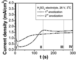 | ||
| Fig. 2 Typical anodization curves (current density vs. time, I–t) for two-step aluminium anodization in a sulfuric acid electrolyte (0.3 M H2SO4, 26 V, 3 °C). | ||
Comparison of the 1st anodization on the electropolished flat surface and the 2nd anodization on the “textured” surface in the three electrolyte systems shows that the pore nucleation process (stage II) is greatly shortened on the “textured” surface. In addition, the lowest current on the flat surface is always much lower than on the “textured” surface. This implies that “pre-texturing” the surface accelerates the ordered pore initiation process. For both the 1st and 2nd anodization, the duration of regime II follows the trend H3PO4 (185 V) > (COOH)2 (40 V) > H2SO4 (26 V), which corresponds to the difficulty of achieving ordering and the barrier layer thickness.
The fabrication process and porous structure of AAO were studied in detail in H2SO4, (COOH)2 and H3PO4 solutions. The process parameters and extracted geometrical characteristics are summarized in Table 1. Fig. 3(a) and (b) compare the topography, as determined by AFM, of the AAO surface after the 2nd and 3rd anodization in oxalic acid, respectively. Fast Fourier transform (FFT) patterns of the images, giving information about the structural periodicity in the inverse (momentum) space are shown in the corresponding insets. Both the AFM topography and the FFT patterns show that the number of defects decreases and the pore ordering improves after the 3rd anodization step. The diffraction ring and its broadening observed in the FFT of Fig. 3(a) indicate that 2D ordering of the structure is imperfect and that the interpore distance varies across the area of the sample. The barrier side topographic image (Fig. 3(c)), obtained by separation of the AAO membrane after the 3rd anodization step in saturated HgCl2, shows highly ordered, hexagonal patterns of hemispherical domes. The FFT images of the front and barrier side of AAO surfaces anodized three times consist of six equidistant and distinct spots, indicative of a perfectly ordered hexagonal pore lattice. Additional characterization and images of the AAO obtained in oxalic, sulfuric and phosphoric acid are available in the ESI.†
| Process steps | H2SO4 (26 V, 3 °C) | (COOH)2 (40 V, 15 °C) | H3PO4 (185 V, 3 °C) |
|---|---|---|---|
| 1st anod. time/min | 5 | 5 | 15–20 |
| 1st oxide strip time/min | 10–15 | 10–15 | >30 |
| 2nd anod. time/h | >12 | >12 | 16–20 |
| 2nd oxide strip time/min | 30–45 | 30–45 | 120 |
| Growth rate/μm h−1 | 3.5 | 6 | 7.5 |
| Interpore distance/nm | 60 | 108 | 450 ± 50 |
| Pore density/cm−2 | ∼3 × 10¹⁰ | ∼1 × 10¹⁰ | ∼5 × 10⁸ |
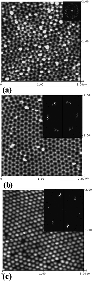 | ||
| Fig. 3 AFM surface topography of oxalic acid anodized AAO and the fast Fourier transform (FFT) patterns: (a) after 2nd anodization; (b) after 3rd anodization; (c) highly ordered hemispherical domes on the barrier side after dissolution of non-anodized aluminium. | ||
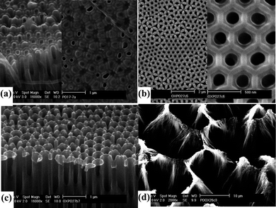
Similar to anodization on pre-textured Al substrates either by lithography22 or by nanoimprinting/nanoindentation,26–28 a pore array pattern with double periodicity can, in principle, be obtained by first anodizing in oxalic acid, then in sulfuric acid. The resulting morphology of the pore opening and barrier layer are shown in Fig. 4. Obviously, the pore-to-pore distance in the AAO obtained by anodization at a different voltage (25–27 V) in sulfuric acid does not match the pitch of the pattern obtained in oxalic acid at 40 V. Therefore, the pores growing in the second stage will not follow the pre-patterned pits and a distorted pore arrangement will occur. The anodic pores produced in H2SO4 have a much higher density than the pre-existing pits, and are mostly located along the pattern ridges, with each pattern cell containing nearly the same number of pores. It is also interesting to note that, if the anodization sequence is reversed, i.e. anodizing in sulfuric acid followed by oxalic acid, the final pattern shows the same features as after anodization in oxalic acid alone.
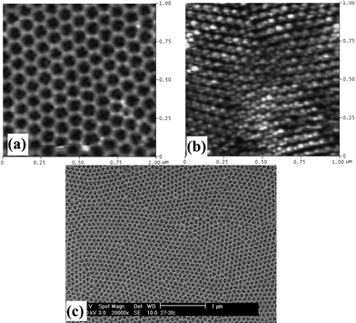 | ||
| Fig. 4 Double periodicity obtained by anodizing in oxalic acid (1st and 2nd step), followed by anodization in sulfuric acid (3rd step): (a) front side and (b) barrier side AFM surface topography, (c) SEM large area morphology. | ||
3.2. Barrier layer etching processes
The barrier layers present at the bottom of the pores of the AAO channels were opened by using one of two methods: wet chemical etching or ion beam etching.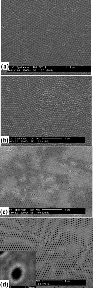 | ||
| Fig. 5 SEM surface morphology of the barrier side of oxalic acid-anodized AAO after different etching times in 5% H3PO4 at room temperature (25 °C): (a) 25 min; (b) 30 min; (c) 35 min; and (d) 40 min. The inset in (d) shows an enlarged view of the pore opening. | ||
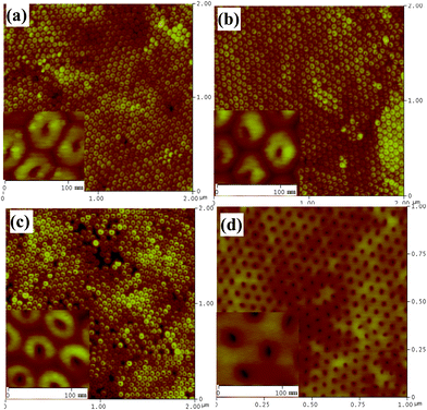
As a comparison, the results of CE after various etching times for H2SO4-anodized AAO (Fig. 6) and H3PO4-anodized AAO (Fig. 7) are also shown. As expected, due to the different barrier layer thickness in the three cases, the times necessary to fully open the barrier caps are quite different. For H2SO4-anodized AAO, 20–25 min of etching is sufficient (Fig. 6(d)); H3PO4-anodized AAO on the other hand needs 240 min to fully open the pores (Fig. 7(b)). Again, CE can conveniently open the barrier layer to a full extent, but it does not allow accurate control of the size and location of the openings. As shown by AFM topography in Fig. 6(a1–d1), CE generates a rough and irregular barrier side, resulting in inhomogeneous etching, and thus hindering prospective integration with other components. It is also interesting to note that, if the H3PO4-anodized AAO is over-etched, the walls of the AAO channels are etched at a much slower rate than the backbone, probably due to preferential anion incorporation at walls,15 or to differences in chemical composition27,30 or crystallinity15 between the inner and outer region. As a result, alumina fibers can be produced, as also reported in ref. 37.
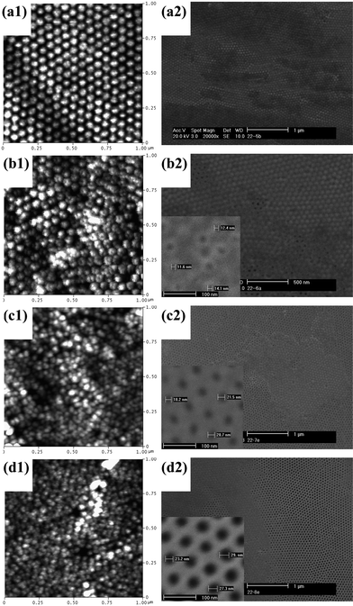 | ||
| Fig. 6 AFM (a1–d1) and SEM (a2–d2) images of the barrier side of sulfuric acid-anodized AAO membranes after different etching times in 5% H3PO4 at room temperature (25 °C): (a) 5 min; (b) 10 min; (c) 15 min; and (d) 20 min. The insets in (b2), (c2) and (d2) show enlarged views of the corresponding images. | ||
 | ||
| Fig. 7 SEM micrographs of the barrier side of phosphoric acid-anodized AAO membranes after different etching times in 5% H3PO4 at room temperature (25 °C): (a) 220 min (left: tilted angle view; right: planar view; same scale bar); (b) 240 min (left and right image scans are at different magnifications); (c) 260 min; and (d) 285 min. | ||
Inhomogeneous pore etching by CE may be explained in terms of faster etching at defect sites (grain boundaries of the initial Al surface or boundaries of the ordered pore domains) or at regions with a thinner barrier layer. An initial, small difference in etching rate at separate locations may cause a local depletion of the etchant and preferential diffusion of the etchant from the bulk solutions to these regions, resulting in positive feedback. This effect may explain the clustering of opened pores observed in Fig. 6 (b2) (probably a domain boundary), or Fig. 6 (c2) (probably a region with locally thinner barrier layer).
The AFM topography of oxalic acid-anodized AAO barrier side after different IBE processing times is shown in Fig. 8. Uniform and round holes (diameter 15–30 nm) can be obtained over a large area when the etching time is limited to 5–10 min (Fig. 8(b) and (c)). Round hemispherical caps are uniformly milled from the top due to the uniform flux distribution of the ion beam. Chemical composition15 or stress38 gradients that may be present in the barrier layer at the pore bottom are of no consequence, since the energy differences involved due to these gradients are much smaller than the ion beam energy. Long-time etching leads to the disappearance of the protruding caps and results in holes with shape and diameter similar to the nanopores on the opposite side (Fig. 8(d)). This indicates that the hemispherical barrier layer domes are completely etched away by the ion beam.
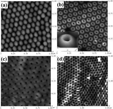 | ||
| Fig. 8 AFM surface topography of the barrier side of oxalic acid-anodized AAO membranes after different ion beam etching times. (a) no etching; (b) 5 min (inset shows the enlarged 3D AFM image of a single cap); (c) 10 min; and (d) 15 min. | ||
Much smaller constrictions can be obtained by IBE from the barrier layer side of H2SO4-anodized AAO in shorter times. This is due to the fact that the pore size and the barrier thickness of these AAO samples are smaller. The morphologies resulting from the etching process are shown in Fig. 9 and 10. As shown in Fig. 9, very uniform small openings over a large area can be engraved on the barrier side. The opening size can be accurately controlled down to about 5–8 nm by limiting the etching time to 2–4 min. Increasing etching time results in increased opening size up to more than 18 nm, as well as a flattened surface topography (Fig. 10).
 | ||
| Fig. 9 AFM surface topography of the barrier side of sulfuric acid-anodized AAO after different ion beam etching times: (a) 2 min; (b) 4 min; (c) 8 min; and (d) 12 min. Insets in (a)–(d) show corresponding enlarged AFM images. | ||
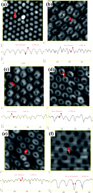 | ||
| Fig. 10 AFM surface topography (top) and profiles (bottom) of the barrier side of sulfuric acid-anodized AAO membranes after different ion beam etching times: (a) no etching, top height 8.3 nm; (b) 2 min, 3.9 nm; (c) 4 min, 3.1 nm; (d) 8 min, 2.7 nm; (e) 10 min, 2.1 nm; and (d) 12 min, 0 nm, the surface is completely flattened by ion beam etching. | ||
IBE of H3PO4-anodized AAO produces larger openings, ranging from 100 to 200 nm, as shown in Fig. 11. The etching time necessary to open the hemispherical domes is much longer now since the barrier layer is thicker in these samples. Although every dome in the images can be opened, the shape and size of the openings are not uniform on the same sample. This is probably a consequence of the fact that pores and barrier domes on phosphoric acid-anodized AAO are not as ordered as those obtained using the other acids. As shown in Fig. 11(c) and (d), triangular, trapezoidal, square and round openings can be found.
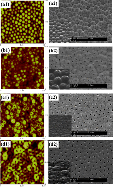 | ||
| Fig. 11 AFM (a1–d1) and SEM (a2–d2) images of the barrier side of phosphoric acid-anodized AAO membranes after different ion beam etching times: (a) no etching; (b) 50 min; (c) 80 min; and (d) 100 min. Insets in (a2)–(d2) show tilted angle SEM views (same scale bar). | ||
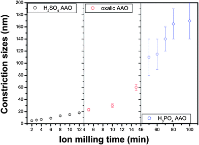
The constriction size, defined as the full width at half depth of the AFM topographic scans across the barrier side openings, produced by ion beam etching on the three types of AAOs are extracted and summarized in Fig. 12. A broad range of constriction sizes can be obtained; in addition, the size distribution is narrow, with the exception of the H3PO4-anodized AAO. IBE processing of AAO, therefore, provides ideal templates to grow nanoconstrictions with closely controlled geometry, or to fabricate molecular membranes with closely controlled pore size in the deep sub-μm range.
4. Conclusions
Free-standing sulfuric, oxalic and phosphoric acid-anodized AAO membranes, with pore diameter ranging from 20 to 400 nm, have been synthesized by a three-step anodization process and successive Al stripping. Chemical and ion beam etching were employed to open the pore bottoms of these AAO samples and their morphological characteristics were compared. Chemical etching conveniently enables full opening of the channel array templates, however, locations of the opened regions and their size are difficult to control, particularly when partial pore opening is sought. These inhomogeneities appear to be a consequence of pre-existing non-uniformities and/or defects in the AAO barrier layer. Ion beam etching, on the other hand, is capable to engrave uniform holes on the barrier side, with pore size controllable by the etching time. Uniformly engraved holes, with diameter down to 5 nm, can be obtained using sulfuric acid-anodized AAO and ion beam etching; this process has potential applications in the nanofabrication of constrictions with controlled size, down to the deep sub-μm range.Acknowledgements
The support of NSF through grant NSF MRSEC DMR 0213985 is gratefully acknowledged.References
- Y. Lei, W. P. Cai and G. Wilde, Highly ordered nanostructures with tunable size, shape and properties: A new way to surface nano-patterning using ultra-thin alumina masks, Prog. Mater. Sci., 2007, 52(4), 465–539 CrossRef CAS.
- H. Masuda and K. Fukuda, Ordered Metal Nanohole Arrays Made by a 2-Step Replication of Honeycomb Structures of Anodic Alumina, Science, 1995, 268(5216), 1466–1468 CrossRef CAS.
- J. Liang, H. Chik, A. Yin and J. Xu, Two-dimensional lateral superlattices of nanostructures: Nonlithographic formation by anodic membrane template, J. Appl. Phys., 2002, 91, 2544–2546 CrossRef CAS.
- M. Sun, G. Zangari, M. Shamsuzzoha and R. M. Metzger, Electrodeposition of highly uniform magnetic nanoparticle arrays in ordered alumite, Appl. Phys. Lett., 2001, 78, 2964–2966 CrossRef CAS.
- K. Nielsch, F. Müller, A.-P. Li and U. Gösele, Uniform Nickel deposition into ordered alumina pores by pulsed electrodeposition, Adv. Mater., 2000, 12, 582–586 CrossRef CAS.
- B. Cheng and E. T. Samulski, Fabrication and characterization of nanotubular semiconductor oxides In2O3 and Ga2O3, J. Mater. Chem., 2001, 11, 2901–2902 RSC.
- I. Mikulskas, S. Juodkazis, R. Tomasiunas and J. G. Dumas, Aluminium oxide photonic crystals grown by a new hybrid method, Adv. Mater., 2001, 13(20), 1574–1577 CrossRef CAS.
- L. G. A. van de Water and T. Maschmeyer, Mesoporous membranes - a brief overview of recent developments, Top. Catal., 2004, 29(1–2), 67–77 CrossRef CAS.
- A. Thormann, N. Teuscher, M. Pfannmoller, U. Rothe and A. Heilmann, Nanoporous aluminium oxide membranes for filtration and biofunctionalization, Small, 2007, 3, 1032–1040 CrossRef CAS.
- R. M. Metzger, V. V. Konovalov, M. Sun, T. Xu, G. Zangari, B. Xu, M. Benakli and W. D. Doyle, Magnetic nanowires in hexagonally ordered pores of alumina, IEEE Trans. Magn., 2000, 36, 30–35 CrossRef CAS.
- Z. Chen and C. Lu, Humidity sensors: a review of materials and mechanisms, Sens. Lett., 2005, 3, 274–295 CrossRef CAS.
- D. Losic and S. Simovic, Self-ordered nanopore and nanotube platforms for drug delivery applications, Expert Opin. Drug Delivery, 2009, 6, 1363–1381 Search PubMed.
- S. Tajima, Anodic oxidation of aluminium, in Advances in Corrosion Science and Technology, ed. M. G. Fontana and R. W. Staehle, Plenum Press, N.Y., 1970, p. 229 Search PubMed.
- A. Despic, and V. Parkhutik, Electrochemistry of Aluminum in aqueous solutions and physics of its anodic oxide, in Modern Aspects of Electrochemistry, ed. J. O'M. Bockris, R. E. White, and B. E. Conway, Plenum Press, N.Y., No. 20, 1986, p. 401 Search PubMed.
- G. E. Thompson, Porous anodic alumina: fabrication, characterization and applications, Thin Solid Films, 1997, 297, 192–201 CrossRef CAS , and references therein.
- F. Keller, M. S. Hunter and D. L. Robinson, Structural features of oxide coatings on aluminium, J. Electrochem. Soc., 1953, 100, 411–419 CrossRef CAS.
- O. Jessensky, F. Müller and U. Gösele, Self-organized formation of hexagonal pore arrays in anodic alumina, Appl. Phys. Lett., 1998, 72, 1173–1175 CrossRef CAS.
- A. P. Li, F. Müller, A. Birner, K. Nielsch and U. Gösele, Hexagonal pore arrays with a 50–420 nm interpore distance formed by self-organization in anodic alumina, J. Appl. Phys., 1998, 84, 6023–6026 CrossRef CAS.
- A. P. Li, F. Müller, A. Birner, K. Nielsch and U. Gösele, Polycrystalline nanopore arrays with hexagonal ordering on aluminium, J. Vac. Sci. Technol., A, 1999, 17(4), 1428–1431 CrossRef CAS.
- H. Masuda, F. Hasegawa and S. Ono, Self-ordering of cell arrangement of anodic porous alumina formed in sulfuric acid solution, J. Electrochem. Soc., 1997, 144, L127–L130 CAS.
- H. Masuda, K. Yada and A. Osaka, Self-ordering of cell configuration of anodic porous alumina with large-size pores in phosphoric acid solution, Jpn. J. Appl. Phys., 1998, 37, L1340–L1342 CrossRef.
- A. P. Li, F. Muller and U. Gosele, Polycrystalline and monocrystalline pore arrays with large interpore distance in anodic alumina, Electrochem. Solid-State Lett., 2000, 3, 131–134 CrossRef CAS.
- S. Shingubara, K. Morimoto, H. Sakaue and T. Takahagi, Self-organization of a porous alumina nanohole array using a sulfuric/oxalic acid mixture as electrolyte, Electrochem. Solid-State Lett., 2004, 7, E15–E17 CrossRef CAS.
- S. Shingubara, O. Okino, Y. Sayama, H. Sakaue and T. Takahagi, Ordered two-dimensional nanowire array formation using self-organized nanoholes of anodically anodized aluminium, Jpn. J. Appl. Phys., 1997, 36, 7791–7795 CrossRef CAS.
- F. Li, L. Zhang and R. M. Metzger, On the growth of highly ordered pores in anodized aluminium oxide, Chem. Mater., 1998, 10, 2470–2480 CrossRef CAS.
- H. Masuda, H. Yamada, M. Satoh, H. Asoh, M. Nakao and T. Tamamura, Highly ordered nanochannel-array architecture in anodic alumina, Appl. Phys. Lett., 1997, 71, 2770–2772 CrossRef CAS.
- J. Choi, Y. Luo, R. B. Wehrspohn, R. Hillebrand, J. Schilling and U. Gosele, Perfect two-dimensional porous alumina photonic crystals with duplex oxide layers, J. Appl. Phys., 2003, 94, 4757–4762 CrossRef CAS.
- S. Shingubara, Y. Murakami, K. Morimoto and T. Takahagi, Formation of aluminium nanodot array by combination of nanoindentation and anodic oxidation of aluminium, Surf. Sci., 2003, 532–535, 317–323 CrossRef.
- A. P. Robinson, G. Burnell, M. Hu and J. L. MacManus-Driscoll, Controlled, perfect ordering in ultrathin anodic aluminium oxide templates on silicon, Appl. Phys. Lett., 2007, 91, 143123 CrossRef.
- C. Y. Han, G. A. Willing, Z. Xiao and H. H. Wang, Control of the anodic aluminium oxide barrier layer opening process by wet chemical etching, Langmuir, 2007, 23, 1564–1568 CrossRef CAS.
- T. Xu, G. Zangari and R. M. Metzger, Periodic holes with 10 nm diameter produced by grazing Ar+ milling of the barrier layer in hexagonally ordered nanoporous alumina, Nano Lett., 2002, 2, 37–41 CrossRef CAS.
- B. Doudin and M. Viret, Ballistic magnetoresistance?, J. Phys.: Condens. Matter, 2008, 20, 083201 CrossRef.
- Y. Labaye, L. Berger and J. M. D. Coey, Domain walls in ferromagnetic nanoconstrictions, J. Appl. Phys., 2002, 91, 5341–5343 CrossRef CAS.
- M. J. Kim, M. Wanunu, D. C. Bell and A. Meller, Rapid fabrication of uniformly sized nanopores and nanopore arrays for parallel DNA analysis, Adv. Mater., 2006, 18, 3149–3153 CrossRef CAS.
- C. C. Striemer, T. R. Gaborski, J. L. McGrath and P. M. Fauchet, Charge- and size-based separation of macromolecules using ultrathin silicon membranes, Nature, 2007, 445, 749–753 CrossRef CAS.
- V. V. Konovalov, G. Zangari and R. M. Metzger, Highly ordered nanotopographies on electropolished aluminium single crystals, Chem. Mater., 1999, 11(8), 1949–1951 CrossRef CAS.
- Z. L. Xiao, C. Y. Han, U. Welp, H. H. Wang, W. K. Kwok, G. A. Willing, J. M. Hiller, R. E. Cook, D. J. Miller and G. W. Crabtree, Fabrication of alumina nanotubes and nanowires by etching porous alumina membranes, Nano Lett., 2002, 2, 1293–1297 CrossRef CAS.
- J. E. Houser and K. R. Hebert, The role of viscous flow of oxide in the growth of self-ordered porous anodic alumina films, Nat. Mater., 2009, 8, 415–420 CrossRef CAS.
Footnotes |
| † Electronic supplementary information (ESI) available: Current transients during anodization, SEM and AFM images of aluminium oxide anodized in sulfuric acid and phosphoric acid. See DOI: 10.1039/c0nr00055h |
| ‡ Now at Seagate Technology, Research and Technology Development, 7801 Computer Avenue South, Bloomington MN 55435 |
| This journal is © The Royal Society of Chemistry 2010 |