Solution synthesis of one-dimensional ZnO nanomaterials and their applications
Benjamin
Weintraub
a,
Zhengzhi
Zhou
b,
Yinhua
Li
bc and
Yulin
Deng
*b
aSchool of Materials Science and Engineering, Atlanta, Georgia 30332-0620. E-mail: ben.weintraub@gatech.edu
bSchool of Chemical and Biomolecular Engineering, Georgia Institute of Technology, Atlanta, Georgia 30332-0620. E-mail: yulin.deng@chbe.gatech.edu
cState Key Laboratory of Fine Chemicals, Chemical Engineering and Technology, Dalian University of Technology, Dalian, 116012, China
First published on 24th June 2010
Abstract
Recently, one-dimensional (1D) ZnO nanomaterials (NMs) have been extensively studied because both their functional properties and highly controllable morphology make them important building blocks for understanding nanoscale phenomena and realizing nanoscale devices. Compared with high temperature (>450 °C) vapor phase methods, solution-based synthesis methods can be conducted at low temperatures (25–200 °C) allowing for compatibility with many organic substrate materials and offer additional advantages such as straightforward processing, low cost, and ease of scale up. Although there exist several review articles in the literature regarding the synthesis and applications of 1D ZnO NMs, those focusing on solution-based synthesis methods are lacking. Thus, this review focuses mainly on 1D ZnO NMs synthesized by solution-based processing. Firstly, 1D ZnO non-patterned, nanoparticle-seeded synthesis and its associated solution growth kinetics are discussed. Next, synthesis of vertically-aligned ZnO nanorod arrays with controlled pattern and density on various substrates is reviewed. Finally, important applications of 1D ZnO NMs are highlighted including sensors, field emission devices, photodetectors, optical switches, and solar cells.
 Benjamin Weintraub | Benjamin Weintraub received his Ph.D. in Materials Science and Engineering from the Georgia Institute of Technology and received his BS in Chemistry from the University of California at Berkeley. His research mainly focuses on the rationale synthesis of one-dimensional semiconducting nanowires and integration into photovoltaic devices. |
 Zhengzhi Zhou | Zhengzhi Zhou received his bachelor degree in chemical engineering from Tsinghua University, China. In 2009, he obtained his Ph.D in chemical engineering from Georgia Institute of Technology with a research focus on nanomaterial synthesis. Since July 2009, he has been a postdoc associate in Dr Nair's group in the same department. His current research focuses on synthesis of nanozeolite and fabrication of zeolite membranes for acid gas separation. |
 Yinhua Li | Yinhua Li is a Ph.D candidate in School of Chemical Engineering, Dalian University of Technology, China. She has been studying in the School of Chemical and Biomolecular Engineering, Georgia Institute of Technology, Atlanta, USA as a visiting student since 2008. Her main research subjects in Georgia Institute of Technology are metal oxide semiconductor nanomaterials, organic conducting polymers, inorganic–organic p-n junction structures and their application in solar cell and gas sensing. |
 Yulin Deng | Yulin Deng is a Professor in the School of Chemical and Biomolecular Engineering, Georgia Institute of Technology, USA. He obtained his Ph.D degree in Manchester University, United Kingdom in 1992 then he had carried out his postdoctoral research in McMaster University, Canada till 1995. Prof. Deng's research interests are nanomaterial synthesis and applications, self-assembling, polymer chemistry and physics, biofuel and biomass. |
1. Introduction
Nanomaterials (NMs) have attracted tremendous interest during the last two decades. Firstly, the interest stems from the notion that new phenomena and novel properties have been observed at material length scales of less than 100 nm. Secondly, the development of electron microscopy and other characterization tools have made direct observation and manipulation of materials at the nanoscale possible. Based on the ratios of structural dimensions, NMs are typically categorized into three groups: 0-dimensional, 1-dimensional and 2-dimensional. 0-dimensional nanostructures, also referred to as “quantum dots” or more generally as “nanoparticles” with an aspect ratio near unity due to its three dimensions, have been widely used as biomarkers.1,2 Two-dimensional thin films also have been extensively explored and utilized in applications such as optical coatings,3,4 corrosion protection,5,6 and semiconductor thin film devices.7–9 NMs of one-dimension (1D) with two physical dimensions in the range of 1∼100 nm and a larger third dimension, have been the focus of intense interest in both academic research and industrial applications because of their potential as building blocks for other structures. Typically, four types of 1D NMs have been reported in the literature, including nanotubes (NTs),10,11 nanowires (NWs),12–14 nanorods (NRs),15–17 and nanobelts (NBs).18,19 Owing to their physical dimensions, such NMs have exhibited novel optical, mechanical, and electronic properties.20,21Many approaches, such as vapor-phase,22 solution-phase,23 electrospinning,24 and templating25 have been developed for synthesizing 1D NMs. Among these methods, vapor-phase and solution-phase are the most dominant approaches. Vapor phase growth methods such as chemical vapor deposition (CVD), physical vapor deposition (PVD), molecular beam epitaxy (MBE), and pulsed laser deposition (PLD) have been well developed and often used for metal and metal oxide NM synthesis with high quality results. Compared to vapor phase synthesis, solution phase techniques have many advantages such as scalability, low-cost, and easy of handling. More importantly, solution synthesis methods allow for a greater choice of substrates, including both inorganic and organic substrates, since solution phase reactions occur at relatively low temperatures (25–200 °C) compared to those in the vapor phase (>450 °C). Solution phase synthesis experiments can be designed to obtain elemental NMs such as Au and Pt, binary NMs such as TiO2,26 ZnO,27,28 and CdTe,29 and complex oxide NMs such as BaTiO330 and magnesium hydroxide sulfate hydrate,31 which are difficult to achieve by vapor phase synthesis. Owing to these advantages, solution phase approaches have attracted increasing interest and numerous synthesis routes have been developed to realize 1D NMs, including co-precipitation, microemulsion, hydrothermal, and template-assisted synthesis.
Among various 1D NMs, ZnO, a wide band gap semiconductor (3.3 eV), is considered a functional. The thermodynamically stable phase for ZnO is the wurtzite structure of the hexagonal crystal system, although two other metastable cubic phases exist as well, namely zinc blende and high pressure rocksalt. The wurtzite crystal structure features non-centrosymmetric symmetry and polar surfaces and is best described as alternating planes composed of tetrahedrally coordinated Zn2+ and O2− ions stacked along the c axis. The oppositely charged ions produce a positively charged (0001)-Zn terminated and (000 ![[1 with combining macron]](https://www.rsc.org/images/entities/char_0031_0304.gif) )-O terminated polar surface. The structure is enclosed by non-polar (10 0) and (11
)-O terminated polar surface. The structure is enclosed by non-polar (10 0) and (11 ![[2 with combining macron]](https://www.rsc.org/images/entities/char_0032_0304.gif) 0) faces. ZnO is a relatively open structure with half of the tetrahedral sites being occupied by Zn2+ and all the octahedral sites remaining empty. ZnO exhibits both piezoelectric and pyroelectric behavior due to the non-centrosymmetric symmetry inherent to the wurtzite family crystal structure.
0) faces. ZnO is a relatively open structure with half of the tetrahedral sites being occupied by Zn2+ and all the octahedral sites remaining empty. ZnO exhibits both piezoelectric and pyroelectric behavior due to the non-centrosymmetric symmetry inherent to the wurtzite family crystal structure.
Recently, ZnO NMs have shown promise for nanodevice applications. ZnO NMs have effectively been fabricated into gas sensors for chemicals such as ethanol, oxygen, and ammonia. For example, ZnO NW-based sensors fabricated using MEMS technology achieved high sensitivity and fast response time while sensing ethanol vapor at 300 °C.32 It was reported that sensor sensitivity depended on the NW diameter.33 Accordingly, the high surface-area-to-volume ratio characteristic of NMs is more important that material microstructure for sensor applications. Through the coupling of piezoelectric and semiconducting properties of ZnO, nanoscale mechanical energy was converted into electrical energy by means of ZnO NW arrays.34 Aligned NWs were deflected by a conductive atomic force microscope tip thereby creating a strain field and charge separation across the NW due to bending. The rectifying characteristic of the Schottky barrier formed between the metal tip and the NW lead to the generation and collection of electrical current. The approach can potentially convert mechanical, vibrational, and hydraulic energy into electricity to power nanodevices.
Several comprehensive reviews on ZnO NMs synthesized by vapor phase methods can be found in the literature.35–37 However, very few review articles focus on solution-based synthesis schemes and associated applications. In this review article, wet chemically synthesized 1D ZnO NMs will be the main focus. In the first section, non-patterned, nanoparticle-seeded synthesis and its associated solution growth kinetics will be discussed. Next, synthesis of vertically-aligned ZnO NR arrays with controlled pattern and density on various substrates will be reviewed. Finally, important applications of 1D ZnO NMs will be highlighted including sensors, field emission devices, photodetectors, optical switches, and solar cells.
2. Non-patterned ZnO nanorod growth and kinetics
2.1. Emulsion and miniemulsion methods
Emulsion and miniemulsion methods have been used for synthesis of 1D ZnO NMs. For example, ZnO NWs were prepared using quaternary microemulsion reaction media including cetyltrimethylammonium bromide (CTAB), zinc acetate, NaOH as a pH modifier, n-hexanol, and n-heptane.38 The reaction was carried out at 140 °C for 13 h in a teflon-lined autoclave with a yield of 21%. The obtained ZnO NWs had diameters of 30 nm and lengths of 30 μm. The CTAB and n-hexanol surfactants likely played an important role in the NW growth mechanism by forming microemulsion droplets which could confine the size and shape of the crystal nucleus during the nucleation stage. At the crystal growth stage, the precipitation of Zn(OH)2 inside the droplets likely functioned as a precursor to provide nutrients to the growth front.Guo et al.40 reported the synthesis of ZnO NRs in microemulsions using dodecyl benzene sulfonic acid sodium salt (DBS) as the modifying and protecting agent. DBS and zinc acetate were dispersed in xylene and urea diluted by ethanol was added drop-wise to the mixture at room temperature under conditions of vigorous agitation. The mixture was then refluxed for 5 h at the xylene boiling point. The as-prepared ZnO NRs had diameters of 150 nm and lengths of 2.2 μm. A growth mechanism of the miniemulsion method was proposed based on SEM and XRD data. Concentrated DBS in xylene likely resulted in rod-like microreactors which maintained their shape during refluxing. The amorphous Zn(OH)2 likely began to decompose inside the microreactor such that the space-confined crystal growth could occur in the reactor. However, the authors did not explain in detail how the amorphous Zn(OH)2 formed inside the microreactor or how it could completely decompose to form crystalline ZnO under the given experimental conditions.
2.2. Hydrothermal methods
Hydrothermal methods have been widely used for the synthesis of 1D NMs. For ZnO, characterized by the wurtzite crystal structure, the main approach for achieving 1D growth is to exploit the difference in surface chemistry between the polar {0001} and non-polar {100} and {11 0)} facets. By selectively promoting or suppressing growth on these facets, rational 1D growth can be achieved from the bottom up.
One of the key parameters for synthesizing 1D NMs in solution is controlling the supersaturation of reactants. Though quantitative information is not readily available to fully understand supersaturation during the nucleation and crystal growth process of 1D NMs, some general guidelines can still be of useful to consider. It is generally believed that high supersaturation levels favor nucleation whereas low supersaturation levels favor crystal growth. Additionally, it is believed that low supersaturation levels of reactants will favor 1D NM growth. In order to maintain low supersaturation levels during the growth process, the nutrient supply has to be finely controlled.
Sparingly soluble salts can serve as buffers and supersaturation control agents.31 For example, through hydrolysis of a ZnCO3 complex at temperatures between 160–200 °C, ZnO NRs have been prepared.41 NRs obtained by this method have a preferred growth direction along the a-axis, contrary to the commonly reportedly c-axis growth direction. To account for this, a mechanism was proposed: 1) Confirmed by XRD, instead of pure ZnCO3, a ZnCO3Zn(OH)2 complex formed when Zn(NO3)2 and (NH4)2CO3 solution were mixed; 2) The complex hydrolyzed at high temperature to form thin sheets which further rolled into tube- or rod-like structures to minimize surface energy; 3) These structures became rod-shaped particles with compact structures as the reaction proceeded; 4) The rod-shape particles transformed into ZnO NRs along the a-direction. From TEM observation, it was found that the hydrolysis process of the Zn complex was slow, and thus the rate-limiting step, providing a desirable OH− concentration to promote ZnO NR formation.
ZnO NRs have been synthesized using a high temperature hydrothermal method using ZnCl2, Na2CO3, and sodium dodecyl sulfonate (SDSN) in a Telfon-lined stainless steel autoclave at 140 °C for 12 h.42 Interestingly, the Na2CO3 amount played a critical role in determining the final morphology. The NR diameter decreased with the amount of Na2CO3 added. There was no explicit explanation for this observation, however it is possible that the excess CO32− preferentially adsorb on the a-planes thereby suppressing growth in that direction.
ZnO nanorods with diameters less than 50 nm have been reported as shown in Fig. 1.43 Molar ratios of 1![[thin space (1/6-em)]](https://www.rsc.org/images/entities/char_2009.gif) :20 Zn(NO3)2 and NaOH were mixed to form zinc complex precursors in pure alcohol with an ethylenediamine (Zn2+:EDA = 1:50 or 60) capping agent. After 30 min sonication treatment, the mixture was hydrothermally treated at 180 °C for 20 h. The NRs had diameters of 45 nm and lengths of 1.5 μm with aspect ratios as high as 30–40. It was found that the ultrasonic treatment during the nucleation stage significantly affected the final NR structure since it likely generated many ZnO nuclei clusters. Without this treatment, only large diameter rods with low aspect ratios were observed. It is believed that EDA served as an adsorbing agent on the six a-planes preventing radial growth of the NRs. It is known that an adsorption layer on crystal surfaces can strongly affect the growth speed and orientation of crystals.45
:20 Zn(NO3)2 and NaOH were mixed to form zinc complex precursors in pure alcohol with an ethylenediamine (Zn2+:EDA = 1:50 or 60) capping agent. After 30 min sonication treatment, the mixture was hydrothermally treated at 180 °C for 20 h. The NRs had diameters of 45 nm and lengths of 1.5 μm with aspect ratios as high as 30–40. It was found that the ultrasonic treatment during the nucleation stage significantly affected the final NR structure since it likely generated many ZnO nuclei clusters. Without this treatment, only large diameter rods with low aspect ratios were observed. It is believed that EDA served as an adsorbing agent on the six a-planes preventing radial growth of the NRs. It is known that an adsorption layer on crystal surfaces can strongly affect the growth speed and orientation of crystals.45
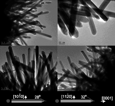 | ||
| Fig. 1 TEM images of ZnO nanorods grown via hydrothermal methods. Adapted from ref. 43 with permission. Copyright American Chemical Society 2003. | ||
Reaction media significantly effects NM growth. Solubility, viscosity, polarity, and surface energy are important parameters to consider when selecting a solvent system. Solubility and polarity directly influence supersaturation, a key parameter for nucleation and crystal growth. Viscosity may affect the mass transport in the reaction. It has been reported that ZnO nanoparticle growth was controlled through the selection of reaction media.44 Strong alkaline conditions can ensure that Zn exists in an ionized state, making it more facile to diffuse to nanocrystal growth fronts in the solvent.
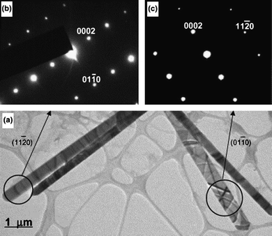
By using various capping agents in the solution synthesis process, the morphology of 1D ZnO NMs can be rationally controlled. In addition to NRs, ZnO nanobelt (NB) morphology via solution synthesis has been reported.46 A solution of ZnSO4, urea, and ethanol was mixed in a Teflon autoclave and the pH was adjusted to 14 by NaOH. The mixture was then reacted at 160 °C for 12 h. Fig. 2 shows a TEM micrograph of the as-synthesized NBs. From the uniform contrast, the authors concluded that the ZnO NMs were NBs rather than NRs. The NBs were 10–20 nm thick and 20–400 nm wide. It is believed that urea selectively adsorbed on certain planes to control the morphology. It is worth mentioning that sulfate ions also can adsorb on nanocrystal surfaces and affect morphology.47 Platelet-like morphology was reported when ZnSO4 was used in conjunction with the hexamethylenetetramine (HMTA) reaction system.48 By combination of adsorption of both urea and sulfate ions, it is possible to synthesize ZnO nanobelts from solution.49
 | ||
| Fig. 2 TEM of as-synthesized ZnO nanobelts. Adapted from ref. 46 with permission. Copyright Elsevier B.V. 2004. | ||
A simple method for directly synthesizing ZnO NRs from Zn powder using cetyltrimethylammonium bromide (CTAB) as an adsorption agent has been reported.50 CTAB was dissolved in an aqueous solution. After adding Zn powder to the CTAB solution under continuous stirring, the resulting suspension was further reacted in a stainless steel autoclave at 180 °C for 24 h. NRs of 1 μm length and 70 nm diameter resulted. The role of CTAB here is different than previous reports. In this case, the surface tension of the solution was likely reduced by the surfactant, allowing for formation of a new phase more easily. Thus, ZnO crystals could form at a relatively low supersaturation. In the literature, the role of CTAB is still under debate. Zhang et al. used CTAB in conjunction with zinc acetate and NaOH as a pH modifier to synthesize ZnO NRs at 120 °C for 20 h.51 The authors argued that CTAB promoted 1D growth since only nanoparticles of 100 nm diameter resulted when no CTAB was used.
In addition to NRs and NBs, ZnO nanotubes (NTs) have also been synthesized in solution.52 To achieve NTs, ZnO NRs were first synthesized at 90 °C from the zinc nitrate and hexamethylenetetramine (HMTA) reaction system and subsequently converted to NTs. Vayssieres et al. explained the NT formation in terms of selective dissolution of the metastable polar (0002) face of the ZnO NR.53 Further investigation of the nanotube growth mechanism using this reaction system is still needed. Hou et al. also reported ZnO NT growth using a hydrothermal method.54 A mixture of zinc acetate, CTAB, and ammonia acting as a pH modifier (pH 10) was reacted at 140 °C for 12 h. The authors proposed different growth mechanisms for tubular and rod formation. For tubular morphology, ZnO seed crystals likely formed from the dehydration of Zn(NH3)42+ under conditions of high ammonia concentration. CTAB likely functioned as a structure directing agent along a preferred direction starting from the seed crystal to directly form NTs. No tubular structures were found when NaOH was substituted for NH3 as the pH modifier indicating that ammonia acted not only as a pH modifier, but also a critical factor for achieving NT morphology. The role of ammonia is not clear yet. CTAB also played a critical role in the tubular morphology since other surfactants such as sodium dodecyl benzene sulfonate (SDBS) and sodium dodecyl sulfate (SDS) did not produce NTs under the same experimental conditions.
2.3. Low temperature wet chemical methods
Other than hydrothermal synthesis of ZnO NMs, which are typically carried out at elevated temperatures and pressures in a Teflon-sealed stainless steel autoclave, mild wet chemical methods at low temperatures (< 100 °C) have been developed.55 The advantages of the lower temperature pathway is obvious: low cost, flexibility, possible in situ investigations, and a wide variety of material compatibility. Recently, the reaction system employing hexamethylenetetramine (HMTA) and soluble zinc salts has been extensively explored to synthesize ZnO NMs. Early reports by Andres et al. showed that HMTA and Zn(NO3)2 or ZnCl2 could be used to synthesize ZnO NRs at temperatures below 100 °C for relatively short reaction periods of c.a. 0.5 h. The authors suggested for the first time that preferential growth along the c-axis was responsible for the 1D morphology.Govender et al. studied solution grown ZnO NR synthesis in detail including factors such as choice of complexing ligand and Zn counter-ion effect.48 It is known that weak bases such as amines hydrolyze in aqueous Zn environments and slowly release hydroxide ions which form various Zn-hydroxide complexes. When ethylenediamine (EN) was used as the weak base, at low zinc concentration and high hydroxide concentration, rod-shape morphology resulted regardless of the Zn counter-ions. When triethanolamine (TEA) was used, only particles and no rods resulted. However, when HMTA was used, high-quality ZnO NRs resulted. The synthesis was successful only at high concentrations of free zinc and low concentrations of hydroxide, contradictory to that of EN as a ligand. The counter-ion effects were also investigated. Zinc salts including acetates, formates, nitrates, perchlorates, and chlorides all resulted in rod-like morphology except zinc sulfate which produced large, flat hexagonal platelets, serving as another piece of evidence for nanobelt growth mentioned earlier.46
HMTA is commonly used in solution-based methods to synthesize ZnO NRs at low temperatures, however its detailed role is still an area of debate in the literature. It is generally accepted that HMTA acts as a pH buffer and slow, steady source of hydroxide ions. The hydroxide ions further react with Zn2+ to form zinc complexes. The decomposition kinetics of HMTA into formaldehyde and ammonia have been investigated and found to be pH dependent.56 Sugunan et al. investigated the role of HMTA in the synthesis of ZnO NRs as well.57 A seeded glass slide was immersed in a chemical bath containing equimolar zinc nitrate and HMTA between 60–95 °C for up to 24 h. FTIR in ATR mode was used to track the decomposition of HMTA by monitoring the changes in absorption due to stretching vibrations of the C–N bond as an indicator of HMTA degradation. Under the experimental conditions, HMTA was expected to slowly decompose to formaldehyde and ammonia, and the C–N bond vibrations measured in the IR spectra were expected to reduce over time. However, the IR spectra taken from the mixture after 1 h reaction was almost identical to that taken after 5 h, strongly suggesting that no change in the tertiary amine structure had taken place. Furthermore, there was no significant difference in NR morphologies that were grown at different temperatures. Thus, the authors hypothesized that the formation of ZnO NRs with high aspect ratios could be explained by preferential adsorption of non-ionic HMTA on the non-polar, a-planes of the ZnO NRs.
Other reaction systems have also been studied to synthesize ZnO nanorods at low temperatures. Polyethylene glycol (PEG) and ammonia were added drop-wise into an aqueous solution of zinc nitrate at room temperature and the final mixture was heated to temperatures ranging from 60 to 90 °C under stirring in an unsealed reactor. It was found that the diameter of the as-synthesized NRs increased with temperature.58 Additionally, ZnO NRs were synthesized from aqueous zinc nitrate and ammonia with zinc metal acting as seeds at temperatures ranging from 60 to 90 °C.28
2.4. Kinetics modeling of 1D ZnO nanomaterial growth in solution
To better understand the growth mechanism of NRs, a quantitative kinetic model is of great importance. Compared to the number of reported NM synthesis methods and property investigations, there are few kinetic studies found in the literature. In a kinetics study, not only the composition and concentration of the products, but also the shape and size need to be determined. Accurate measurements of the nanocrystal diameter can be achieved through TEM observations or light scattering methods. However, obtaining statistical significance of the diameters or length of NMs from TEM observations can be time consuming and cannot be measured in situ. On the other hand, the light scattering technique yields a statistical average of particle sizes. However, particle sizes must be strictly controlled, which is still a synthesis challenge and the measurement assumes spherical particle shape, rendering it inappropriate for 1D NM investigation.The most commonly used model to describe crystal growth is the Lifshitz-Slyozov-Wagner (LSW) model expressed as:
| rn − rn0 = kt | (1) |
Ashfold et al. reported a kinetic investigation of ZnO NR evolution in aqueous media based on the reaction of zinc nitrate and HMTA at 90 °C.61 The zinc ion concentration was determined through both electrochemical analysis and atomic absorption spectroscopy. HMTA concentration was monitored by proton NMR by comparing the integrated value of the HMTA peak area in the NMR spectra to a known predetermined standard. After adding zinc nitrate to solution, the pH decreased from 5.66 to 4.51 and subsequently increased to 5.64 after the first 2 h, and then remained constant indicating that HMTA had acted as a pH buffer. By comparing the measured concentration as a function of pH with the calculated equilibrium concentrations the morphology evolution could be explained by the precipitation mechanism. NRs formed through direct deposition when Zn(OH)2 was a stable intermediate and NTs formed when Zn(OH)2 was thermodynamically unstable under the reaction conditions.
Rao et al. investigated the kinetics of ZnO NR growth in alcoholic media both with and without a polyvinylpyrrolidone (PVP) capping agent.64 The average NR length and diameter were obtained by TEM and SAXS analysis. The NR data from experiments without the capping agent were fit using a r3 Ostwald ripening model indicating a primarily diffusion-controlled growth mechanism. However, for the experiments with the capping agent the data were better fit to a r3 + r2 model, indicating that the growth mechanism involves both diffusion and surface reaction.62
Rather than using the LSW model, Boercker et al. used a dimensionless Thiele modulus to determine the mechanism of ZnO NR growth.65 The Thiele modulus is the ratio of the reaction rate to the diffusion rate, expressed as follows:
 | (2) |
Recently, Zhou and Deng reported a kinetic study of ZnO NR growth from aqueous solution using the zinc acetate and HMTA system reacting at 55-85 °C.67 Equimolar zinc nitrate and HMTA were mixed to obtain a clear solution at room temperature and the beaker was then covered and heated to the desired temperature. The reaction was maintained for t>3 h. Samples were withdrawn from the reactor at different times, filtered through 20 nm filters, and then added to an inductively coupled plasma (ICP) matrix solution containing 5% HCl and 3% HNO3 aqueous solution. Additionally, samples were taken for SEM observation to obtain morphology information. The authors calculated the ZnO NR length as a function of reaction time and it was found that the experimental data fit reasonably well to the models.67 As shown in Fig. 3, the data obtained at low temperatures could be linearly fit, but those at high temperatures significantly deviated. Based on the data, it was hypothesized that HMTA decomposed faster at higher temperatures and thus provided more hydroxide ions, resulting in high supersaturation levels which favor nucleation.68,69
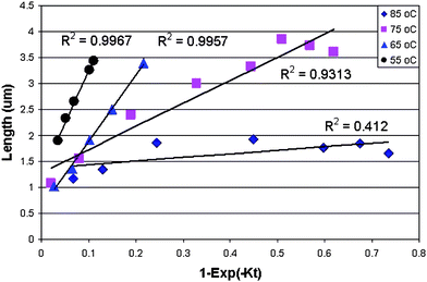 | ||
| Fig. 3 Kinetics of 1D ZnO nanomaterial growth in solution, where K is a constant. Adapted from ref. 67 with permission. Copyright American Chemical Society 2009. | ||
3. Wet chemical method for ZnO nanorod arrays synthesis
3.1. Seeded and unseeded growths of ZnO nanorod arrays
Although high temperature vapor phase methods such as MBE, CVD, PVD, PLD are commonly used for synthesizing high quality ZnO NR arrays, low temperature wet chemical routes have also been successfully developed.70 Typically, substrates with or without seeds are suspended in an aqueous solution of Zn(NO3)2 and C6H12N4 (hexamethylenetetramine, HMTA), and growth occurs at temperatures between 50–95 °C. In general, HMTA, a non-polar molecule, functions as a capping agent on the non-polar facets and impedes the precursor species from reacting thereby promoting one-dimensional growth along the polar facet. Other capping agents such as polyethylenimine, sodium dodecyl sulfate, ethylenediamine promote one-dimensional growth whereas additives such as sodium citrate promote two-dimensional platelet-like growth.One major advantage of using wet chemical growth for fabricating vertical ZnO NR arrays is that virtually any substrate can be used by employing ZnO seeds in the form of thin films or nanoparticles. In this way, the nucleation step is bypassed and only the necessary conditions for growth are considered. Alignment of the ZnO nanocrystals occurs on flat surfaces regardless of their crystallinity or surface chemistry, including ZnO and Al2O3 single crystals, transparent conducting oxides such as indium tin oxide (ITO) and fluorine-doped tin oxide (FTO), amorphous oxides including glass and Si with its native oxide, and the oxide-free metals such as Au and Ti. However, this approach typically requires higher temperature substrate processing. ZnO seeds must be annealed at 150 °C to improve particle adhesion to the substrate and ZnO NR vertical alignment is improved by textured ZnO seeds annealed at 350 °C.71,72 Through the use of seeds, wafer scale synthesis has been achieved.73
ZnO NRs can also be synthesized on organic substrates generally by sputtering ZnO seeds at room temperature on virtually any substrate to guide the high density nanorod growth. For example, T.Y. Liu et al. successfully carried out synthesis on a 4′′ thermoplastic polyurethane substrate.74 The low temperatures and substrate independence are key prerequisites for integrating ZnO into flexible electronic devices. Although more difficult to achieve, there have been reports of ZnO synthesis on polymer substrates such as polydimethylsiloxane (PDMS), polyethylene terepthalate (PET), polyethylene napthalate (PEN), polystyrene (PS), polyurethane, Au-coated polyimide (PI) and PS bead coated polycarbonate (PC).70,75,76 In the case of PDMS, a 5 cm diameter substrate was fully coated with ZnO NRs by employing seeds, but microcracks formed after flexing. Growth on Au-coated PI yielded high density, size-controlled ZnO NRs without using seeds. The alignment of ZnO nanorods grown directly on PC was enhanced by a self-assembled PS sphere monolayer. Qin et al. demonstrated ZnO NW array growth ZnO on flexible Kevlar microfibers with high strength, modulus, toughness and thermal stability.77 Weintraub et al. achieved ZnO NW growth on quartz optical fibers.141
It has been reported that the texture, thickness and crystal size of ZnO seed layers affect the quality of ZnO products.78–81 L.W. Ji et al. reported that the average NW diameter increased from 50 to 130 nm and the NW density decreased from 110 to 60 μm −2 when the thickness of the seed layer varied from 20 to 1000 nm.82 Well vertically-aligned NWs grew on thicker seed layers with good crystallinity while thinner seed layers with poor crystallinity resulted in poor-alignment. S. Baruah and J. Dutta studied the effects of seed size and formation on the growth and orientation of ZnO NRs and found that those grown using zinc acetate-seeded substrates have higher aspect ratios than those grown using nanoparticle-seeded substrates.83 S.F. Wang et al. pointed out that substrates deposited with ZnO seeds with (0002) preferred orientation led to well-defined hexagonal facets (0002) ZnO nanorods grown nearly vertical to the substrates.84
Without the aid of seeds, ZnO NR synthesis can also be carried out on catalysts such as Au, Ag, and Pt. Such metals can even be deposited onto polymeric substrates as thin films to achieve NR growth. In this case, the surface roughness of the thin film must be carefully controlled to promote nucleation. In addition, the NR orientation is largely a function of the surface topography. In order to achieve vertically-aligned NRs, an appropriate process flow must be employed for smooth substrate surfaces.
3.2. Position, density, and length control of ZnO nanorod arrays
Weintraub et al. reported the site-selective growth of individual ZnO NRs in patterned arrays by a wet chemical approach on organic substrates.89 This novel synthesis technique does not require a ZnO thin film or nanoparticle seeds and it can be carried out at low temperatures (<70 °C) making it an important synthesis technique for flexible electronic applications. The process is schematically shown in Fig. 4. The substrate was a 50 μm thick Kapton polyimide film provided by Du Pont (HN200). A thin layer of Au was thermally evaporated to provide electrical conductivity and uniform nucleation sites on the substrate. The substrate was then spin coated with PMMA resist and arrays of circular patterns (diameters of 200 nm) were patterned into the resist using a LEO 1550 field emission scanning electron microscope (FESEM) modified with a J.C. Nabity Nanometer Pattern Generation System (NPGS). The substrates were developed in a 3:1 by volume isopropyl alcohol/methyl isobutyl ketone solution to reveal the patterned features. Electrical contact was made to the substrate by selectively removing a small portion of the PMMA resist using acetone.
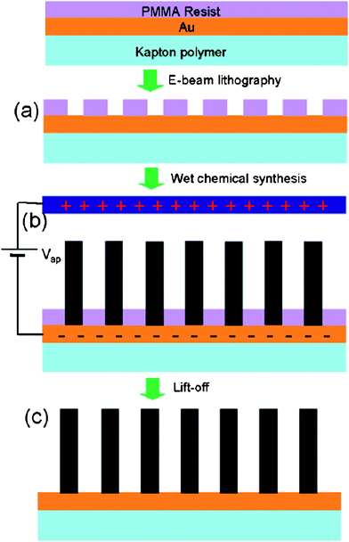 | ||
| Fig. 4 Process flow for lithography-based position-controlled ZnO nanorod array growth. Flexible Kapton polymer substrate is coated in a Au thin film and PMMA resist. (a) Desired density is defined using electron beam lithography, and the Au pattern is subsequently exposed during the developing step. (b) The patterned substrate is immersed in a nutrient solution bath and held at a −500 mV bias relative to the reference electrode. (c) The PMMA resist is finally removed in the lift-off step. Adapted from ref. 89 with permission. Copyright American Chemical Society 2007. | ||
The patterned substrate was submerged vertically into a nutrient solution parallel to a second Au coated Kapton substrate of equal dimensions referred to as the reference electrode. A −500 mV potential was applied relative the patterned substrate using a DC power supply. The aqueous nutrient solution was composed of 20 mM zinc nitrate hexahydrate and 20 mM hexaminetetramine (HMTA) and maintained at 70 ± 5 °C on a hot plate. The reaction time was varied between 1–5 h in order to control the NR length. Once the synthesis was complete, the PMMA resist was removed with acetone, the sample was rinsed with DI water and air dried overnight. Fig. 5a shows a low magnification SEM image of a large array of individual ZnO nanorods separated by 535 nm. Circular patterns of 200 nm were defined in the resist in order to nucleate a single ZnO NR. ZnO NRs did not grow on the PMMA resist regions due to a lack of nucleation sites. It was found that 200 nm was the optimum circular diameter in order to nucleate a single NR under the given experimental conditions. At 70 °C, the approximate growth rate was 0.7 μm/h. The NR length was controlled by the synthesis time. Fig. 5b shows a high magnification top SEM image of the ZnO NR array showing the hexagonal cross section and well-defined facets and demonstrates that the NRs exhibit a high degree of vertical alignment. The base diameter was defined by the resist mask. Above the resist, lateral growth occurred along the non-polar {2 0} planes resulting in NRs with a diameter of 300 ± 50 nm. Fig. 5b inset shows an optical micrograph of the patterned ZnO NR array appearing green due to periodic spacing of 535 nm.
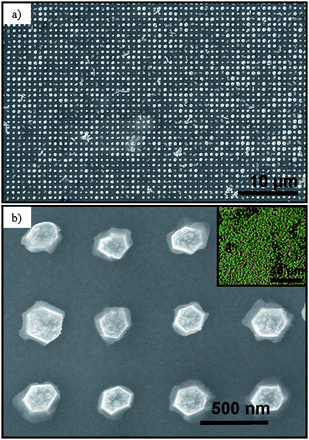 | ||
| Fig. 5 SEM images of large-scale ZnO nanorod array (a) low magnification and (b) high magnification. Inset is the optical micrograph of large-scale patterned ZnO nanorod array appearing green due to periodic spacing of 535 nm. Adapted from ref. 89 with permission. Copyright American Chemical Society 2007. | ||
Si substrates with dimensions of 1 cm × 1 cm were deposited with a 100 nm ZnO seed film by RF magnetron sputtering. To establish the ion transport barrier, the ZnO seed-coated samples were spin-coated with alternating layers of poly(allylamine hydrochloride) (PAH) and poly(sodium 4-styrenesulfonate) (PSS) polymers. Samples of 0, 1, 2, 3, 4, and 5 bilayers were prepared. AFM analysis verified the film thicknesses and showed in general that each polymer bilayer measured 2.5 nm. For solution-based NR array synthesis, the substrates were floated face-down in a 50 ml Pyrex glass bottle containing a 20 mM solution of zinc nitrate hexahydrate and hexamethylenetetramine (HMTA) and aged for 1.5 h at 90 °C in a laboratory grade box oven. Substrates were subsequently rinsed with water and ethanol and oven dried at 60 °C for 30 mins in air.
Fig. 6 displays the representative SEM images of the density-controlled ZnO NR arrays for the 0, 1, 3, and 5 bilayer samples showing the general trend of decreasing density. As expected in Fig. 6 (a), the sample without a polymer barrier exhibits the highest density. Likewise, the density decreases as the number of polymer bilayers increases, as shown in Fig. 6(b–d) corresponding to 1, 3, and 5 bilayer samples, respectively. Fig. 6 insets show high magnification SEM images of the morphology. It can be seen that the NRs become tapered for the polymer-coated samples. It is believed that the polymer layer effectively slowed the initial NR growth kinetics. As the polymer layer increased to 5 layers (Fig. 6d), instead of NR growth, some ZnO particles precipitated out on the substrate and in the solution due to the migration of some ZnO precursor ions through the barrier polymer film. As the reaction sequence proceeds, the available ZnO precursor ions began to decrease and the net effect was a morphological NR tapering. It was also observed that the NR shape changed from regular rod with a flat top to a sharp pencil shape. The rod size and length distributions were also increased when the number of the polymer thin layer was increased. Quantitative analysis was carried out to determine the relationship between both the NR density and tip diameter and the number of polymer bilayers as shown in Fig. 7a. The density was uniform throughout the 1 cm × 1 cm substrate. NR average density was calculated by counting the number of NRs shown in SEM images of the same magnification at three different substrate locations chosen at random. As shown in Fig. 7a, the average NR density decreases exponentially with values of 123, 48, 11, 7, 2, and 1 NR/μm2 corresponding to 0, 1, 2, 3, 4, and 5 polymer bilayers. The average NR tip diameter, estimated by measuring the tip diameter of 20 NRs chosen at random imaged using high magnification SEM, indicates that although the base diameter increased, the tip diameter change is not significant, as shown in Fig. 7a. NRs in the various samples ranged in length from ca. 0.2–2 μm. X-ray diffraction data shown in Fig. 8b confirm the epitaxial nature of the aligned NRs with the seeds as well the (001) fast growth direction. The two strong peaks seen at 33.0° and 34.4° correspond to the substrate Si (200) and ZnO (002) planes. The presence of only a single ZnO (002) peak indicates a high degree of vertical alignment. Weak peaks at 31.8° and 36.3°, present only in the case of the 5 bilayer sample, correspond to ZnO (100) and ZnO (101) reflections and indicate that this sample had poor vertical alignment.
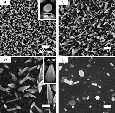 | ||
| Fig. 6 Top view: SEM micrographs, at the same magnification, of ZnO nanorod arrays with substrates having a varying number of PSS/PAS bilayers: (a) 0 bilayers (inset shows nanorod morphology); (b) 1 bilayer; (c) 3 bilayers (inset shows nanorod morphology); (d) 5 bilayers. Adapted from ref. 90 with permission. Copyright IOP Publishing Ltd 2008. | ||
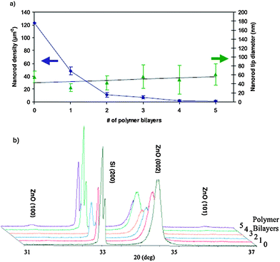 | ||
| Fig. 7 (a) Plot of nanorod density and nanorod tip diameter as a function of the number of LBL polymer bilayers. (b) X-ray diffraction spectra for the samples with differing numbers of polymer bilayers. Adapted from ref. 90 with permission. Copyright IOP Publishing Ltd 2008. | ||
 0] surfaces of single crystal ZnO substrates using e-beam lithography.163
4. Applications of solution synthesized one-dimensional ZnO nanostructures
Due to the unique electrical and optical properties of ZnO, its applications have been expanding rapidly in recent years. In this review, we will focus mainly on the recent application developments of 1D ZnO NMs synthesized by solution methods. In particular, we will cover applications such as sensors, field emission devices, photodetectors, optical switches, and solar cells.4.1. Sensors
The mechanism behind ZnO gas sensors is usually described by the change of electrical properties induced by the adsorption of gas molecules on the surface of ZnO.108,109 In general, ZnO is an intrinsically n-type semiconductor due to oxygen vacancies acting as electron donors which supply electrons to the conduction band. In ambient air, some oxygen molecules will adsorb on the surface of the ZnO and subsequently be reduced to oxygen ions (O2−, O−, and O2−) by capturing electrons from the ZnO conduction band, resulting in an increased electrical resistance.110 When exposed to a reductive gas environment at moderate temperatures, the gas reacts with the adsorbed oxygen ions, releasing the trapped electrons back to the conduction band, thereby leading to an increased carrier concentration. Consequently, the resistance decreases under exposure to reductive gases such as ethanol, acetone, ammonia, carbon monoxide, and hydrogen.109,111 However, the mechanism may vary depending on the different properties of gases and ZnO NM morphologies. For example, in the case of H2S, the response cannot be explained solely by surface adsorption because the transformation of highly resistive ZnO into well-conducting ZnS leads to an increase in conductivity.103 Wang et al. reported a hydrothermally-synthesized ZnO NT array-based gas sensor which exhibited NO2 sensitivity at low temperatures of 30 °C.112 This was attributed to temperature-dependent and concentration-dependent ZnO NT n–p transition behaviors. Gigantic enhancement in CO sensitivity was achieved using a schottky-contacted ZnO nanowire sensor.142 The authors proposed that the mechanism relied on the responsive variation of the surface chemisorbed gases and the amplification role played by the nanowire on the schottky barrier height.
The surface electrical charge density or electrode potential of ZnO will change with pH in electrolyte.120,121 Based on this principle, ZnO nanorods were used to fabricate a highly sensitive pH sensor on Ag-coated borosilicate glass Femtotio® II capillaries to detect the intracellular pH of a human fat cell.120 Water et al. successfully used solution-grown ZnO NR arrays to enhance the sensitivity of a Love wave liquid sensor.122 It was found that ZnO NRs of moderate length could increase the interaction between the propagating acoustic wave and surface perturbations of a liquid, resulting in an enhancement in sensitivity.
4.2. Field emission devices
Since the discovery that carbon nanotubes (NTs) could function as efficient field emitters,123–125 research efforts have progressed towards other 1D NMs such as metal oxides motivated by their low work functions, high aspect ratios, high mechanical stabilities and conductivities.126,127 In particular, 1D ZnO NR arrays have received significant attention because of their simple and low-cost processing made possible by solution synthesis.128,129 Liu et al. used Zn foil as a substrate to grow ZnO NR arrays by a hydrothermal reaction.129 The field emission electrical data exhibited a two-stage slope behavior with an estimated field emission enhancement factor (β) of 8504 at lower applied voltages and 1581 at higher voltages.For a given material, it has been shown that the field emission efficiency can be improved by controlling the emitter density and aspect ratio.130–132 Emitters that are too closely packed suffer from a screening effect, whereas emitters spaced too far apart approach the behavior of a thin film.127,133 Therefore, it is expected that there is an optimal density for achieving the best field emission performance. Weintraub et al. have employed a simple, scalable, and cost-effective solution-based method for controlling the ZnO NR array density and morphology to optimize the field emission performance.90 The field emission results revealed that an emitter density of 7 NRs μm−2 and a tapered NR morphology generated a high field enhancement factor of 5884 with a low turn-on field of 5.1 V μm−1.
4.3. Photodetectors and optical switches
The conductivity of ZnO, a wide band gap semiconductor (Eg 3.3 eV), is extremely sensitive to UV irradiation. Therefore, ZnO NMs have been regarded as one of the most promising materials for nanoscale UV photodetectors,134 UV laser diodes135 and other nanoscale optoelectronic devices. 1D ZnO NMs have received particular attention as high sensitivity photodetectors.136,137,60The photoconduction mechanism for nanoscale ZnO has been widely studied.138,139 Upon exposure to air, oxygen molecules adsorb on the ZnO surface and capture free electrons from the ZnO conduction band, thereby transforming to oxygen ions (O2−, O−, and O2−) by the following reaction: O2(g) + e− = O2−(ad), which creates a high-resistance depletion layer near the surface. Upon illumination by photon energies above the semiconductor band gap, e− − h+ pairs are photogenerated according to hν = e− + h+. The h+ migrate to the surface where they are neutralized by negatively charged surface oxygen ions such as O2−(ad) +h+ = O2(g). As a result, unpaired electrons are produced, which contribute to the increase in conductivity. Fig. 9 schematically demonstrates the photoconduction mechanism in the presence of high density hole-trap states at the ZnO NW surface.139
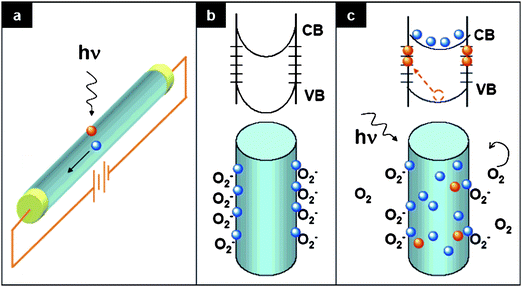 | ||
| Fig. 9 Photoconduction in nanowire photodetectors. (a) Schematic of a nanowire photoconductor. (b and c) Trapping and photoconduction mechanism in ZnO nanowires in dark (b) and under UV illumination (c): the top drawing shows the schematic of the energy band diagrams; the bottom drawing shows oxygen molecules adsorption or desorption state. Adapted from ref. 139 with permission. Copyright American Chemical Society 2007. | ||
4.4. Solar cells
1D NMs will play a large role in realizing 3rd generation photovoltaic (PV) devices which seek to maximize conversion efficiencies while minimizing processing costs to achieve the $1/watt goal which represents the economic benchmark when PV is cost competitive with fossil fuel energy sources. Among the various 3rd generation PV approaches such as all organic and multijunction, dye-sensitized solar cells (DSSCs) are promising because of their low processing costs and moderate efficiencies. DSSCs are photovoltaic devices in which light absorption and charge carrier transport are controlled separately. A photosensitizing dye anchored to a high surface area wide bandgap semiconductor absorbs the light while photogenerated electrons are transported through the semiconductor and holes through a redox electrolyte. Compared to traditionally TiO2 nanoparticle films, ZnO NW arrays are considered promising photoanode material alternatives because of their highly controllable 1D single-crystalline nanoscale morphology which can provide direct electron transport pathways for photogenerated electrons. Well-oriented, high aspect ratio crystalline ZnO NWs were synthesized by hydrothermally and DSSCs were fabricated.140 The high crystallinity and internal electric field resulted in good electron transport within the nanowire photoanode and effective carrier collection. At 1 sun illumination intensity, the ZnO NW DSSC yielded the following performance: short-circuit current density (Jsc) 5.3–5.85 mA cm−2, open circuit voltage (Voc) 0.61–0.71 V, fill factor (FF) 0.36–0.38 and total efficiency (η) 1.2–1.5%. The overall conversion efficiency was limited primarily by low NW surface area which reduces dye loading. To increase the interaction between the incoming photons and the light absorbing dye, Weintraub et al. recently reported a three-dimensional approach based on a ZnO nanowire-optical fiber hybrid structure.141 The concept is shown in Fig. 10. The ZnO nanowires, grown normal to the optical fiber surface via an aqueous solution-based approach, enhance the surface area for the interaction of light with dye molecules. The light illuminates the fiber from one end along the axial direction, and its internal reflection within the fiber creates multiple opportunities for energy conversion at the interfaces. Using an optical fiber with a rectangular geometry, the performance under one full sun intensity (AM 1.5 illumination, 100 mW cm−2) yielded the following: Jsc = 9.5 mA cm−2, Voc = 0.559 V, FF = 0.623, η = 3.3%. Without increasing the film thickness, the photon-dye interaction was significantly enhanced yielding superior overall energy conversion efficiency. The type and properties of dyes affect the DSSC performance. Wu et al. studied the effects of dye adsorption on the electron transport properties in ZnO-nanowire DSSCs and suggested that the mercurochrome dyes are more appropriate than ruthenium complex dyes because N3-sensitized ZnO photoanodes exhibited a higher surface trap density.143 Recently, He et al. investigated the electron transport and recombination properties of hydrothermally-synthesized ZnO nanorod based DSSCs using electrochemical impedance spectroscopy (EIS).144 They pointed out that the recombination at the ZnO-electrolyte interface occurs via electron transfer from surface trap states and device performance is greatly influenced by the variation of recombination properties as a function of illumination intensity.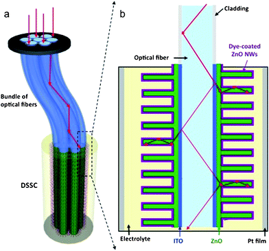 | ||
| Fig. 10 Design and principle of a three-dimensional DSSC. a) The 3D DSSC is composed of optical fibers and ZnO nanowires grown vertically on the fiber surface via an aqueous solution method. b) Detailed structure of the 3D DSSC. Adapted from ref. 141 with permission. Copyright Wiley-VCH Verlag GmbH & Co. KGaA, Weinheim 2009. | ||
Hybrid photovoltaic devices consisting of a π–conjugated polymer and a metal oxide semiconductor have also attracted significant attention. Olson et al. fabricated hybrid photovoltaic devices by infiltrating poly(3-hexylthiophene) (P3HT) or P3HT/(6,6)-phenyl C61 butyric acid methyl ester (PCBM) into solution-synthesized ZnO nanofibers.145Fig.11 shows a schematic diagram of an ideal ZnO nanorod/conjugated polymer photovoltaic device.145 The influence of ZnO surface processing was found to be critical for the performance of ZnO/P3HT devices.146
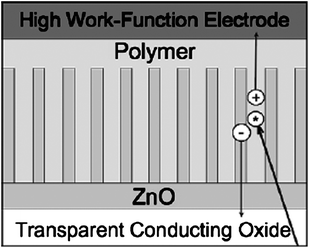 | ||
| Fig. 11 Schematic diagram of an ideal nanostructured oxide/conjugated polymer photovoltaic device. Adapted from ref. 145 with permission. Copyright Elsevier B.V. 2005. | ||
Due to its wide band gap, ZnO cannot absorb in the visible region of the solar spectrum (> 420 nm). Therefore, hybrid ZnO solar cell devices employing organic dye molecules,147 inorganic quantum dots148 and nanoparticles149 which effectively absorb in the visible and IR regions are of interest for efficient energy harvesting. Thitima et al. compared the charge injection efficiency of hybrid P3HT/PCBM/ZnO solar cells processed with and without N719 dye and found that both the short circuit current density and the efficiency were higher with the dye.147 Leschkies et al. reported a CdSe quantum dot-sensitized ZnO nanowire solar cell as shown schematically in fig. 12.148 The photocurrent generated from the visible light was due to the electron-hole pairs created in the CdSe quantum dots, followed by electron injection into the ZnO nanowires. Chen et al. reported a Au nanoparticle-sensitized ZnO nanorod solar cell.149 The Au nanoparticles enhanced the absorption of visible light through surface plasmon resonance and the schottky barrier at the ZnO/Au interface reduced electron-hole recombination, which ultimately led to improved efficiency. Others have fabricated core-shell heterostructures to optimize surface chemistry.150,151 For example, Plank et al. fabricated ZnO-MgO core-shell based solid-state DSSCs and observed a five-fold efficiency improvement compared to pristine ZnO nanowire based photovoltaic devices.150 Greene et al. found that the efficiency of P3HT/ZnO nanorod solar cells could be improved five-fold by a thin TiO2 shell on the ZnO nanorod arrays.151 Enhancing light coupling into the active region of the photovoltaic devices is another way to improve efficiency by adding anti-reflective coatings to minimize reflectance losses. ZnO is regarded as a good dielectric anti-reflective coating material due to its high transparency and appropriate refractive index (n = 2). Lee et al. employed solution-synthesized ZnO nanorod arrays as efficient solar cell anti-reflective coatings to enhance solar cell performance.152
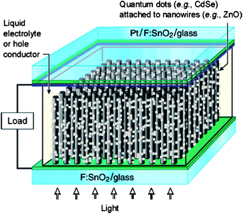 | ||
| Fig. 12 Schematic of the quantum-dot-sensitized solar cell. Adapted from ref. 148 with permission. Copyright American Chemical Society 2007. | ||
Flexible solar cells based on nanostructured metal oxides have attracted increasing interest due to the potentially light weight, thin, and bendable advantages. Jiang et al. reported a dye-sensitized solar cell based on hydrothermally grown ZnO nanowire films on flexible PET/ITO substrates.153 ZnO nanoparticles were attached to the ZnO nanowire surface to further increase the surface area and results showed promising device stability.
Concurrent harvesting of multiple types of energies is of critical significance for long-term energy needs. Chen et al. reported a hybrid cell that simultaneously harvests solar and mechanical energies.154Fig.13 shows the schematic structure of the serially hybrid cell. A hydrothermally-grown ZnO NW-based DSSC was built on the top surface to convert solar energy, and a piezoelectric nanogenerator was built on the bottom surface to convert ultrasonic wave energy. The two energy harvesting approaches could work simultaneously or individually, and could be integrated in parallel as well as in serial, which can be an effective way to utilize energy resources.
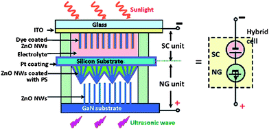 | ||
| Fig. 13 Schematic structure of a serially integrated hybrid cell (HC), illuminated by sunlight from the top and excited by an ultrasonic wave from the bottom. The ITO layer on the solar cell (SC) unit and GaN substrate are defined as the cathode and anode of the HC, respectively. The symbol to represent the HC is shown at the right-hand side. Adapted from ref. 154 with permission. Copyright American Chemical Society 2009. | ||
5. Conclusions and future outlook
Owing to its unique properties, one-dimensional ZnO nanomaterials have great potential applications in nanogenerators,34,155,156 photocatalysis,157 surface acoustic waveguides,158 humidity sensors159,160 as well as in sensors, solar cells, and field emission devices. In addition, the applications can be expanded by surface functionalization or by coupling the different properties of semiconducting and piezoelectric ZnO. Wet chemistry is a simple method for synthesizing large scale one-dimensional ZnO nanowire arrays. The position, diameter, density and length of the ZnO arrays can be rationally controlled through optimizing the synthesis parameters to improve the performance of ZnO NM-based devices. Further research is needed to improve the quality of ZnO nanowire arrays and take advantage of the cost-effective solution route to extent their applications.Acknowledgements
BW thanks IPST at Georgia Tech for the fellowship.References
- X. Michalet, F. F. Pinaud, L. A. Bentolila, J. M. Tsay, S. Doose, J. J. Li, G. Sundaresan, A. M. Wu, S. S. Gambhir and S. Weisset, Science, 2005, 307, 538 CrossRef CAS.
- B. Dubertret, P. Skourides, D. J. Norris, V. Noireaux, Ali H. Brivanlou and A. Libchaber, Science, 2002, 298, 1759 CrossRef CAS.
- D. E. Aspnes, Thin Solid Films, 1982, 89, 249 CrossRef CAS.
- J. C. Francois, Y. Massiani, P. Gravier, J. Grimblot and L. Gengembre, Thin Solid Films, 1993, 223, 223 CrossRef CAS.
- J. E. Gray and B. Luan, J. Alloys Compd., 2002, 336, 88 CrossRef CAS.
- M. Stratmann, R. Feser and A. Leng, Electrochim. Acta, 1994, 39, 1207 CrossRef CAS.
- U. Scherf and E. J. W. List, Adv. Mater., 2002, 14, 477 CrossRef CAS.
- C. D. Dimitrakopoulos and P. R. L. Malenfant, Adv. Mater., 2002, 14, 99 CrossRef CAS.
- S. A. Wolf, D. D. Awschalom, R. A. Buhrman, J. M. Daughton, S. von Molnar, M. L. Roukes, A. Y. Chtchelkanova and D. M. Treger, Science, 2001, 294, 1488 CrossRef CAS.
- S. Lijima, Nature, 1991, 354, 56 CrossRef CAS.
- T. W. E. P. M. Ajayan, T. Ichihashi, S. lijima, K. Tanigaki and H. Hiura, Nature, 1993, 362, 522 CrossRef CAS.
- A. M. Morales and C. M. Lieber, Science, 1998, 279, 208 CrossRef CAS.
- J. T. Hu, T. W. Odom and C. M. Lieber, Acc. Chem. Res., 1999, 32, 435 CrossRef CAS.
- X. Duan and C. M. Lieber, Adv. Mater., 2000, 12, 298 CrossRef CAS.
- J. D. Holmes, K. P. Johnston, R. C. Doty and B. A. Korgel, Science, 2000, 287, 1471 CrossRef CAS.
- C. J. Murphy and N. R. Jana, Adv. Mater., 2002, 14, 80 CrossRef CAS.
- Y. D. Li, H. W. Liao, Y. Ding, Y. T. Qian, L. Yang and G. E. Zhou, Chem. Mater., 1998, 10, 2301 CrossRef CAS.
- Z. W. Pan, Z. R. Dai and Z. L. Wang, Science, 2001, 291, 1947 CrossRef CAS.
- Z. L. Wang, Adv. Mater., 2003, 15, 432 CrossRef CAS.
- G. Schider, J. R. Krenn, W. Gotschy, B. Lamprecht, H. Ditlbacher, A. Leitner and F. R. Aussenegg, J. Appl. Phys., 2001, 90, 3825 CrossRef CAS.
- Q. H. Li, Q. Wan, Y. X. Liang and T. H. Wang, Appl. Phys. Lett., 2004, 84, 4556 CrossRef CAS.
- X. Sun, H. Zhang, J. Xu, Q. Zhao, R. Wang and D. Yu, Solid State Commun., 2004, 129, 803 CrossRef CAS.
- M. Wang, C. H. Ye, Y. Zhang, G. M. Hua, H. X. Wang, M. G. Kong and L. D. Zhang, J. Cryst. Growth, 2006, 291, 334 CrossRef CAS.
- D. Li and Y. N. Xia, Nano Lett., 2003, 3, 555 CrossRef CAS.
- T. Thurn-Albrecht, J. Schotter, C. A. Kastle, N. Emley, T. Shibauchi, L. Krusin-Elbaum, K. Guarini, C. T. Black, M. T. Tuominen and T. P. Russell, Science, 2000, 290, 2126 CrossRef CAS.
- P. D. Cozzoli, A. Kornowski and H. Weller, J. Am. Chem. Soc., 2003, 125, 14539 CrossRef CAS.
- M. Wang, C. H. Ye, Y. Zhang, H. X. Wang, X. Y. Zeng and L. D. Zhang, J. Mater. Sci.: Mater. Electron., 2008, 19, 211 CrossRef CAS.
- Y. Tak and K. J. Yong, J. Phys. Chem. B, 2005, 109, 19263 CrossRef CAS.
- Y. P. Rakovich, Y. Volkov, S. Sapra, A. S. Susha, M. Doblinger, J. F. Donegan and A. L. Rogach, J. Phys. Chem. C, 2007, 111, 18927 CrossRef CAS.
- Z. Y. Wang, J. Hu, A. P. Suryavanshi, K. Yum and M. F. Yu, Nano Lett., 2007, 7, 2966 CrossRef CAS.
- Z. Zhou, Q. Sun, Z. Hu and Y. Deng, J. Phys. Chem. B, 2006, 110, 13387 CrossRef CAS.
- Q. Wan, Q. H. Li, Y. J. Chen, T. H. Wang, X. L. He, J. P. Li and C. L. Lin, Appl. Phys. Lett., 2004, 84, 3654 CrossRef CAS.
- Z. Y. Fan, D. W. Wang, P. C. Chang, W. Y. Tseng and J. G. Lu, Appl. Phys. Lett., 2004, 85, 5923 CrossRef CAS.
- Z. L. Wang and J. Song, Science, 2006, 312, 243.
- Z. L. Wang, J. Phys.: Condens. Matter, 2004, 16, R829 CrossRef CAS.
- U. Ozgur, Y. I. Alivov, C. Liu, A. Teke, M. A. Reshchikov, S. Dogan, V. Avrutin, S. J. Cho and H. Morkoc, J. Appl. Phys., 2005, 98, 041301 CrossRef.
- Z. L. Wang, Mater. Sci. Eng., B, 2009, R64, 33 CAS.
- J. Zhang, L. D. Sun, H. Y. Pan, C. S. Liao and C. H. Yan, New J. Chem., 2002, 26, 33 RSC.
- Z. R. Tian, J. A. Voigt, J. Liu, B. Mckenzie, M. J. Mcdermott, M. A. Rodriguez, H. Konishi and H. Xu, Nat. Mater., 2003, 2, 821 CrossRef CAS.
- L. Guo, Y. L. Ji, H. B. Xu, P. Simon and Z. Y. Wu, J. Am. Chem. Soc., 2002, 124, 14864 CrossRef CAS.
- J. M. Wang and L. Gao, J. Mater. Chem., 2003, 13, 2551 RSC.
- H. M. Hu, X. H. Huang, C. H. Deng, X. Y. Chen and Y. T. Qian, Mater. Chem. Phys., 2007, 106, 58 CrossRef CAS.
- B. Liu and H. C. Zeng, J. Am. Chem. Soc., 2003, 125, 4430 CrossRef CAS.
- Z. S. Hu, G. Oskam and P. C. Searson, J. Colloid Interface Sci., 2003, 263, 454 CrossRef CAS.
- T. Yoshida, M. Tochimoto, D. Schlettwein, D. Wohrle, T. Sugiura and H. Minoura, Chem. Mater., 1999, 11, 2657 CrossRef CAS.
- X. Y. Zhang, J. Y. Dai, H. C. Ong, N. Wang, H. L. W. Chan and C. L. Choy, Chem. Phys. Lett., 2004, 393, 17 CrossRef CAS.
- A. Degen and M. Kosec, J. Eur. Ceram. Soc., 2000, 20, 667 CrossRef CAS.
- K. Govender, D. S. Boyle, P. B. Kenway and P. O'Brien, J. Mater. Chem., 2004, 14, 2575 RSC.
- E. E. Abd El Aal, Corros. Sci., 2000, 42, 1 CrossRef.
- X. M. Sun, X. Chen, Z. X. Deng and Y. D. Li, Mater. Chem. Phys., 2003, 78, 99 CrossRef.
- H. Zhang, D. Yang, Y. J. Ji, X. Y. Ma, J. Xu and D. L. Que, J. Phys. Chem. B, 2004, 108, 3955 CrossRef CAS.
- Y. Sun, G. M. Fuge, N. A. Fox, D. J. Riley and M. N. R. Ashfold, Adv. Mater., 2005, 17, 2477 CrossRef CAS.
- L. Vayssieres, K. Keis, A. Hagfeldt and S. E. Lindquist, Chem. Mater., 2001, 13, 4395 CrossRef CAS.
- H. W. Hou, Y. Xie and Q. Li, Solid State Sci., 2005, 7, 45 CrossRef CAS.
- M. A. Verges, A. Mifsud and C. J. Serna, J. Chem. Soc., 1990, 86, 959 Search PubMed.
- J. G. Strom and H. W. Jun, J. Pharm. Sci., 1980, 69, 1261 CAS.
- A. Sugunan, H. C. Warad, M. Boman and J. Dutta, J. Sol–Gel Sci. Technol., 2006, 39, 49 CrossRef CAS.
- H. X. Zhang, J. Feng, J. Wang and M. L. Zhang, Mater. Lett., 2007, 61, 5202 CrossRef CAS.
- J. J. Qiu, X. M. Li, W. Z. He, S. J. Park, H. K. Kim, Y. H. Hwang, J. H. Lee and Y. D. Kim, Nanotechnology, 2009, 20, 15.
- J. Zhou, Y. D. Gu, Y. F. Hu, W. J. Mai, P. H. Yeh, G. Bao, A. K. Sood, D. L. Polla and Z. L. Wang, Appl. Phys. Lett., 2009, 94, 191103 CrossRef.
- M. N. R. Ashfold, R. P. Doherty, N. G. Ndifor-Angwafor, D. J. Riley and Y. Sun, Thin Solid Films, 2007, 515, 8679 CrossRef CAS.
- R. Viswanatha, P. K. Santra, C. Dasgupta and D. D. Sarma, Phys. Rev. Lett., 2007, 98, 255501 CrossRef.
- B. Wen, Y. Huang and J. J. Boland, J. Phys. Chem. C, 2008, 112, 106 CrossRef CAS.
- K. Biswas, B. Das and C. N. R. Rao, J. Phys. Chem. C, 2008, 112, 2404 CrossRef CAS.
- J. E. Boercker, J. B. Schmidt and E. S. Aydil, Cryst. Growth Des., 2009, 9, 2783 CrossRef CAS.
- L. Vayssieres, Adv. Mater., 2003, 15, 464 CrossRef CAS.
- Z. Z. Zhou and Y. L. Deng, J. Phys. Chem. C, 2009, 113, 19853 CrossRef CAS.
- T. Sugimoto, Adv. Colloid Interface Sci., 1987, 28, 65 CAS.
- V. K. Lamer and R. H. Dinegar, J. Am. Chem. Soc., 1950, 72, 4847 CrossRef CAS.
- B. D. Yuhas, D. O. Zitoun, P. J. Pauzauskie, R. He and P. Yang, Angew. Chem., Int. Ed., 2006, 45, 420 CrossRef CAS.
- L. E. Greene, M. Law, J. Goldberger, F. Kim, J. C. Johnson, Y. F. Zhang, R. J. Saykally and P. D. Yang, Angew. Chem., Int. Ed., 2003, 42, 3031 CrossRef CAS.
- L. E. Greene, M. Law, D. H. Tan, M. Montano, J. Goldberger, G. Somorjai and P. D. Yang, Nano Lett., 2005, 5, 1231 CrossRef CAS.
- A. Nadarajah, R. C. Word, J. Meiss and R. Konenkamp, Nano Lett., 2008, 8, 534 CrossRef CAS.
- T. Y. Liu, H. C. Liao, C. C. Lin, S. H. Hu and S. Y. Chen, Langmuir, 2006, 22, 5804 CrossRef CAS.
- P. X. Gao, J. H. Song, J. Liu and Z. L. Wang, Adv. Mater., 2007, 19, 67 CrossRef CAS.
- C. C. Lin, S. Y. Chen and S. Y. Cheng, J. Cryst. Growth, 2005, 283, 141 CrossRef CAS.
- Y. Qin, X. D. Wang and Z. L. Wang, Nature, 2008, 451, 809 CrossRef CAS.
- J. Song and S. Lim, J. Phys. Chem. C, 2007, 111, 596 CrossRef CAS.
- J. Liu, J. She, S. Deng, J. Chen and N. Xu, J. Phys. Chem. C, 2008, 112, 11685 CrossRef CAS.
- G. Kenanakis, D. Vernardou, E. Koudoumas and N. Katsarakis, J. Cryst. Growth, 2009, 311, 4799 CrossRef CAS.
- W. Y. Wu, C. C. Yeh and J. M. Ting, J. Am. Ceram. Soc., 2009, 92, 2718 CrossRef CAS.
- L. W. Ji, S. M. Peng, J. S. Wu, W. S. Shih, C. Z. Wu and I-Tseng Tang, J. Phys. Chem. Solids, 2009, 70, 1359 CrossRef CAS.
- S. Baruah and J. Dutta, J. Sol–Gel Sci. Technol., 2009, 50, 456 CrossRef CAS.
- S. F. Wang, T. Y. Tseng, Y. R. Wang, C. Y. Wang and H. C. Lu, Ceram. Int., 2009, 35, 1255 CrossRef CAS.
- X. D. Wang, C. J. Summers and Z. L. Wang, Nano Lett., 2004, 4, 423 CrossRef CAS.
- Y. J. Kim, C. H. Lee, Y. J. Hong, G. C. Yi, S. S. Kim and H. Cheong, Appl. Phys. Lett., 2006, 89, 163128 CrossRef.
- B. S. Kang, S. J. Pearton and F. Ren, Appl. Phys. Lett., 2007, 90, 083104 CrossRef.
- T. Sounart, J. Liu, J. Voigt, J. Hsu, E. Spoerke, Z. R. Tian and Y. Jiang, Adv. Funct. Mater., 2006, 16, 335 CrossRef CAS.
- B. Weintraub, Y. L. Deng and Z. L. Wang, J. Phys. Chem. C, 2007, 111, 10162 CrossRef CAS.
- B. Weintraub, S. Chang, S. Singamaneni, W. H. Han, Y. J. Choi, J. Bae, M. Kirkham, V. V. Tsukruk and Y. Deng, Nanotechnology, 2008, 19, 435302 CrossRef.
- Y. Li, F. D. Valle, M. Simonnet, I. Yamada and J. J. Delaunay, Nanotechnology, 2009, 20, 045501 CrossRef.
- Tz-J. Kuo, C. N. Lin, C. L. Kuo and M. H. Huang, Chem. Mater., 2007, 19, 5143 CrossRef CAS.
- N. Zhang, K. Yu, L. Li and Z. Zhu, Appl. Surf. Sci., 2008, 254, 5736 CrossRef CAS.
- G. Hua, Y. Zhang, J. Zhang, X. Cao, W. Xu and L. Zhang, Mater. Lett., 2008, 62, 4109 CrossRef CAS.
- T. Seiyama, A. Kato, K. Fulishi and M. Nagatani, Anal. Chem., 1962, 34, 1502 CrossRef CAS.
- J. Xu, J. Han, Y. Zhang, Y. Sun and B. Xie, Sens. Actuators, B, 2008, 132, 334 CrossRef.
- Y. S. Sonawane, K. G. Kanade, B. B. Kale and R. C. Aiyer, Mater. Res. Bull., 2008, 43, 2719 CrossRef CAS.
- V. Kobrinsky, A. Rothschild, V. Lumelsky, Y. Komem and Y. Lifshitz, Appl. Phys. Lett., 2008, 93, 113502 CrossRef.
- T. J. Hsueh, S. J. Chang, C. L. Hsu, Y. R. Lin and I. C. Chen, J. Electrochem. Soc., 2008, 155, K152 CrossRef CAS.
- C. Y. Lu, S. P. Chang, S. J. Chang, T. J. Hsueh, C. L. Hsu, Y. Z. Chiou and I. C. Chen, IEEE Sens. J., 2009, 9, 485 CrossRef.
- J. H. He, C. H. Ho and C. Y. Chen, Nanotechnology, 2009, 20, 065503 CrossRef CAS.
- Z. Yang, L. M. Li, Q. Wan, Q. H. Liu and T. H. Wang, Sens. Actuators, B, 2008, 135, 57 CrossRef.
- O. Lupan, G. Chai and L. Chow, Microelectron. Eng., 2008, 85, 2220 CrossRef CAS.
- D. Wang, X. Chu and M. Gong, Nanotechnology, 2007, 18, 185601 CrossRef.
- J. X. Wang, X. W. Sun, Y. Yang, H. Huang, Y. C. Lee, O. K. Tan and L. Vayssieres, Nanotechnology, 2006, 17, 4995 CrossRef CAS.
- Q. Qi, T. Zhang, L. Liu, X. Zheng, Q. Yu, Y. Zeng and H. Yang, Sens. Actuators, B, 2008, 134, 166 CrossRef.
- N. Kakati, S. H. Jee, S. H. Kim, H. K. Lee and Y. S. Yoon, Jpn. J. Appl. Phys., 2009, 48, 105002 CrossRef.
- G. Kwak and K. Yong, J. Phys. Chem. C, 2008, 112, 3036 CrossRef CAS.
- W. An, X. Wu and X. C. Zeng, J. Phys. Chem. C, 2008, 112, 5747 CrossRef CAS.
- N. Yamazoe, G. Sakai and K. Shimanoe, Catal. Surv. Asia, 2003, 7, 63 CrossRef CAS.
- J. B. K. Law and J. T. L. Thong, Nanotechnology, 2008, 19, 205502 CrossRef.
- J. X. Wang, X. W. Sun, Y. Yang and C. M. L. Wu, Nanotechnology, 2009, 20, 465501 CrossRef CAS.
- F. Zhang, X. Wang, S. Ai, Z. Sun, Q. Wan, Z. Zhu, Y. Xian, L. Jin and K. Yamamoto, Anal. Chim. Acta, 2004, 519, 155 CrossRef CAS.
- J. Zang, C. M. Li, X. Cui, J. Wang, X. Sun, H. Dong and C. Q. Sun, Electroanalysis, 2007, 19, 1008 CrossRef CAS.
- J. X. Wang, X. W. Sun, A. Wei, Y. Lei, X. P. Cai, C. M. Li and Z. L. Dong, Appl. Phys. Lett., 2006, 88, 233106 CrossRef.
- X. Liu, Q. Hu, Q. Wu, W. Zhang, Z. Fang and Q. Xie, Colloids Surf., B, 2009, 74, 154 CrossRef CAS.
- A. Wei, X. W. Sun, J. X. Wang, Y. Lei, X. P. Cai, C. M. Li, Z. L. Dong and W. Huang, Appl. Phys. Lett., 2006, 89, 123902 CrossRef.
- B. S. Kang, H. T. Wang, F. Ren, S. J. Pearton, T. E. Morey, D. M. Dennis, J. W. Johnson, P. Rajagopal, J. C. Roberts, E. L. Piner and K. J. Linthicum, Appl. Phys. Lett., 2007, 91, 252103 CrossRef.
- H. Liu, X. Qian, S. Wang, Y. Li, Y. Song and D. Zhu, Nanoscale Res. Lett., 2009, 4, 1141 Search PubMed.
- Safaa M. Al-Hilli, M. Willander, A. Öst and P. Strålfors, J. Appl. Phys., 2007, 102, 084304 CrossRef.
- K. Ogata, K. Koike, S. Sasa, M. Inoue and M. Yano, J. Vac. Sci. Technol., B, 2009, 27, 1684 CrossRef CAS.
- W. Water and S. Chen, Sens. Actuators, B, 2009, 136, 371 CrossRef.
- Walt A. de Heer, A. Châtelain and D. Ugarte, Science, 1995, 270, 1179 CrossRef CAS.
- W. I. Miline, K. B. K. Teo, G. A. J. Amaratunga, P. Legagneux, L. Gangloff, J. P. Schnell, V. Semet, V. Thien Binh and O. Groening, J. Mater. Chem., 2004, 14, 933 RSC.
- X. Bai, M. Wang, G. Zhang, J. Yu, Z. Zhang, D. Guo, X. Zhao and Z. Xue, J. Vac. Sci. Technol., B, 2007, 25, 561 CrossRef CAS.
- X. Wang, J. Song, C. J. Summers, Jae H. Ryou, P. Li, R. D. Dupuis and Z. L. Wang, J. Phys. Chem. B, 2006, 110, 7720 CrossRef CAS.
- X. Wang, J. Zhou, C. Lao, J. Song, N. Xu and Z. L. Wang, Adv. Mater., 2007, 19, 1627 CrossRef CAS.
- J. P. Liu, C. X. Xu, G. P. Zhu, X. Li, Y. P. Cui, Y. Yang and X. W. Sun, J. Phys. D: Appl. Phys., 2007, 40, 1906 CrossRef CAS.
- R. N. Gayen, S. Dalui, A. Rajaram and A. K. Pal, Appl. Surf. Sci., 2009, 255, 4902 CrossRef CAS.
- J. M. Bonard, N. Weiss, H. Kind, T. Stöckli, L. Forró, K. Kern and A. Châtelain, Adv. Mater., 2001, 13, 184 CrossRef CAS.
- X. J. Li and W. F. Jiang, Nanotechnology, 2007, 18, 065203 CrossRef.
- D. Banerjee, S. Ho Jo and Z. F. Ren, Adv. Mater., 2004, 16, 2028 CrossRef CAS.
- L. Nilsson, O. Groening, C. Emmenegger, O. Kuettel, E. Schaller, L. Schlapbach, H. Kind, J. M. Bonard and K. Kern, Appl. Phys. Lett., 2000, 76, 2071 CrossRef CAS.
- Y. Jin, J. Wang, B. Sun, J. C. Blakesley and N. C. Greenham, Nano Lett., 2008, 8, 1649 CrossRef CAS.
- D. Wiersma, Nature, 2000, 406, 132 CrossRef CAS.
- R. Ghosh, M. Dutta and D. Basak, Appl. Phys. Lett., 2007, 91, 073108 CrossRef.
- S. E. Ahn, H. J. Ji, K. Kim, G. T. Kim, C. H. Bae, S. M. Park, Y. K. Kim and J. S. Ha, Appl. Phys. Lett., 2007, 90, 153106 CrossRef.
- Y. Li, F. D. Valle, M. Simonnet, I. Yamada and J. J. Delaunay, Appl. Phys. Lett., 2009, 94, 023110 CrossRef.
- C. Soci, A. Zhang, B. Xiang, S. A. Dayeh, D. P. R. Aplin, J. Park, X. Y. Bao, Y. H. Lo and D. Wang, Nano Lett., 2007, 7, 1003 CrossRef CAS.
- M. Law, L. E. Greene, J. C. Johnson, R. Saykally and P. Yang, Nat. Mater., 2005, 4, 455 CrossRef CAS.
- B. Weintraub, Y. Wei and Z. L. Wang, Angew. Chem., Int. Ed., 2009, 48, 8981 CrossRef CAS.
- T. Y. Wei, P. H. Yeh, S. Y. Lu and Z. L. Wang, J. Am. Chem. Soc., 2009, 131, 48 CrossRef CAS.
- J. J. Wu, G. R. Chen, H. H. Yang, C. H. Ku and J. Y. Lai, Appl. Phys. Lett., 2007, 90, 213109 CrossRef.
- C. He, Z. Zheng, H. Tang, L. Zhao and F. Lu, J. Phys. Chem. C, 2009, 113, 10332.
- D. C. Olson, J. Piris, R. T. Collins, S. E. Shaheen and D. S. Ginley, Thin Solid Films, 2006, 496, 26 CrossRef CAS.
- D. C. Olson, Y. J. Lee, M. S. White, N. Kopidakis, S. E. Shaheen, D. S. Ginley, J. A. Voigt and J. W. P. Hsu, J. Phys. Chem. C, 2008, 112, 9544 CrossRef CAS.
- R. Thitima, C. Patcharee, S. Takashi and Y. Susumu, Solid-State Electron., 2009, 53, 176 CrossRef CAS.
- K. S. Leschkies, R. Divakar, J. Basu, E. E. Pommer, J. E. Boercher, C. B. Carter, U. R. Kortshagen, D. J. Norris and E. S. Aydil, Nano Lett., 2007, 7, 1793 CrossRef CAS.
- Z. H. Chen, Y. B. Tang, C. P. Liu, Y. H. Leung, G. D. Yuan, L. M. Chen, Y. Q. Wang, I. Bello, J. A. Zapien, W. J. Zhang, C. S. Lee and S. T. Lee, J. Phys. Chem. C, 2009, 113, 13433 CrossRef CAS.
- N. O. V. Plank, H. J. Snaith, C. Ducati, J. S. Bendall, L. Schmidt-Mende and M. E. Welland, Nanotechnology, 2008, 19, 465603 CrossRef.
- L. E. Green, M. Law, B. D. Yuhas and P. Yang, J. Phys. Chem. C, 2007, 111, 18451 CrossRef CAS.
- Y. J. Lee, D. S. Ruby, D. W. Peters, B. B. McKenzie and J. W. P. Hsu, Nano Lett., 2008, 8, 1501 CrossRef CAS.
- C. Y. Jiang, X. W. Sun, K. W. Tan, G. Q. Lo, A. K. K. Kyaw and D. L. Kwong, Appl. Phys. Lett., 2008, 92, 143101 CrossRef.
- C. Xu, X. Wang and Z. L. Wang, J. Am. Chem. Soc., 2009, 131, 5866 CrossRef CAS.
- S. Xu, Y. Wei, J. Liu, R. Yang and Z. L. Wang, Nano Lett., 2008, 8, 4027 CrossRef CAS.
- X. Wang, J. Song, J. Liu and Z. L. Wang, Science, 2007, 316, 102 CrossRef CAS.
- Y. Liu, Z. H. Kang, Z. H. Chen, I. Shafiq, J. A. Zapien, L. Bello, W. J. Zhang and S. T. Lee, Cryst. Growth Des., 2009, 9, 3222 CrossRef CAS.
- C. R. Gorla, N. W. Emanetoglu, S. Liang, W. E. Mayo, Y. Lu, M. Wraback and H. Shen, J. Appl. Phys., 1999, 85, 2595 CrossRef CAS.
- B. C. Yadav, R. Srivatava and C. D. Dwivedi, Synth. React. Inorg., Met.-Org., Nano-Met. Chem., 2007, 37, 417 Search PubMed.
- C. S. Lao, Q. Kuang, Z. L. Wang, M. C. Park and Y. Deng, Appl. Phys. Lett., 2007, 90, 262107 CrossRef.
- P. X. Gao, J. Liu, B. A. Buchine, B. Weintraub, Z. L. Wang and J. L. Lee, Appl. Phys. Lett., 2007, 91, 142108 CrossRef.
- Y. Qin, R. S. Yang and Z. L. Wang, J. Phys. Chem. C, 2008, 112, 18734–18736 CAS.
- S. Xu, Y. Ding, Y. G. Wei, H. Fang, Y. Shen, A. K. Sood, D. L. Polla and Z. L. Wang, J. Am. Chem. Soc., 2009, 131, 6670–6671 CrossRef CAS.
| This journal is © The Royal Society of Chemistry 2010 |