Controlled growth and monitoring of tantalum oxide nanostructures
Hany A.
El-Sayed
and
Viola I.
Birss
*
Department of Chemistry, University of Calgary, 2500 University Drive NW, Calgary, Alberta, Canada T2N 1N4. E-mail: birss@ucalgary.ca; Fax: (+403) 289-9488; Tel: (+403) 220-6432
First published on 29th March 2010
Abstract
Nanoporous metal oxide structures produced by the electrochemical anodization of valve metals, such as Zr, Ti, W, Nb, Al, and recently Ta, have attracted increasing interest because of their potential use as catalysts, waveguides, and three-dimensionally arranged Bragg-stack reflectors. Here we demonstrate the formation of either supported nanotubular Ta oxide films or free-standing Ta oxide membranes, produced by controlling the conditions of Ta anodization in organic-free aqueous HF/H2SO4 solutions. The supported oxide nanotubes, which are at least 15 μm in length, are characterized by very good adhesion to the Ta substrate, and extremely smooth and homogeneous walls. It is also reported here, for the first time, that these nanotubular films can be removed as free-standing Ta oxide membranes that are easily transferable to other substrates, making them potentially useful in sensors, optics, and catalysis. We also show that, when the Ta oxide nanotubes detach to form the membranes, they leave behind an ordered array of dimples in the Ta surface, with the dimples having the identical distribution and size as the pores in the previously attached nanotubes. Finally, we demonstrate how the in situ electrochemical response during anodization can be used to determine which of these highly useful Ta surface morphologies (nanotubes vs. dimples) are formed, without the need for post factum microscopic analysis. Knowledge of the meaning of these in situ signals can now serve to accelerate the controlled formation of oxide nanotubes or dimpled surfaces using other combinations of metals and anodization conditions.
Introduction
Anodization of Ta in pure inorganic acids (sulfuric or phosphoric acid) or organic acids (citric or oxalic acid), typical solutions used to form ordered, porous oxide films on metals such as Al, has been found in the past to lead to the field-assisted growth of compact Ta oxide films1 (reaction 1).| 2Ta + 5H2O → Ta2O5 + 10H+ + 10e− | (1) |
Porous Ta oxide films are not formed in this case, as Ta2O5 has insufficient solubility in these solutions and thus the oxide does not dissolve concurrently with compact oxide film formation. It is widely accepted that competition between oxide growth and dissolution leads to the continuous growth of porous oxide films.
The first report of porous Ta2O5 film formation2 involved Ta anodization in 1 M H2SO4, but only when an aggressive ion (e.g. F−) was added in the form of HF (1–3 wt%). Fluoride ions are known to chemically attack Ta oxide,3 and, during anodization, have been found2 to provide the required dissolution rate of the oxide film at certain sites (reaction 2), thus creating a porous oxide film. The applied electrical field ensures that the compact Ta2O5 film continuously reforms (reaction 1) at the base of the pores.
| Ta2O5 + 10H+ + 14F− → 2[TaF7]2− + 5H2O | (2) |
While the porous Ta oxide films formed in 1 M H2SO4 + 1–3% HF were found to have pore diameters in the range of 15 to 20 nm and a pore spacing of ∼15 nm, producing a high surface area material, the pores were shown to be cross-linked and disordered in nature.2,4,5 However, even under optimum anodization conditions in these solutions,2,4,5 the maximum thickness of these disordered porous Ta2O5 films was found to be limited to a few hundred nanometres,2 which restricts their applications.
In order to overcome these limitations, efforts have been made to better control the Ta oxide morphology by altering the anodizing solution viscosity, similar to the case when Ti is anodized in non-aqueous solvents,6 such as glycerol or ethylene glycol, containing small amounts of fluoride. In the case of Ti, TiO2 nanotubes with extremely smooth and homogenous walls, as well as a high aspect ratio (length to diameter) of up to 175![[thin space (1/6-em)]](https://www.rsc.org/images/entities/char_2009.gif) :1, were produced by anodization in glycerol solutions containing 0.5 wt% NH4F. However, when Ta anodization was initially explored in a similar non-aqueous solution7 (glycerol plus small additions of NH4F), only a disordered, cross-linked porous Ta2O5 layer (thickness up to 16 μm) could be formed.
:1, were produced by anodization in glycerol solutions containing 0.5 wt% NH4F. However, when Ta anodization was initially explored in a similar non-aqueous solution7 (glycerol plus small additions of NH4F), only a disordered, cross-linked porous Ta2O5 layer (thickness up to 16 μm) could be formed.
More recently, Ta anodization in aqueous 2.7 M HF + 15 M H2SO4 solutions (1:9 volume ratio), containing low concentrations (5–10%) of either ethylene glycol (EG) or dimethyl sulfoxide (DMSO), produced ordered Ta oxide nanotubes (NTs) up to several micrometres in length.8 The formation of these NTs, which were deposited in patches (partially covering the surface) and had walls showing considerable thickness variations (ripples), was attributed to the presence of the organic additives. However, no clear explanation was provided regarding the role of the organic additives in NT formation.
In parallel work, we reported9 that highly ordered, high-aspect-ratio Ta oxide NTs can be formed by anodization in aqueous H2SO4/HF solutions without the need for any organic additives. For example, NTs up to 3 μm in length could be rapidly formed9 (in ≤1.5 min at 14.5 V) in concentrated H2SO4 + ∼3 M HF. However, it was found that these NTs formed in patches (regions of nanotubes separated by exposed, underlying Ta metal), rather than as a full compact layer, and that, after ∼2 min of anodization, the NTs are lost from the surface, with the morphology evolving to an ordered array of dimples on the Ta surface (∼30 nm in diameter).9 This dimpled Ta surface structure has been reported previously for anodization times of 10 min or more in this solution,10,11 and a similarly dimpled surface morphology has recently been shown to form on other metals as well, e.g. Ti, W and Zr, under similar conditions.12 Using our methods,9 the Ta anodization conditions (voltage, solution composition) were further tuned,13 producing nanotubes with diameters ranging from 35 to 200 nm.
Although several applications have been proposed2,4,5,9 for these Ta2O5 nanotubular layers, their usefulness has been limited by their generally patchy morphology and by the fact that the layers cannot be controllably detached as membranes (as can be done with TiO2 nanotubular films14,15), for use in a variety of applications. Here, we demonstrate that we are now able to form non-patchy, stable, and high-aspect-ratio Ta oxide NTs on Ta. In addition, we are now able to tune the electrochemical anodization conditions to controllably remove these intact nanotubular films to form free-standing, nanotubular membranes, which are of particular relevance for their potential use as a dielectric material in electrolytic capacitors. The nanotubes in these structures can be made to be up to ∼15 μm in length and have extremely smooth and homogenous walls. We also show how in situ electrochemistry can rapidly distinguish the type of Ta surface morphology formed during anodization in these solutions without the need for ex situ electron microscopic analysis.
Results and discussion
(a) Ta oxide nanotube array formation by anodization in concentrated H2SO4 + 3 M HF
Fig. 1 shows a typical FESEM image of a Ta oxide nanotubular film formed by Ta anodization at 14.5 V (vs. a Pt counter electrode) for 90 s in a magnetically stirred, room temperature (∼23 °C) 16.4 M H2SO4 + 2.9 M HF solution. The NTs produced under these specific conditions9 are limited in thickness to ∼3 μm, do not always fully cover the underlying Ta, and also do not adhere very well to the Ta substrate.9 The FESEM image shows distinct patches of Ta2O5 nanotubes, with the underlying dimpled Ta surface exposed between oxide film patches. Any further anodization at 14.5 V in this particular solution causes the majority of the NTs to detach in an uncontrolled manner, likely then to disintegrate in solution, leaving behind a NT-free dimpled surface, as seen in the lower inset of Fig. 1. The same figure shows the presence of both NT patches and Ta dimples on the same surface, with both with the same size and distribution, clearly indicating that the dimples originate from NT detachment, as we suggested in our previous report.9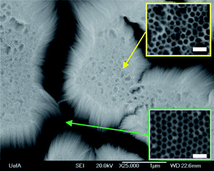 | ||
| Fig. 1 Top-view FESEM image of Ta2O5 nanotubes formed after 90 s of Ta anodization at 14.5 V (vs. Pt counter electrode) in 16.4 M H2SO4 + 2.9 M. Scale bars of higher magnification images shown in the insets are 100 nm in length. | ||
The lack of surface stability of the Ta oxide NTs at longer anodizing times in the 16.4 M H2SO4 + 2.9 M HF solution was explained by a model9 that predicted that the relatively fast migration of fluoride ions in compact Ta oxide films16,17 results in the build-up of a thin fluoride-rich (likely TaF5) layer at the Ta/Ta2O5 interface. The existence of this layer has been confirmed using time-of-flight secondary ion mass spectrometry (TOF–SIMS).18 As the TaF5 layer has a much higher ionic resistivity than does Ta oxide,19 the fraction of the applied voltage remaining to drive oxide anions across the Ta2O5 layer is lowered. This causes the compact Ta oxide layer to thin, in turn causing the overlying Ta oxide NTs to detach uncontrollably from the Ta surface. It is known that porous oxide formation occurs at metals such as Al20 only if the compact oxide layer is thicker than a threshold value. Similarly, in the case of longer times of Ta anodization, further Ta oxide NT growth cannot occur on top of the TaF5/Ta2O5 compact layer.
Based on this model, it was therefore hypothesized that a lower fluoride ion concentration (but maintaining a constant H2SO4 concentration) should decrease the extent of fluoride ion penetration into the compact oxide film, thus stabilizing the NTs, while still allowing sufficient Ta oxide dissolution to form a porous oxide layer. It was also postulated that this would allow the Ta oxide film to thicken to the point that stable, free-standing nanotubular Ta oxide membranes could then be formed.
(b) Formation of thick Ta oxide nanotubular films and free-standing membranes
To attempt to form substantially thicker Ta oxide NTs while also minimizing film cracking, the HF concentration was decreased from 3.0 to 0.5 M, while keeping the H2SO4 concentration fixed at 16.4 M. Fig. 2(a–c) shows the cross-sectional FESEM images obtained following Ta anodization (10 min at 14.5 V) in some of these lower concentration HF solutions. In contrast to the case in 2.9 M HF (Fig. 1), in which the nanotubular structures detach after ∼1.5 min of anodization, thus limiting their length to ∼2.7 μm, anodization in solutions containing lower HF concentration (Fig. 2) was found to give a stable and uniform layer of nanotubes of at least 8 μm in length.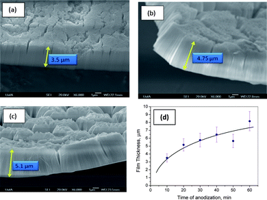 | ||
| Fig. 2 Cross-sectional FESEM views of Ta2O5 nanotubes formed after 10 min of Ta anodization at 14.5 V (vs. Pt counter electrode) in 16.4 M H2SO4 + (a) 0.51 M, (b) 0.85 M, and (c) 1.17 M HF, while (d) shows the FESEM-determined oxide film thickness as a function of anodization time of Ta in 16.4 M H2SO4 + 0.51 M HF. | ||
Although the films shown in Fig. 2 still contain some cracks, at least in the outer regions of the films, they do not have the undesirable, patchy morphology seen for films9 formed at higher HF concentrations (Fig. 1). Fig. 2 also shows that the full layer of NTs, formed at lower HF concentrations, remains well-attached to the Ta substrate. Further, these Ta oxide NTs (Fig. 2) are perpendicular to the substrate, do not show any sign of pore sealing, and contain pores of constant diameter (15–20 nm), even with changing HF concentration. These results clearly show that organic additives8 are not essential to the growth of long, stable Ta oxide NTs in HF/H2SO4 solutions. In addition, these data argue that the fluoride-rich layer (likely TaF5), formed at the Ta/Ta oxide interface, is indeed likely to be the cause of Ta oxide NT detachment. For this reason, the HF concentration should be kept sufficiently low to form mechanically stable, high-aspect-ratio Ta oxide NTs (Fig. 2).
An important new discovery made here is that, as hoped, Ta anodization in these lower concentration HF solutions can result in Ta2O5 nanotubular films that are easily removed from the Ta substrate in an intact form (with tweezers or using tape) without damage. Fig. 3 shows an example of one of these free-standing nanotubular Ta oxide membranes (∼15 μm thick), formed by anodizing Ta in 16.4 M H2SO4 + 0.85 M HF for 60 min at 14.5 V. While anodization of Ta in the same solution, but for shorter times, produced membranes that are thinner than 15 μm, these were found to be more difficult to remove. This likely reflects the fact that the underlying barrier film must be sufficiently enriched in fluoride ions so that the bond between the Ta substrate and the NTs becomes weakened. In fact, the lower the HF concentration, the longer the time required before the nanotubular oxide films can be detached from the Ta substrate as free-standing membranes.
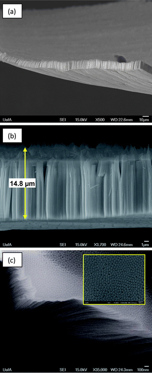 | ||
| Fig. 3 (a) Low magnification and (b) higher magnification FESEM images of free-standing nanotubular Ta oxide membrane, prepared by Ta anodization in 16.4 M H2SO4 + 0.85 M HF for 60 min at 14.5 V (vs. Pt counter electrode). (c) FESEM image of the base of the membrane, previously attached to Ta substrate. | ||
In contrast to some previous reports7,8 of porous and nanotubular Ta oxide formation, the films and membranes formed here in organic-free media are characterized by NTs that have a uniform thickness (Fig. 2 and 3), a non-patchy morphology (Fig. 2 and 3a), and that are hexagonally packed (Fig. 2 and 3c). This gives a very high surface area to volume ratio, which is of particular relevance for use as a dielectric material in electrolytic capacitors. Also unique here is that the free-standing membranes can be as large as several cm2 in area (Fig. 3a). The membranes, which consist of very well packed nanotubes, also show no sign of defects or cracks, they are thermally more stable and chemically more inert than composite organic–inorganic membranes, and they are mechanically superior to inorganic membranes, such as porous alumina. The membranes are easily transferable to other substrates, such as Si wafers or glass slides, making them potentially useful in sensor, optical, and catalysis applications.18
(c) Predicting Ta surface morphology from in situ electrochemistry
It was shown previously that Ta anodization in HF/H2SO4 solutions can result in a dimpled Ta surface,9–11 or, as shown here, in the formation of stable films or free-standing membranes, composed of long (up to 15 μm) Ta oxide nanotubes. These morphologies can be readily distinguished by ex situ FESEM analysis after anodization is complete. However, it would be of great interest to be able to determine the nanostructural morphology in situ, without the need for post factum microscopic analysis. This would serve to accelerate the identification of other combinations of metals and anodization conditions, leading to the formation of oxide NTs or dimpled surface morphologies, as desired.Here, we demonstrate how the current-time (i-t) data, collected at constant anodization voltage, can be used to easily and reliably determine the resulting surface morphology (dimples vs. attached nanotubes (or detachable membranes)) formed during anodization. Fig. 4 shows the i-t results obtained during Ta anodization at 14.5 V in 16.4 M H2SO4 plus varying amounts of HF. At all HF concentrations, the current initially (region A, in the first few seconds) decreases rapidly due to Ta oxide barrier film formation, similar to what has been reported previously at metals such as Al,21 in both neutral and acidic media.
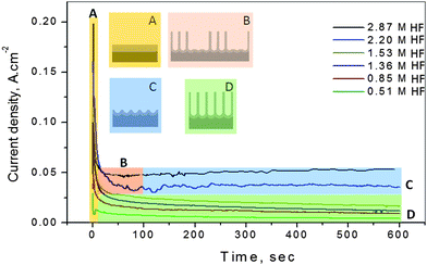 | ||
| Fig. 4 Current-time response during Ta anodization at 14.5 V vs. Pt in room temperature 16.4 M H2SO4 solutions containing the HF concentrations indicated in the figure. The rapid current decay in region A represents barrier oxide formation at all HF concentrations. In region B, at HF concentrations >2.2 M, only a patchy Ta oxide nanotubular film is formed, followed by its detachment in region C, exposing an ordered dimpled Ta surface. At HF concentrations <1.5 M, stable Ta oxide NTs lengthen with time throughout region D, resulting in a slowly decreasing current density. These Ta oxide films can be removed from the Ta substrate at various times in region D, producing free-standing nanotubular membranes with a thickness increasing with anodization time. | ||
At HF concentrations of 2.2 M or more, barrier oxide formation is followed by a period of time during which (region B) a patchy film of Ta oxide NTs up to ∼3 μm in thickness (Fig. 1) can be formed. The current then reaches a pseudo-steady-state after about 2 min (onset of region C), when the nanotubular film detaches from the surface and falls apart and a dimpled Ta surface (covered with a thin barrier oxide film) is then the stable morphology. These data indicate the time at which the nanotubes are detached from the surface (the inflection point at about 100 s between regions B and C), as confirmed by FESEM analysis.9 Under these conditions, the current would be expected to reach a steady-state due to the dynamic equilibrium between oxide growth and dissolution. However, it is seen that the current density increases very slowly with time in region C. This is attributed to an increase in the solution conductivity as the solution temperature increases (Joule heating) with time of passage of these relatively high anodization currents (∼50 mA). In fact, the solution temperature was found to have increased from 22.5 °C to 25.5 °C in 10 min, consistent with these predictions.
When Ta is anodized in HF concentrations less than ∼1.5 M, region A is followed by region D (Fig. 4), in which the current density decreases continuously with time of anodization. Based on Fig. 2, it can be seen that this is the same concentration range over which Ta oxide NTs are the stable surface structure produced. This continuous decrease in current likely reflects the development of transport limitations of the fluoride ion, protons, and water (reaction 2) into and out of the NTs as they lengthen.22 Indeed, there is no indication of the presence of a stable dimpled Ta surface morphology, using FESEM, at these lower (<1.5 M) HF concentrations. As long as the current is dropping, the NTs are still stable on the substrate surface and, when desired, they can be mechanically separated as membranes.
Overall, a continual decrease in current density with time (region D in Fig. 4), after the initial current decay, indicates stable nanotubular (or porous) Ta oxide formation. In contrast, a steady-state current or very slow increase in current density (region C, Fig. 4) indicates that the oxide nanotubes are unstable and that a dimpled Ta surface morphology is left behind when the nanotubes are lost from the surface. These findings therefore show that the i-t data can be used to accurately predict the Ta surface morphology. These results are extremely reproducible and may well contain more quantitative information about the surface properties, as well as the rate limiting steps of NT and dimple formation.
In order to determine how broadly applicable these in situ electrochemical predictions of the Ta surface morphology are, i-t data were collected during Ta anodization (at 14.5 V vs. the Pt counter electrode) in 16.4 M H2SO4 + 2.9 M HF + 10 wt% ethylene glycol (EG), another solution recently shown8 to form stable Ta oxide NTs. The chronoamperometry (i-t) data indeed do show a continuous decrease in the current density during anodization in this solution (Fig. 5, curve a), consistent with Ta oxide NT formation. In the absence of EG (Fig. 5, curve b), a steady-state current is seen (loss of NTs from the surface, with resulting dimple formation). These results confirm that the i-t data are extremely useful in the in situ prediction of the surface morphology of anodized Ta, regardless of the anodizing bath composition. This is very significant, as this approach will therefore be very useful for the rapid screening of other valve metals (Zr, W, Ti, etc.)/solution combinations in order to produce a desired surface morphology (dimples or NTs/membranes).
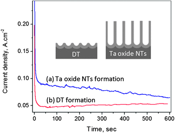 | ||
| Fig. 5 Current-time data during early times of Ta anodization in room temperature 16.4 M H2SO4 + 2.9 M HF solution in the (a) presence and (b) absence of 10 wt% ethylene glycol, all at 14.5 V vs. Pt counter electrode. | ||
Conclusions
Prior to this work, it was known that ordered Ta oxide nanotubes, up to ∼3 μm in thickness, could be fabricated by the anodization of Ta at 14.5 V (vs. a Pt CE) in 16.4 M H2SO4 + 2.9 M HF, a solution previously found to form only a highly ordered array of nano-scale dimples on the Ta surface. However, the Ta oxide NTs formed under these conditions suffer from a patchy morphology, and are also uncontrollably lost from the substrate when efforts are made to lengthen them further by anodization for longer than a few minutes. Work by others has shown that Ta oxide nanotubes can also be fabricated by anodization in acidic media containing organic additives. However, these nanotubular films are also quite patchy and have walls showing considerable thickness variations (ripples), which is not desirable.The detachment of these relatively thin nanotubular films in aqueous acidic media is attributed here to the use of high HF concentrations that results in the gradual build-up of a thin TaF5 film beneath the nanotubes. To test this prediction, the HF concentration was lowered and it was found that, at less than ∼1.7 M HF, films consisting of stable and adherent Ta oxide NTs up to 15 μm in thickness can be rapidly formed. It was also shown that these films can be removed from the Ta surface, under specific electrochemical conditions, producing intact, free-standing membranes that are characterized by a uniform thickness, a non-patchy morphology, and hexagonally packed NTs. These membranes are thermally more stable and chemically more inert than composite organic–inorganic membranes and mechanically superior to inorganic membranes, such as porous alumina. The membranes are easily transferable to other substrates, such as Si wafers or glass slides, making them potentially useful in sensors, optics, and catalysis and the thickness of the membranes can be controlled by tuning the HF concentration and the time of anodization.
We have also correlated the characteristics of the current-time data obtained during Ta anodization with the formation of either NTs (and membranes) or dimples. A continual decrease in current density with time indicates stable nanotubular (or porous) Ta oxide formation, while a steady-state or very slow increase in current density indicates that the NTs are no longer stable, resulting in the loss of the film into solution and resulting in a dimpled Ta surface morphology. The validity of this new in situ surface morphology determination method was confirmed for at least one other set of conditions. This provides a simple, in situ screening method that can be used to predict the surface morphology of other anodized valve metal surfaces (e.g. Zr, W, and Ti) formed using a range of anodizing conditions.
Experimental methods
Materials
H2SO4 (95–98%), acetone, and isopropanol (all ACS reagent grade) were purchased from EMD Chemicals, HF (48–51%, ACS reagent grade) and Ta foil (99.95%, 0.127 mm) from Alfa Aesar, and ethylene glycol (anhydrous, 99.8%) from Sigma Aldrich. All chemicals were used as received without any further purification, and all solutions were made up with deionized water (Corning Mega-Pure system).Electrochemical methods for Ta oxide nanotubular film/membrane and dimpled Ta fabrication
Ta specimens (10 mm × 5 mm) were cut from the as-received Ta foil and were carefully rinsed, sequentially, in acetone, 2-propanol, and deionized water. Anodization was then carried out using a Solartron 1287A potentiostat (or sometimes a Harrison 6824A power supply) for 5 s to 60 min at 14.5 V vs. the counter electrode (Pt gauze). A magnetically stirred, room temperature (∼23 °C) solution of concentrated H2SO4 (typically 16.4 M) containing different concentrations of HF (0.5–3 M) was employed in all of this work.When collecting the current-time data during anodization, the Pt counter electrode, placed at a distance of 1 cm from the Ta electrode, was also used as a reference electrode. No other reference electrodes were used due to the aggressive nature of the anodizing solution. Immediately after (within <5 s) anodization was complete, the samples were rinsed with copious amounts of deionized water and then dried using a hot air gun.
Surface characterization methods
Anodized Ta samples were mounted on Al stubs using double-sided carbon tape and/or Ag paint. Field emission scanning electron microscope (FESEM) analysis (Hitachi S-4880 FESEM, Alberta Centre for Surface Engineering and Science, Edmonton, Alberta) of the sample surfaces was then performed using an electron energy of 20 keV.Acknowledgements
The authors gratefully acknowledge the financial support of the Natural Sciences and Engineering Research Council of Canada for financial support of this work and the Alberta Ingenuity Fund for scholarship support of HAE. We also acknowledge the assistance of Drs Dimitre Karpuzov and Shihong Xu (Alberta Centre for Surface Engineering and Science, Edmonton, Alberta) with the FESEM studies, as well as E. El-Sawy, S. Gharaibah, and Dr F. Feng (all at the University of Calgary) for experimental assistance and useful discussions.References
- C. Chaneliere, J. L. Autran, R. A. B. Devine and B. Balland, Mater. Sci. Eng., R, 1998, 22(6), 269–322 CrossRef.
- I. Sieber, B. Kannan and P. Schmuki, Electrochem. Solid-State Lett., 2005, 8(3), J10–J12 CrossRef CAS.
- L. Young, Anodic Oxide Films, Academic Press, New York, 1961, p 377 Search PubMed.
- I. Sieber, H. Hildebrand, A. Friedrich and P. Schmuki, J. Electroceram., 2006, 16(1), 35–39 CrossRef CAS.
- I. V. Sieber and P. Schmuki, J. Electrochem. Soc., 2005, 152(9), C639–C644 CrossRef CAS.
- J. M. Macak, H. Tsuchiya, L. Taveira, S. Aldabergerova and P. Schmuki, Angew. Chem., Int. Ed., 2005, 44(45), 7463–7465 CrossRef CAS.
- W. Wei, J. M. Macak and P. Schmuki, Electrochem. Commun., 2008, 10(3), 428–432 CrossRef CAS.
- N. K. Allam, X. J. Feng and C. A. Grimes, Chem. Mater., 2008, 20(20), 6477–6481 CrossRef CAS.
- H. A. El-Sayed and V. I. Birss, Nano Lett., 2009, 9(4), 1350–1355 CrossRef CAS.
- H. El-Sayed, S. Singh, M. T. Greiner and P. Kruse, Nano Lett., 2006, 6(12), 2995 CrossRef CAS.
- H. El-Sayed, S. Singh and P. Kruse, J. Electrochem. Soc., 2007, 154(12), C728 CrossRef CAS.
- S. Singh, W. R. T. Barden and P. Kruse, ACS Nano, 2008, 2(12), 2453–2464 CrossRef CAS.
- J. E. Barton, C. L. Stender, P. Li and T. W. Odom, J. Mater. Chem., 2009, 19(28), 4896–4898 RSC.
- J. Wang and Z. Q. Lin, Chem. Mater., 2008, 20(4), 1257–1261 CrossRef CAS.
- J. Wang and Z. Q. Lin, J. Phys. Chem. C, 2009, 113(10), 4026–4030 CrossRef CAS.
- K. Shimizu, K. Kobayashi, G. E. Thompson, P. Skeldon and G. C. Wood, Philos. Mag. B, 1996, 73(3), 461 CrossRef CAS.
- K. Shimizu, K. Kobayashi, G. E. Thompson, P. Skeldon and G. C. Wood, J. Electrochem. Soc., 1997, 144(2), 418–423 CrossRef CAS.
- S. Singh, M. T. Greiner and P. Kruse, Nano Lett., 2007, 7(9), 2676–2683 CrossRef CAS.
- K. Shimizu, G. M. Brown, H. Habazaki, K. Kobayashi, P. Skeldon, G. E. Thompson and G. C. Wood, Corros. Sci., 1998, 40(6), 963–973 CrossRef CAS.
- A. Despic, V. P. Parkhutik, Electrochemistry of Aluminium in Aqueous Solutions and Physics of Its Anodic Oxide, Modern Aspects of Electrochemistry, Plenum Press, New York and London, 1989, vol. 20, ch. 6, pp. 401–503 Search PubMed.
- A. Eftekhari, Nanostructured Materials in Electrochemistry, Wiley-VCH, Germany, 2008, pp 6–10 Search PubMed.
- J. W. Diggle, T. C. Downie and C. W. Goulding, Chem. Rev., 1969, 69(3), 365 CrossRef CAS.
| This journal is © The Royal Society of Chemistry 2010 |