Effect of N/B doping on the electronic and field emission properties for carbon nanotubes, carbon nanocones, and graphene nanoribbons
Shan-Sheng
Yu
a and
Wei-Tao
Zheng
*b
aDepartment of Materials Science, Laboratory of Automobile Materials, MOE, Jilin University, QianWei Road 2699, Changchun, 130012, P. R. China. E-mail: yuss@jlu.edu.cn
bDepartment of Materials Science, State Key Laboratory of Superhard Materials and Laboratory of Automobile Materials, MOE, Jilin University, QianWei Road 2699, Changchun, 130012, P. R. China. E-mail: wtzheng@jlu.edu.cn; Fax: +86-431-85168246; Tel: +86-431-85168246
First published on 11th May 2010
Abstract
Carbon nanotubes, carbon nanocones, and graphene nanoribbons are carbon-based nanomaterials, and their electronic and field emission properties can be altered by either electron donors or electron acceptors. Among both donors and accepters, nitrogen and boron atoms are typical substitutional dopants for carbon materials. The contribution of this paper mainly provides a comprehensive overview of the theoretical topics. The effect of nitrogen/boron doping on the electronic and field emission properties for carbon nanotubes, carbon nanocones, and graphene nanoribbons is reviewed. It is also suggested that nitrogen is more an n-type donor. The discussion about the mechanism of field emission for N-doped carbon nanotubes and electronic structures of N-doped graphene nanoribbons is interesting and timely.
 Shan-Sheng Yu | Dr Shan-Sheng Yu born in 1974, is Associate Professor at the School of Materials Science and Engineering, Jilin University, P. R. of China. He obtained his Ph.D from Jilin University in the field of materials physics and chemistry in 2007. His research interests concentrate on nanomaterials including carbon related materials. |
 Wei-Tao Zheng | Dr Wei-Tao Zheng born in 1963, is Professor and Dean at the School of Materials Science and Engineering, Jilin University, P. R. of China. He obtained his Ph.D from Jilin University in the field of condensed matter physics in 1990, and visited the Department of Linkoping University, Sweden as a visiting scientist in 1997; Chiba Institute of Technology, Japan as a guest researcher in 1999; and Nanyang University of Technology, Singapore as a visiting professor in 2002. His research interests concentrate on thin film materials and nanomaterials including carbon related materials, as well as superhard materials. He has published 186 papers in peer-refereeing international journals. |
1. Introduction
Graphene is made up entirely of carbon atoms bound together in a network of repeating hexagons within a single plane just one atom thick, and exhibits fascinating properties arising from its hexagonal honeycomb lattice structures.1 In particular, graphene can be considered to be a basic unit for constructing other carbon materials including carbon nanotubes (CNT), carbon nanocones (CNC), and graphene nanoribbons (GNR). However, in order to tune their electronic structures and apply them to some special fields, the doping of elements such as nitrogen (N) or boron (B) atoms into these carbon nanomaterials are necessary.CNTs are nanostructures derived from rolled graphene planes, and have interesting quasi-one-dimensional character with honeycomb cylinders. The primary symmetry of classification of a CNT is based on either achiral or chiral. There are only two cases of achiral CNTs: armchair and zigzag CNTs, named by the shape of the cross-sectional ring of nanotubes. CNTs are uniquely characterized by their diameter and chirality.2 The armchair CNTs (n, n) are always metallic, while zigzag CNTs (n, 0) can be either semi-metallic, when n is a multiple of 3, or narrowband semiconductors, when n is not a multiple of 3. Since 1991,3 CNTs have drawn particular attention owing to their unique geometrical structures and novel physical properties. These unique properties make them promising candidates for building blocks of molecular-scale machines and nanoelectronic devices that may be synthesized using single-walled CNTs as a starting point.2,4–6
CNCs can be formed by introducing pentagonal defects into the honeycomb graphene layer, and those with a cone angle of 19°, 39°, 60°, 85°, and 113°, respectively, have been observed experimentally.7 In addition, the unusual type of cone-shaped structures, constructed by stacking CNCs with a constant cone angle or different cone angles, has also been synthesized.8,9 Due to their geometrical structures, CNCs are promising to be employed as practical phononic devices. For instance, they are ideally suitable for being scanning probe tips due to their small size and high stiffness in comparison with CNTs.10,11
GNRs can be viewed as strips cut from an infinite graphene sheet, and can be either patterned by plasma etching,12,13 derived chemically,14 or obtained by using a template method.15 In comparison with CNTs, GNRs also have only two symmorphic nanoribbons: armchair and zigzag GNRs, which, however, are named by the edge shape. For the other non-symmorphic nanoribbons, the edge shapes are irregular and complicated, which are ascribed to a mixture of armchair and zigzag sites.16 The electronic properties of GNRs are determined by the width and atomic geometry along the edge.17 Similar to armchair CNTs, GNRs with zigzag edges (ZGNR) are all metallic,16–18 while for GNRs with armchair edges (AGNR), the band-gap oscillations have been presented as a function of their widths.19–23 There is a very large density of states at the Fermi level in ZGNR, which is attributed to the edge with localized states having non-bonding character.24 The unpaired edge electrons give rise to a magnetic ordering in the system.19,25–27 Unlike CNTs, the existence of electron spin and half-metallic state in ZGNRs has led to several possible spintronic devices.28–31 Hence, there has been growing interest in GNRs as possible passive and active components in carbon-based nanoelectronics. In addition, the planar geometry of the ribbons allows for the application of standard lithographic techniques for the flexible design of a variety of experimental devices.32
The application of “graphitic” materials to nanoelectronic devices is based on their electrical properties, which strongly depend on their microscopic electronic structures. The doping of other elements into “graphitic” materials is the best way to control the electronic structures. It is well known that N and B atoms are ideal dopants within the lattice of carbon-based materials, as they have roughly the same atomic radius as carbon and can be easily incorporated into the carbon network through many different techniques. These dopants can inject electrons or holes, thus changing the electronic and transport properties for carbon-based materials. The n-doped or p-doped transistors can be produced by N/B doping, which are crucial for building logic functions and complex circuits.33–51 Furthermore, N/B doping has received particular attention, as N/B impurities can also give rise to functionalizing carbon nanostructures. These functionalized carbon materials can be applied as chemical sensors,52–54 field emitters,55–62 hydrogen storage63,64 or anode materials.65–67 Various techniques have been employed to incorporate N or B atoms into carbon materials, including chemical vapor deposition,68–71 magnetron sputtering,72–74 electric arc discharge,75–77 pyrolytic routes,78–80 and substitution reactions,81 in which the diverse bonding structures, such as pyridine-like, graphite-like, triple-bonded CN, molecular N2, and BC3 structures, of N/B atoms have been found.76,82–85 Alternatively, an atom-by-atom substitution technique using a scanning tunnelling microscope can also be realized to control nanostructures accurately.86 This review will discuss the doping of N or B atoms into CNTs, CNCs, and GNRs, and in particular, focus on the doping effect on their electronic and field emission properties.
2. Carbon nanotubes
2.1 Geometric structures
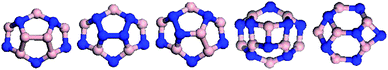
N/B atoms can be incorporated into the hexagonal network of CNTs through substituting carbon atoms, whose distributions also depend on the chirality and diameter of CNTs. When zigzag CNTs contain one substitutional N/B atom, the formation energies as a function of diameter can exhibit a periodic feature,43,47,50,87 which is also similar to that found in zigzag CNTs with adsorbed atoms,88 5-77-5 defects,89 and interstice,90 as well as the evolution of band gaps in perfect zigzag CNTs.91,92 These result from the different π bonding structures of the perfect zigzag CNTs with different diameters, rather than the defects in the tubes.43,87When CNTs are doped with two N/B atoms, the two doped atoms might be very near or far from each other. For the former case, two dopants lie in the same hexagon, in which two doped atoms are one, two and three bonds apart. In fact, the configurations containing two adjacent substitutional N/B atoms are energetically unfavorable because the N–N/B–B bonding is weaker than the C–C bonding, and the cases in which the distance between two doped atoms is three bonds apart are preferred in comparison with other isomers.41,43,50,93 However, for thin CNTs, it is found that some configurations containing two adjacent substitutional N atoms, as shown in Fig. 1, are also energetically favorable.42,93 The seamless cylindrical graphitic structure of CNTs yields a high Young's modulus which has been revealed theoretically and experimentally.94–97 The Young's modulus decreases with increasing tube diameter and approaches the modulus of a graphene sheet in the limiting case. It has been proved that this mechanical property also plays an important role in the distribution of N atoms in N-containing CNTs with a small diameter.93 For thin tubes, the C–C bond, which has very small angles with tube longitude, bears the high radial stress. When this C–C bond is replaced by N–N, the strong radial stress will break the N–N bond. Consequently, for the thin N-doped CNTs, the major contribution to the stabilization comes from the radial stress release after breaking the N–N bond. It is obvious that, for zigzag and armchair CNTs, the bonds could be classified into two types owing to their high symmetry, in which the smallest angle between bond and tube longitude is 60° and 0°, respectively. Therefore, for thin N-doped armchair CNTs, the radial stress is more easily subject to breaking chemical bonds between two nitrogen atoms along the circumference than the bonds for other kinds of CNTs.
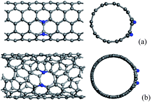 | ||
| Fig. 1 (a) (5, 5) and (b) (7, 4) carbon tubes containing broken N–N bonds, in which N atoms are labelled by blue balls. | ||
When more N/B atoms are introduced into CNTs, the pyridine-like structures appear popular in the N substitution case,38 while BC3 nanodomains are always formed in the B substitution case, which have been revealed theoretically and experimentally.76,83,98,99 For BC3 CNTs, there are two kinds of configurations, as shown in Fig. 2, in which the case in Fig. 2(b) is more stable than the isomer in Fig. 2(a). The strain energies of BC3 CNTs are smaller than those of the CNTs.98 Therefore, BC3 CNTs are energetically favorable. Under rich doped N atoms, for thin CNTs, the N atoms prefer to be localized, rather than distribute uniformly in Fig. 3, especially for armchair tubes.42,93 This suggests that the thin CNTs are more easily subject to opening of the tubular sheets than the thick CNTs. Therefore, the population of the thin N-doped CNTs will be small when the CNTs are synthesized under the existence of a nitrogen source. As the overall N content increases, the number of graphitic walls within the CNTs decreases, but the proportion of pyridine-like N (two-bonded N) increases. These pyridine-like N “cavities” or “edges” within the predominantly graphitic framework should be responsible for the interlinked morphologies observed in the N-doped CNTs.100
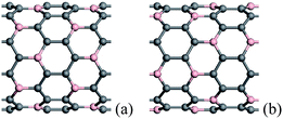 | ||
| Fig. 2 Schematic description of the two kinds of BC3 (10, 0) CNTs, in which the B atoms are denoted by pink balls. For each B atom, there are only two B atoms three bonds apart from it in configuration (a), and there are only three B atoms three bonds apart from it in configuration (b). | ||
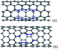 | ||
| Fig. 3 The configurations containing six substitutional N atoms after geometry optimization, in which the N atoms align in two rows parallel to the tube axis, (a) and (b) corresponding to (5, 5) and (10, 0) CNTs. The N atoms are denoted by blue balls. | ||
2.2 Electronic properties
For the low concentration of N/B dopants, the dopants are uniformly distributed in the CNT, and the impurity states introduced by dopants will appear in the band gap, which are regarded as donor states for N doping and acceptor states in the case of B. The impurity states are localized near the N/B atoms, which are induced by the extra electrons of N dopant or the missing electrons (hole charge) of B dopant. The donor state is close to the conduction band minimum (CBM), while the acceptor state appears near the valence band maximum (VBM), as shown in Fig. 4. In addition, the localization of the extra charge associated with the isolated impurity shows a striking difference between the metallic and semiconducting CNTs. Compared with a metallic tube, for a semiconducting tube, the defect state in the band gap is spatially more localized.40 Hence, the N-doped semiconducting tube is quite different from the metallic tube in chemical and electrical properties.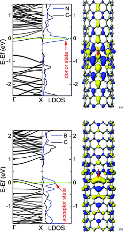 | ||
| Fig. 4 Electronic structures for (10, 0) CNTs containing N (a) or B (b) dopants. The middle panel is the local density of states (LDOS), in which N or B dopants and its two nearest-neighbor C atoms are labelled by the blue line, and the three C atoms far away from the dopant are labelled by the dark line, and the impurity states are marked by arrows. The right panel is the qualitative descriptions of impurity states. The sites of N and B dopants are marked by arrows. The isosurface value is ±0.017 electrons au−3. The concentration of dopant is about 0.36%. | ||
For N-doped CNTs, the n-type behavior should not be immediately inferred.101 The structure means that a p-type doping may also be achieved, and the electronic behavior depends on the arrangement. When the two N dopants occupy in the same hexagon, they will prefer to lie three bonds apart in Fig. 5(a) and (b).43 Due to the interaction between two extra electrons, their impurity states shift towards the valence band in comparison with the configuration where the two dopants are far away each other, as shown in Fig. 5(c), especially in comparison with the symmetric configuration along the tube axis, as shown in Fig. 5(a). This means that the extra electrons need much more energy to be excited from the impurity level to the conduction band. However, for the CNTs with a very small diameter, the two N dopants tend to be adjacent to each other along the circumference. For example, for (5, 5), (6, 6) and (7, 4) tubes, the N–N bond is broken due to radial stress, as shown in Fig. 1, and then a ten-membered ring (10 π system) is formed. Their impurity states will shift downwards, and appear below the Fermi level owing to N non-bonding lone-pair states,42,93 as shown in Fig. 5(d). Likewise, for other CNTs containing twofold-coordinated N atoms, such as pyridine-like structures42 and N adatoms,102 the impurity states are also much pronounced and localized near the VBM, as shown in Fig. 5(e) and (f). In addition, if the CNTs are semiconducting, these N dopants will act as p-type doped CNTs. This suggests that the N atom is more beyond n-type donor owing to possible reactions, and the electronic properties of CNTs can be controlled by adjusting the N doping manner.
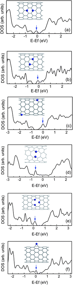 | ||
| Fig. 5 The density of states (DOS) for (10, 0) CNTs containing two N dopants (a–c), (7, 4) CNTs doped with two adjacent N atoms (d), and (10, 0) CNT with pyridine-like structure (e), or N adatom (f). The impurity states are marked by arrows. | ||
For the high concentration of N dopants, the CNx tubes can be transferred from semiconducting to metallic, in which N atoms are predominantly divalent and form pyridine-like structures.37–39 However, for the high concentration of B dopants, the formation of BC3 nanodomains is preferred theoretically and experimentally, as shown in Fig. 2, and their band structures are exhibited in Fig. 6. For the case in Fig. 6(b), there are dispersive unoccupied acceptor bands within the band gap, which derive from the carbon levels hybridized with the acceptor levels owing to the strong concentration of B atoms.50 However, for another case in Fig. 6(c), it exhibits a band gap between occupied and unoccupied π orbitals, resulting in the semiconducting behavior, compared to the metallic case, as shown in Fig. 6(b). In addition, it is also noted that there is a small band gap, marked by an arrow between two conduction bands, viz., between π and π* bands, at the Γ point above the Fermi level. This gap shows an oscillation with the tube diameter, which corresponds to the band gap oscillation found in the perfect zigzag CNTs.98
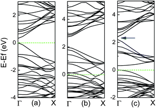 | ||
| Fig. 6 Band structures for (10, 0) CNTs per two units with (a) perfect, (b) BC3 configuration in Fig. 2(a), and (c) BC3 case in Fig. 2(b), in which Fermi level is labelled by dashed line. A band gap in the conduction bands is marked by an arrow. | ||
The N/B dopants can also induce a strong asymmetric damping of the electronic conductance, and N (B) doped CNTs exhibit a negative (positive) derivative with respect to the energy at the Fermi level. Due to localized states introduced by N/B atoms, the backscattering for energies near the charge neutrality point is enhanced. For a low density of dopants, mean-free paths decrease linearly with increasing dopant concentration, but increase linearly with increasing tube diameter.103 In addition, for individual N-doped CNTs, the n-type conduction can be only achieved by graphite-like N bonding configuration, while the pyridine-like structure can mainly lead to the electric-dipole scattering.104
2.3 Field emission properties
The intrinsic mechanism of the field emission for CNTs is different from that of the conventional metallic tips, and is more complicated. As for the quasi-one-dimensional structure CNT, the field emission process can be described as follows: the valence electrons localized at discrete energy levels are emitted from the CNT tip and pass through the potential barrier to the vacuum under the applied electric field. The field emission properties can be characterized by the work function, ionization potential (IP), and tunnelling probability. The work function is a critical quantity in understanding the field emission properties of material, defined as the minimum energy required for one electron to be removed from the material to the vacuum, which is related to the turn-on voltage in the field emission experiments. Several investigators have attempted to estimate the work function of CNTs by using experimental measurements,105–107 confirming that CNT is a good field emission material owing to its unique quasi-one-dimensional geometrical characteristics. Without the electric field, both the highest occupied molecular orbital (HOMO) and the lowest unoccupied molecular orbital (LUMO) of a perfect CNT are the extended states in the body. Furthermore, under the applied electric field, the energy of LUMO + 1 localized on the tip will decrease as compared to that of HOMO and LUMO in the body.60,108 Hence, the electrons are easily emitted from the CNT tip under the electric field. However, in order to enhance the field emission properties of the CNT, the elevation of the Fermi level can be considered, in which the doping of CNT is an effective way. The actual emission current for the doped CNT depends strongly on the doping configuration, which is related to either the doping element or the doping position. For the N doped case, the body-cap joint of CNT is the preferable doping site,60 while for the B doped case, the tip of CNT is the favorable doping site,109 as shown in Fig. 7.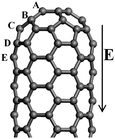 | ||
| Fig. 7 The geometrical structure of (5, 5) CNT. For the N doped case, the most preferable doping position appears at the fourth layer D, which is the link between the cap and the body of CNT. For the B doped case, the first layer A, viz., tip, is favourable doping site. | ||
For CNTs, when the C atom is substituted by the N atom, the work function and the first IP will decrease drastically, which has been revealed theoretically and experimentally.58,60,110 The reduction in the work function and IP means an enhancement in the field emission properties of CNT. On the contrary, the B-doped CNTs result in a higher work function and IP than perfect CNT, under the applied electric field.61,109,111 This implies that the B doping will impede the field emission of CNT. The tunneling probabilities for the N doped CNT increase after N doping, while those for the B doped CNT decrease after B doping, compared to perfect CNT, as shown in Fig. 8. After N/B doping, the change in work function, IP, and tunneling probability shows a similar trend. When N atoms are incorporated into CNTs, the Fermi level will be shifted upwards due to the extra electrons from the N atom, while for the B doped case, the Fermi level will be shifted downwards. Furthermore, the coupled states will be introduced by N dopant, which mix both the localized states and the extended states. When the electric field is applied, the coupled states will be filled with electrons transferring from other states, and then the electrons will be leaked out completely.60,108 Accordingly, the N dopant will lower the potential barrier of the electron emission for the CNT tip, and increase the probability of an electron escape from the surface of CNT to the vacuum. In contrast, the B dopant will make the field emission difficult due to the electron holes from the B atom. In comparison with the theoretical predictions, experimental results have also confirmed that N-doped CNTs showed a lower turn-on field and a higher emission current density than those of the undoped CNTs.112 The N-doped CNTs indicated the considerably good field emission stability even though they showed decreased crystallinity owing to pyridine-like N structures. The work function of the N-doped CNT is also sensitive to the temperature and shows a lower value at lower temperature,58 which may be attributed to the impurity molecules adsorbed on the cap of CNT, such as water molecules which can locally enhance the emission.113–116
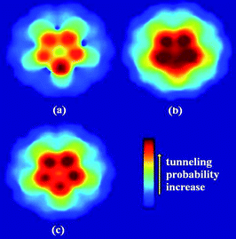 | ||
| Fig. 8 Tunneling probability patterns for HOMO of (a) first-layer B-doped, (b) first-layer N-doped, and (c) perfect CNTs under the applied electric field of 0.5 V/Å. Arrow in the color map denotes an increase of the tunneling probability. | ||
According to orbital distribution, there are three types of orbitals contributing to the emission current of CNT.108 As shown in Fig. 9, the first one is the extend orbitals located near the Fermi level and distributed in the body (T1). The second one is the localized orbitals located near the Fermi level and distributed at the tip (T2). The third one is the localized orbitals located deeply below the Fermi level and distributed at the tip (T3). For the N-doped CNT, the coupled states mainly locate around the N atom and should be considered as T2 orbitals, which play an important role in the emission properties of the N-doped CNTs. The emission currents from these three types of orbitals can be calculated. Under a low electric field, the total emission currents increase drastically for the N-doped CNT in comparison with the perfect CNT, which is mainly contributed by the couped orbitals (T2), while the currents form T1 and T3 orbitals change slightly, as shown in Fig. 10. The coupled orbital is localized, having a higher electronic density at the tip and larger emission area, as compared to T1 orbitals. These features lead to the current from the coupled orbital being much larger than that from the other orbitals, and play a dominant role in the total current under a lower electric field.
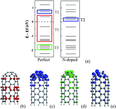 | ||
| Fig. 9 (a) Schematic energy levels for the perfect and N-doped CNTs. Side view of three typical orbitals in the perfect CNT are exhibited in (b), (c) and (d) which correspond to T1, T2 and T3 orbitals. The T2 orbital of the N-doped CNT is plotted in (e). | ||
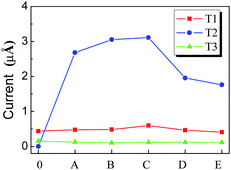 | ||
| Fig. 10 The emission currents of (5, 5) CNT from different types of orbitals, in which the capital letters denote the doping layer of CNT in Fig. 7, and 0 denotes the perfect CNT. | ||
However, under a high electric field, although the emission current of the N-doped CNTs also increases in comparison with that of the perfect CNTs, the increase in the total current from T2 orbitals is less pronounced than that under a lower electric field.108 Under a strong applied electric field, the structure–vacuum barrier height decreases at very short distances near the nanotube surface. In addition, T3 orbitals show larger electronic densities at the emission side, viz., at the CNT tip, and are substantially exposed to the electric field, which results in larger emission areas. Consequently, the tunneling probability of the electronic states located deeply below the Fermi level increases, resulting in a large contribution of deep electronic states to the total current.
3. Carbon nanocones
CNCs have various geometry structures, in which the nanocone with a larger cone angle is energetically favorable, as a result of the low strain energy arising from small curvature. Energy minimization leads to 60° disclination structures with an isolated pentagon at the tip, as shown in Fig. 11.117 The individual CNC can exhibit good emission properties, having a low emission threshold, high carrier current densities, and a long emission lifetime.118 This originates from the pentagonal ring of carbon atoms in the cone tip where there is high local density of states near the Fermi level, and these states are well localized.119–122 The work function and electron density for CNC do not depend critically on the cone angle, but the position and the number of pentagons. The CNC with three pentagons has the large field emission current.122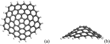 | ||
| Fig. 11 The geometrical structure of CNC, (a) the formation of a CNC from a graphene sheet with a 60° disclination, (b) the lateral view of the proposed CNC. | ||
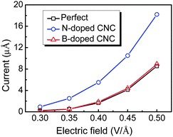
In order to achieve a large DOS near Fermi level on the emission site, the doping sites on the top of CNC are considered. The field emission properties of the doped CNC depend on the doping species, site, and concentration. The N atom is more easily introduced into the CNC, in comparison with the B atom, and the B doped atom can produce stronger distortions than the N doped atom.62 As shown in Fig. 12, the emission currents for the perfect and doped CNCs with one N/B atom vary with the applied electric fields from 0.3 to 0.5 V/Å. Similar to CNT, N dopant can upshift the Fermi level in the CNC, and hence reduces the work function and increases the emission current.62 Thus, the electron emission for CNC is enhanced after N doping. In contrast, B doping has no significant effect on the field emission properties of CNC.
 | ||
| Fig. 12 Calculated emission currents versus the electric field for CNC. | ||
When CNC is doped with two foreign atoms on the top, the doping concentration will be twice as that containing one foreign atom. For the N doped case, especially for two N dopants on the pentagon ring, the emission current is increased significantly, in comparison with the case containing one N atom. However, for the B doped case, there are no significant changes in emission current, compared to that doped with one B atom. In addition, when the two N dopants are adjacent to each other on the pentagon ring, it is worth noting that the properties of field emission are enhanced more drastically than other configurations with two N-doped atoms being apart.62 This is because that N–N bond on the pentagon ring can induce more localized electronic states at the apex, and hence the tunneling probability is enhanced.
As a promising cold field emitter, boron nitride nanocone (BNNC) is another interesting nanomaterial. It has been demonstrated both experimentally and theoretically that the topology and materials component for BNNC are two important factors to affect electron emission.123–126 BNNC includes pentagonal defects and other topological defects at their tips, which consists of three types of covalent bonds, that is B–B, N–N and B–N bonds, as shown in Fig. 13. The homonuclear bonds can affect the physical, chemical and electronic properties for BNNC. The type of chemical bond for BNNC is more important than the specific topology in governing the electron field emission.126 Under the applied electric field, either N–N or B–B homonuclear bonds at the tip can induce several orbitals near the Fermi level, and result in the highest tunneling probability for occupied orbitals. Therefore, the nanocones with homonuclear bonds at the tip can increase the emission current. Moreover, the N–N bond increases emission current more significantly than B–B bond.
 | ||
| Fig. 13 Top views of BNNCs with 240° disclination angle, in which the B and N atoms are colored in pink and blue. | ||
4. Graphene nanoribbons
The structures of GNRs are similar to CNTs which can be unwrapped into GNRs. However, in contrast to CNTs, GNRs do not always present a well-defined parity associated to mirror reflection with respect to their axis. Due to edge confinement, their electronic properties are different from those of CNTs. For carbon-based nanomaterials, the edge trapping of the bonding electrons and π-electron polarization play a significant role because they can modify the density of states and band gap.127 In addition, the chemical edge modifications can also affect the electronic properties of GNRs.128,129 In order to explore the intrinsic properties of GNR, the edges are generally passivated with hydrogen atoms.4.1 ZGNR
The DOS at Fermi-level and electron correlation are two major factors that induce the ferromagnetic ordering in itinerant electron systems.25 For ZGNRs, the electron states localized near the edge, called edge states, are located at the Fermi level in energy, which result from a delicate balance of electron transfers among π orbitals situated near edge atom. Hence, the unpaired π/π* edge electrons will lead to magnetic properties, which have been examined by various theoretical and computational simulated methods.19,25–27,130,131 There are three magnetic phases, as shown in Fig. 14: the antiferromagnetic (AFM) phase with the opposite spin direction between the edges, which is the most stable; the ferromagnetic (FM) phase in which the spins are in the same direction at both edges; and then the non-magnetic (NM) phase, which is explained by an enhanced exchange splitting between spin-up and spin-down π-orbital states.26 However, the difference between AFM and FM phase is slight, and transition between them can be realized easily. Besides depending on magnetic ordering, the transport behaviors under bias voltages are also related to the symmetry between two edges.132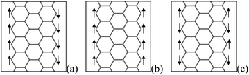 | ||
| Fig. 14 Structure of the electronic spin of an isolated ZGNR with an open edge, and (a), (b) and (c) correspond to the AFM, FM and NM spin configurations, respectively. | ||
ZGNRs have the peculiar localized unpaired π/π* edge electronic states which are extended along the edge direction. N/B doping can greatly modify the electronic structures, in particular, the edge states, and break the polarized transport degeneracy.31,129,133 These modifications depend on the doping sites, doping concentration, and nanoribbon width. As shown in Fig. 15(a), if one N dopant lies at the edge, the impurity states are below the Fermi level, while for one N dopant in the inner of the ribbon, the impurity states are above the Fermi level. When the isolated substitutional N (B) atom appears in ZGNR, an extra non-bonding electron (hole) introduced by N (B) will be affected by two factors.134 One is its Coulomb interaction with N+ (B−), and another is its correlation with charges at the edges. Thus, the site of impurity energy level is related to the competition between these two factors. When N (B) dopant lies at the edge, the impurity level locates below (above) the Fermi level owing to the strong Coulomb interaction, as shown in Fig. 15(b) and (c). In order to achieve the stable state, the π (π*) edge electron will be coupled with this non-bonding electron, and then the intensity of occupied (unoccupied) edge states near the Fermi level will decrease slightly. However, when the N (B) dopant locates far away from the edges, the correlation between unpaired π (π*) edge electrons and the extra electron (hole) is dominant, compared to the Coulomb attraction between the extra electron (hole) and N+ (B−), which means that this extra electron (hole) tends to appear at the edges and occupy the lowest (highest) unpaired π* (π) edge electron level, which shifts upward (downward) the Fermi level. The remained isolated N+ (B−) has a strong ability to attract negative electrons (positive holes), which can introduce the impurity level above (below) the Fermi level.
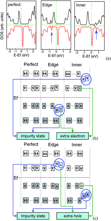 | ||
| Fig. 15 (a) DOS for perfect and N-doped 7-ZGNR per seven units, in which the impurity states are marked by arrows. Schematic diagram of impurity states induced by N (b) or B (c) at the edge and inner of ZGNR, in which occupied states are denoted by filled rectangles, the impurity states are presented by blue circles, the green arrows in the rectangles denote extra charge introduced by N/B atom, and Ef is the Fermi energy of perfect ZGNR. | ||
Due to strong edge states, the substitutional N/B atoms energetically prefer to be at the edge of ZGNRs.44,45,134 As the N/B doping concentration near the edge increases, the band gap will increase until it reaches the maximum, and then decreases.44 This can be explained that upon increasing the doping concentration, the number of edge states near the Fermi level decreases since the edge states are coupled with charges induced by N/B, resulting in those coupled states appearing. These coupled states will be away from the Fermi level, and thus open an energy gap. However, the number of edge states is limited, and cannot keep increasing if the doping concentration is too large. This means that the energy gap has a maximum value with an increase in the doping concentration. As more unpaired extra charges are further induced by N/B atoms, the energy gap will decrease gradually. Consequently, the energy gaps of ZGNRs can be tuned by N/B doping concentration at the edge, and thus ZGNRs can be changed from metallic to semiconducting. In addition, it is worth noting that the band gap of the ZGNR doped with N/B atoms is also influenced by the ribbon width. As the ribbon width increase, the band gap for the doped ZGNR decreases monotonically.44
The B and N doping at the edges of ZGNRs can further result in distinct charge transport properties for each spin channel.31,133 One spin channel will be scattered in a more confined energy range than another spin channel, and then the former will present higher transmittance at energies close to the Fermi level, as shown in Fig. 16. Like the energy gap, the stability of spin state and magnetic moments are also dependent on the concentration of the edge dopant.135 Hence, the spin polarization can be suppressed by the edge impurity.
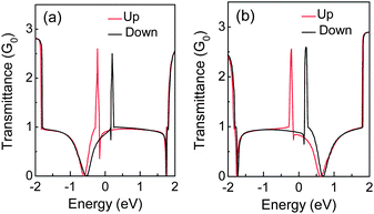 | ||
| Fig. 16 Transmittance of (a) N and (b) B-doped 4-ZGNR, in which the red (black) solid line is for spin up (down) channel. | ||
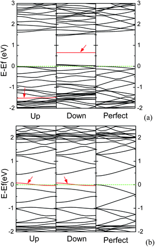
Half-metallic materials show metallic behaviour for one spin orientation, and show semiconducting or insulating behaviour for the other. It is observed that the half-metallicity emerges when a finite external electric field is applied across the AFM ZGNRs,19,136 which originates from the fact that the applied electric fields induce energy level shifts of opposite signs for the spatially separated spin ordered edge states. However, as the edge passivation of ZGNR is replaced with B atoms, the ground state will be FM due to large hole doping. The ZGNRs with B edges also show half-metallic behavior irrespective of the ribbon width even in the absence of electric field, and this property sustains for any field strength, since the spin polarizations of the opposite edges are the same.137 The half-metallic at Fermi energy in ZGNRs with B edges is largely contributed by the B orbitals at the edge. However, for the N doping case, ZGNRs show an AFM ground state and metallic behavior for both of the spins at Fermi energy. On the contrary, it is well known that the pyridine-like structure usually exists in the graphene-based systems. As the pyridine-like defect is incorporated into ZGNR, the degeneracy of spin polarization of the perfect ZGNR is broken, leading to the ZGNR becoming half-metallic.138
The edge states of ZGNR decay exponentially as the considered position moves from the edge to the centre of the ribbon,16,136 whose decay rates are related to the momentum for ZGNR. The edge state is very important as the ribbon width is at nanoscale. This is because the edge state for the narrow ribbon significantly influences the electronic properties for ZGNR. However, for the wider ZGNR, the doping at the edge will have no significant impact on the electronic properties such as the conduction efficiency,139 compared to the narrow ZGNR.
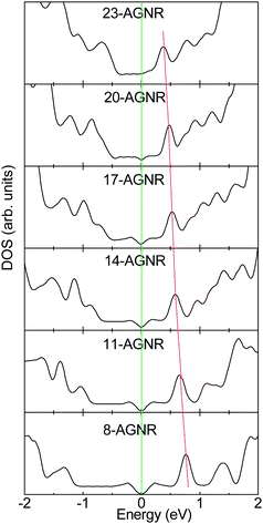
4.2 AGNR
Similar to zigzag CNTs, for AGNRs, the change of the band gaps with ribbon width exhibits a sawtooth-like shape. The DOS for AGNRs are not symmetric and that small splittings of some peaks emerge owing to the ribbon relaxation and width.23 However, AGNRs have edge states owing to the existence of edges, and the edge effect becomes significant with decreasing ribbon width.23,140 Likewise, unlike ZGNR, AGNR has a diamagnetic susceptibility since it has a zero density of states at the Fermi level.19,24The localized GNR edge states come from the polarization of the unpaired non-bonding states induced by the densely and deeply trapped σ-bonding electrons.141,142 For the ideal ZGNR, the edge states are apparent due to the deeper potential at the edge, whereas the edge states of AGNR are not prominent due to the inhomogeneous stress along the edge.For AGNRs, the substitutional N atom prefers to be at the edge since the density of π electrons at the edge is denser than that in the inner. In contrast, for the B doping case, the second row near the edge are the energetically favorable sites owing to the severe local structural distortion induced by the edge doped with B.51 As one isolated N/B atom is incorporated into a semiconducting AGNR, the Fermi level is shifted upwards/downwards due to the extra/missing π electrons from the N/B atom, and then AGNR is transformed from intrinsic semiconductor to n-type/p-type semiconductor, which are similar to those of semiconducting CNTs. However, the electronic structures for N/B-doped AGNR are different from those of N/B-doped CNTs.51 For the N-doped CNT, there is one striking impurity band falling below the CBM. The impurity band, called donor level, is mainly contributed by the excess electron which is localized near the N impurity site. As for the N-doped AGNR, the impurity band appears above the CBM, in which the excess electron has been transferred from the impurity band to the conduction band. The donor level is not an impurity band, which mainly comes from the lowest unoccupied level of perfect AGNR, as shown in Fig. 17(b). For the B-doped AGNR, the electronic structures are quite different from those of the N-doped AGNR, in which the impurity band is fully occupied, lying in the valence band. The acceptor level near the VBM is derived mainly from the highest occupied level of perfect AGNR, as shown in Fig. 17(c). The electronic states associated with the impurity band are distributed around the N/B substitutional site. As shown in Fig. 17, it is clear that the electronic states induced by impurity are unoccupied or occupied electronic states which come from π* antibonding or π bonding states of 2pz orbitals along the N–C or B–C bonds.51,64,143
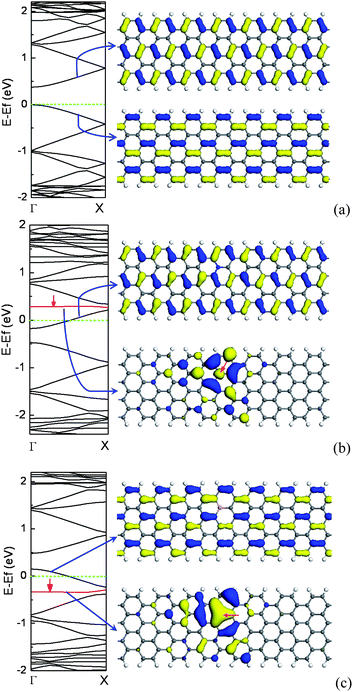 | ||
| Fig. 17 The electronic structure for a perfect 8-AGNR (a), containing one N dopant (b), and one B dopant (c) per seven units, and left are band structures, in which the impurity levels are denoted by the red line. For a perfect AGNR, the top right corner is an isosurface plot of LUMO and the bottom right corner is HOMO. For doped AGNR, the top right corner is an isosurface plot of donor (b)/acceptor (c) levels, and the bottom right corner is isosurface plot of impurity levels.The isosurface value is ±0.02 electrons au−3. | ||
It is the edge trapping of the bonding electrons and π-electron polarization effects that drive the impurity levels induced by N or B atoms to be autoionized so that the relevant charge carries can occupy the conduction or valence bands, which is independent of the doping site.51 As the N (B) doped AGNR is bent along the lateral direction, as shown in Fig. 18, the impurity band still appears above (below) the CBM (VBM). However, for the infinite two-dimensional system, even though a planar sheet of graphene is doped with N/B atom within a unit cell, the location of the impurity level is also similar to that of the doped CNT, owing to that the edge does not exist. Hence, the ionization of the impurity band is also not relevant to the curvature, viz., π hybridization.
 | ||
| Fig. 18 The electronic structures for the bended N-doped 8-AGNR per seven units, in which the impurity levels are marked by arrows. Fermi level is labelled by the dashed line, and the occupied states are filled by gray. | ||
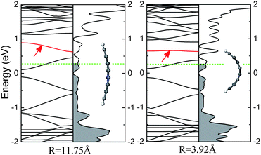
The unpaired non-bonding π electrons can be polarized by the nearby σ-bonding electrons.142 Due to the existence of the edge, the extent of polarization near the edge is larger than that in the interior of AGNR by the trapped bonding states. In contrast, for the CNT, the extent of polarization is homogenous owing to that the edge does not exist. As the C atom is substituted by N/B atom for AGNR, the excess non-bonding charge will be ionized owing to the inhomogeneous polarization and pinning of the unpaired non-bonding π electron by bond contraction, whereas the polarization of unpaired non-bonding π electron for CNT is homogeneous.51 With increasing the ribbon width, the unpaired polarized non-bonding π electron for AGNR becomes homogeneous. Correspondingly, the extent of the ionizing impurity atom by the edge polarization for the doped AGNR will decrease with an increase in homogeneity.23 Hence, the impurity state for the N (B) doped AGNR will be approaching the CBM (VBM) with increasing ribbon width, as shown in Fig. 19. In addition, for pyridine-like structures, they also prefer to lie near the edge in AGNRs.129 However, the impurity levels induced by the pyridine-like defects are below the VBM owing to the N lone-pair states, which are similar to those of CNTs.
 | ||
| Fig. 19 The impurity states for N-doped AGNRs per five units with the width dependence. The site of impurity state approaches the CBM when the AGNR width becomes larger. | ||
Being similar to the AGNR with substitutional N atom, for the AGNR containing adsorbed N atom, the electronic structures are also affected by the edge states, and the edges are the energetically favorable adsorbed sites.144 However, the electronic structures for the AGNR containing N adatom are different from those for the AGNR with substitutional N atom. For the narrow AGNRs, as an AGNR is a semiconductor, the N adatom can induce the electronic structure spin-polarized, in which the impurity band splits up into two bands. One appears in the band gap, and another locates at a deep band in the valence band, as shown in Fig. 20(a). On the contrary, as an AGNR is semi-metallic, the electronic structures are spin-unpolarized, in which the Fermi level goes through the impurity band induced by the N adatom near the top of the valence band, as exhibited in Fig. 20(b), and AGNR can be turned into p-type AGNR. N adatom has one orbital occupied by two electrons (one lone pair), leaving only a single unpaired p orbital.141,145 Due to size effects, the π orbitals near the edge of semiconducting AGNR are denser than those of semi-metallic AGNR. Hence, the semiconducting AGNR can provide an extra electron to fill up the single unpaired p orbital of N adatom, forming hybridized molecular orbitals which have bonding and anti-bonding states. However, as the semi-metallic AGNR cannot supply an extra electron, the unpaired electron of N adatom will lead to half-occupied band near the Fermi level.
 | ||
| Fig. 20 The band structures for N-adsorbed (a) 7-AGNR, and (b) 8-AGNR per seven units, in which the Fermi level is set to zero, and the impurity bands are denoted by arrows. | ||
Differing from the electronic structures, the charge transport in the doped AGNR depends on both the parity and doping sites.139 An ideal n-AGNR (n is odd) keeps a single mirror symmetry plane, and the eigenstates will show a well-defined parity. As one substitutional N/B atom locates exactly at the center, the states near the Fermi level are only weakly affected, and then backscattering does not occur despite the presence of impurity states in the first plateau. However, for other positions of the dopant, the well-defined parity of the wave functions will not be retained, and then the conduction channel can be suppressed by dopant. Similar to poly and diazonium salts dopants,146 B/N dopant can also lead to the transport of AGNR to asymmetry in electron and hole conductance.147 Hence, for the doped AGNR, the transport can vary from quasi-ballistic to a strongly localized regime depending on the energy of charge carriers.
Recently, N/B-doped GNRs and graphenes have also been synthesized by.70,148–150 Electron- and hole-doping graphene can give rise to significant changes in the electronic structure, and then the doping effects can be monitored by Raman and photoelectron spectroscopy. Charge-transfer by donor and acceptor can soften and stiffen the G-band, respectively.148 These experimental results indicated that the substituted N or B atoms can introduce strong electron donor or acceptor states near the Fermi energy, and then N/B-doped graphene exhibits an n/p-type semiconductor behavior. The conductivity of graphene is decreased by N/B dopants. Moreover, N dopants can also lead to an improved on/off ration and a Schottky barrier with the electrodes. In addition, Dai et al.149 have prepared the individual GNRs covalently functionalized by N species through electrical joule heating in ammonia gas, and suggested reactions occurring mostly at the edges and defect sites on graphene in consistent with theoretical predictions.
5. Outlook
It is well known that at the time when Si-based technology is approaching its fundamental limits, the alternative technologies including carbon-based electronics are particularly being paid attention. Among carbon-based materials, both CNT and graphene are ideally suitable for supplanting Si, since both materials exhibit excellent electrical properties. For instance, the elastic scattering of charge carriers is weak, and the carrier mean free paths for CNT are long, while the charge carriers for graphene can be tuned continuously between electrons and holes, and their mobilities can exceed 15![[thin space (1/6-em)]](https://www.rsc.org/images/entities/char_2009.gif) 000 cm2 V−1 s−1 even at room temperature. On the other hand, the band gaps for both semiconducting CNT and GNR can be tuned via changing their size, doping with other elements, etc. Although some experimental and theoretical investigations have been carried out on both materials doped with other elements, one has to do further studies. In particular, in future experimental work, the controlled modification of both materials' properties are required and transistors with chemically modified CNTs or GNRs are expected, being a basic unit for carbon-based electronics. In addition, it is also necessary to investigate the chemical and thermal stabilities for either CNTs or GNRs doped with foreign elements.
000 cm2 V−1 s−1 even at room temperature. On the other hand, the band gaps for both semiconducting CNT and GNR can be tuned via changing their size, doping with other elements, etc. Although some experimental and theoretical investigations have been carried out on both materials doped with other elements, one has to do further studies. In particular, in future experimental work, the controlled modification of both materials' properties are required and transistors with chemically modified CNTs or GNRs are expected, being a basic unit for carbon-based electronics. In addition, it is also necessary to investigate the chemical and thermal stabilities for either CNTs or GNRs doped with foreign elements.
Through doping with other elements, the doping sites for both CNTs and graphene or GNRs can be served to anchor particles, clusters, or groups so that functionalizing both CNTs and graphene/GNRs can be realized. Some related work has been reported, but further wide exploration is desired. The carbon-based materials doped with other elements are expected to have enticing applications in electric batteries, supercapacities, solar cells, solid state gas sensors, spin-valves, spin-quits, superconducting field-effect transistors, hydrogen storage, etc.
So far, there have been a lot of reports on the electron emission properties for CNTs doped with foreign elements experimentally and theoretically. Theoretically one can precisely predict how the doping atoms influence the emission properties for CNTs, but further experiments for well controlling the doping position, concentration, etc. are needed. As for CNCs doped with other elements, more experimental work on their field emission properties has been reported, compared to the theoretical one, and hence further more theoretical studies are preferred. Concerning either graphene or GNR, there are few reports about their emission properties, although it is expected that the extreme thinness of graphene or GNR may lead to more efficient field emission. There is a problem with the field emission from graphene or GNR because the existing deposition methods lead to sheets that lay flat on the substrate surface, which limits the field enhancement. To overcome this problem, one has to deposit few-layer graphene or graphene-based composites, rather than a single layer graphene or GNR, for evaluating their field emission properties. The technique for making one single layer graphene vertical to the substrate as well as doped with either N or B atoms is expected.
6. Conclusions
The electronic properties of carbon based materials, including CNTs, CNCs, graphene/GNRs, can effectively be tuned via doping with foreign elements, which is determined by the doping species, doping sites, doping concentration, etc. Generally, the doping of N atoms into CNTs and CNCs can improve the field emission properties of these carbon based materials, while the doping of B atoms has no positive effect on the field emission properties for these carbon based materials. Through doping with other elements, the functionalization for CNTs and graphene/GNRs can be realized. As a result, the application for these carbon based materials can be extended significantly.7.Acknowledgements
The work has been funded by grants from National Natural Science Foundation of China (Grant No. 50525204, 50832001 and 50902057), the special Ph.D. program (Grant No. 200801830025) by Ministry of Education, Science and Technology Development Programmer of Jilin Province (Grant No. 20090703), and the “211” and “985” project of Jilin University, China.8.Notes and references
- K. S. Novoselov, A. K. Geim, S. V. Morozov, D. Jiang, M. I. Katsnelson, I. V. Grigoerva, S. V. Dubonos and A. A. Firsov, Science, 2004, 306, 666 CrossRef CAS.
- R. Saito, G. Dresselhaus and M. S. Dresselhaus, Physical properties of Carbon Nanotubes, London, U.K., Imperial College Press, 1998 Search PubMed.
- S. Iijima, Nature, 1991, 354, 56 CrossRef CAS.
- M. M. J. Treacy, T. W. Ebbsen and J. M. Gibson, Nature, 1996, 381, 678 CrossRef CAS.
- M. R. Falvo, G. J. Clary, R. M. Taylor, V. Chi, F. P. Brooks, S. Washburn and R. Superfine, Nature, 1997, 389, 582 CrossRef CAS.
- E. W. Wong, P. E. Sheehan and C. M. Lieber, Science, 1997, 277, 1971 CrossRef CAS.
- A. Krishnan, E. Dujardin, M. M. J. Treacy, J. Hugdahl, S. Lynum and T. W. Ebbesen, Nature, 1997, 388, 451 CrossRef CAS.
- C. T. Lin, C. Y. Lee, H. T. Chiu and T. S. Chin, Langmuir, 2007, 23, 12806 CrossRef CAS.
- C. T. Lin, W. C. Chen, M. Y. Yen, L. S. Wang, C. Y. Lee, T. S. Chin and H. T. Chiu, Carbon, 2007, 45, 411 CrossRef.
- J. M. Bonard, R. Gaal, S. Garaj, L. T. Nga, L. Forro, K. Takahashi, F. Kokai, M. Yudasaka and S. Iijima, J. Appl. Phys., 2002, 91, 10107 CrossRef CAS.
- X. Lu, Q. Yang, C. Xiao and A. Hirose, Appl. Phys. A: Mater. Sci. Process., 2006, 82, 293 CrossRef CAS.
- M. C. Lemme, T. J. Echtermeyer, M. Baus and H. Kurz, IEEE Electron Device Lett., 2007, 28, 282 CrossRef CAS.
- M. Y. Han, B. Ozyilmaz, Y. Zhang and P. Kim, Phys. Rev. Lett., 2007, 98, 206805 CrossRef.
- X. L. Li, X. R. Wang, L. Zhang, S. Lee and H. J. Dai, Science, 2008, 319, 1229 CrossRef CAS; X. R. Wang, Y. J. Ouyang, X. L. Li, H. L. Wang, J. Guo and H. J. Dai, Phys. Rev. Lett., 2008, 100, 206803 CrossRef.
- D. C. Wei, Y. Q. Liu, H. L. Zhang, L. P. Huang, B. Wu, J. Y. Chen and G. Yu, J. Am. Chem. Soc., 2009, 131, 11147 CrossRef CAS.
- K. Nakada, M. Fujita, G. Dresselhaus and M. S. Dresselhaus, Phys. Rev. B: Condens. Matter, 1996, 54, 17954 CrossRef CAS.
- M. Ezawa, Phys. Rev. B: Condens. Matter Mater. Phys., 2006, 73, 045432 CrossRef.
- Y. Miyamoto, K. Nakada and M. Fujita, Phys. Rev. B: Condens. Matter Mater. Phys., 1999, 59, 9858 CrossRef CAS.
- Y. W. Son, M. L. Cohen and S. G. Louie, Phys. Rev. Lett., 2006, 97, 216803 CrossRef.
- L. Brey and H. A. Fertig, Phys. Rev. B: Condens. Matter Mater. Phys., 2006, 73, 235411 CrossRef.
- V. Barone, O. Hod and G. E. Scueria, Nano Lett., 2006, 6, 2748 CrossRef CAS.
- C. T. White, J. Li, D. Gunlycke and J. W. Mintmire, Nano Lett., 2007, 7, 825 CrossRef CAS.
- S. S. Yu, Q. B. Wen, W. T. Zheng and Q. Jiang, Mol. Simul., 2008, 34, 1085 CrossRef CAS.
- K. Wakabayashi, M. Fujita, H. Ajiki and M. Sigrist, Phys. Rev. B: Condens. Matter Mater. Phys., 1999, 59, 8271 CrossRef CAS.
- S. Okada and A. Oshiyama, Phys. Rev. Lett., 2001, 87, 146803 CrossRef CAS.
- H. Lee, Y. W. Son, N. Park, S. Han and J. Yu, Phys. Rev. B: Condens. Matter Mater. Phys., 2005, 72, 174431 CrossRef.
- D. Jiang, B. G. Sumpter and S. Dai, J. Chem. Phys., 2007, 126, 134701 CrossRef.
- M. Fujita, K. Wakabayashi, K. Nakada and K. Kusakabe, J. Phys. Soc. Jpn., 1996, 65, 1920 CrossRef CAS.
- L. Pisani, J. A. Chan, B. Montanari and N. M. Harrison, Phys. Rev. B: Condens. Matter Mater. Phys., 2007, 75, 064418 CrossRef.
- E. V. Castro, N. M. R. Peres, T. Stauber and N. A. P. Silva, Phys. Rev. Lett., 2008, 100, 186803 CrossRef.
- T. B. Martins, A. J. R. da Silva, R. H. Miwa and A. Fazzio, Nano Lett., 2008, 8, 2293 CrossRef CAS.
- T. Wassmann, A. P. Seitsonen, M. Saitta, M. Lazzeri and F. Mauri, Phys. Rev. Lett., 2008, 101, 096402 CrossRef.
- E. J. Mele and J. J. Ritsko, Phys. Rev. B: Condens. Matter, 1981, 24, 1000 CrossRef CAS.
- J. Y. Yi and J. Bernholc, Phys. Rev. B: Condens. Matter, 1993, 47, 1708 CrossRef CAS.
- W. Han, Y. Bando and K. Kurashima, Chem. Phys. Lett., 1999, 299, 368 CrossRef CAS.
- H. J. Choi, J. Ihm, S. G. Louie and M. L. Cohen, Phys. Rev. Lett., 2000, 84, 2917 CrossRef CAS.
- R. Czerw, M. Terrones, J. C. Charlier, X. Blasé, B. Foley, R. Kamalakaran, N. Blau, M. Ruhle and D. L. Carroll, Nano Lett., 2001, 1, 457 CrossRef CAS.
- M. Terrones, P. M. Ajayan, F. Banhart, X. Blase, D. L. Carroll, J. C. Chalier, R. Czerw, B. Foley, N. Grobert, R. Kamalakaran, R. P. Kohler, M. Ruhle, T. Seeger and H. Terrones, Appl. Phys. A: Mater. Sci. Process., 2002, 74, 355 CAS.
- C. C. Kaun, B. Larade, H. Mehrez, J. Taylor and H. Guo, Phys. Rev. B: Condens. Matter Mater. Phys., 2002, 65, 205416 CrossRef.
- A. H. Nevidomskyy, G. Csanyi and M. C. Payne, Phys. Rev. Lett., 2003, 91, 105502 CrossRef.
- M. Zhao, Y. Y. Xia, J. P. Lewis and R. Zhang, J. Appl. Phys., 2003, 94, 2398 CrossRef CAS.
- H. S. Kang and S. Jeong, Phys. Rev. B: Condens. Matter Mater. Phys., 2004, 70, 233411 CrossRef.
- S. S. Yu, Q. B. Wen, W. T. Zheng and Q. Jiang, Nanotechnology, 2007, 18, 165702 CrossRef.
- B. Huang, Q. M. Yan, G. Zhou, J. Wu, B. L. Gu and W. H. Duan, Appl. Phys. Lett., 2007, 91, 253122 CrossRef.
- Q. M. Yan, B. Huang, J. Yu, F. W. Zheng, J. Zang, J. Wu, B. L. Gu, F. Liu and W. H. Duan, Nano Lett., 2007, 7, 1469 CrossRef CAS.
- S. H. Lim, R. J. Li, W. Ji and J. Y. Lin, Phys. Rev. B: Condens. Matter Mater. Phys., 2007, 76, 195406 CrossRef.
- T. Koretsune and S. Saito, Phys. Rev. B: Condens. Matter Mater. Phys., 2008, 77, 165417 CrossRef.
- C. L. Sun, H. W. Wang, M. Hayashi, L. C. Chen and K. H. Chen, J. Am. Chem. Soc., 2006, 128, 8368 CrossRef CAS.
- M. Terrones, A. G. Souza and A. M. Rao, Top. Appl. Phys., 2008, 111, 531 CAS.
- Q. B. Wen, S. S. Yu and W. T. Zheng, Sci. China, Ser. E: Technol. Sci., 2009, 52, 1219 Search PubMed.
- S. S. Yu, W. T. Zheng and Q. Jiang, IEEE Trans. Nanotechnol., 2010, 9, 78 CrossRef; S. S. Yu, W. T. Zheng and Q. Jiang, IEEE T. Nanotechnology, DOI:10.1109/TNANO 2009.2038050.
- S. Peng and K. Cho, Nano Lett., 2003, 3, 513 CrossRef CAS.
- L. Bai and Z. Zhou, Carbon, 2007, 45, 2105 CrossRef CAS.
- Y. H. Zhang, Y. B. Chen, K. G. Zhou, C. H. Liu, J. Zeng, H. L. Zhang and Y. Peng, Nanotechnology, 2009, 20, 185504 CrossRef.
- X. Wang, Y. Liu, D. Zhu, L. Zhang, H. Ma, N. Yao and B. Zhang, J. Phys. Chem. B, 2002, 106, 2186 CrossRef CAS.
- L. H. Chan, K. H. Hong, D. Q. Xiao, W. J. Hsieh, S. H. Lai, H. C. Shih, T. C. Lin, F. S. Shieu, K. J. Chen and H. C. Cheng, Appl. Phys. Lett., 2003, 82, 4334 CrossRef CAS.
- R. C. Che, L. M. Peng and M. S. Wang, Appl. Phys. Lett., 2004, 85, 4753 CrossRef CAS.
- M. Doytcheva, M. Kaiser, M. A. Verheijen, M. R. Reyes, M. Terrones and N. de Jonge, Chem. Phys. Lett., 2004, 396, 126 CrossRef CAS.
- R. B. Sharma, D. J. Late, D. S. Joag, A. Govindaraj and C. N. R. Rao, Chem. Phys. Lett., 2006, 428, 102 CrossRef CAS.
- L. Qiao, W. T. Zheng, H. Xu, L. Zhang and Q. Jiang, J. Chem. Phys., 2007, 126, 164702 CrossRef CAS.
- L. Qiao, C. Wang, C. Q. Qu, Y. Zeng, S. S. Yu, X. Y. Hu, W. T. Zheng and Q. Jiang, Diamond Relat. Mater., 2009, 18, 657 CrossRef CAS.
- C. Q. Qu, L. Qiao, C. Wang, S. S. Yu, Q. Jiang and W. T. Zheng, Phys. Lett. A, 2010, 374, 782 CrossRef CAS.
- Z. Zhou, X. P. Gao, J. Yan and D. Y. Song, Carbon, 2006, 44, 939 CrossRef CAS.
- R. H. Miwa, T. B. Martins and A. Fazzio, Nanotechnology, 2008, 19, 155708 CrossRef.
- Z. Zhou, X. P. Gao, J. Yan, D. Y. Song and M. Morinaga, Carbon, 2004, 42, 2677 CrossRef CAS.
- Z. Zhou, X. P. Gao, J. Yan, D. Y. Song and M. Morinaga, J. Phys. Chem. B, 2004, 108, 9023 CrossRef CAS.
- J. J. Zhao, B. Wen, Z. Zhou, Z. F. Chen and P. V. Schleyer, Chem. Phys. Lett., 2005, 415, 323 CrossRef CAS.
- K. Suegana, M. Yudasaka, C. Colliex and S. Ijima, Chem. Phys. Lett., 2000, 316, 365 CrossRef CAS.
- J. Yu, X. D. Bai, J. Ahn, S. F. Yoon and E. G. Wang, Chem. Phys. Lett., 2000, 323, 529 CrossRef CAS.
- D. C. Wei, Y. Q. Liu, Y. Wang, H. L. Zhang, L. P. Huang and G. Yu, Nano Lett., 2009, 9, 1752 CrossRef CAS.
- S. Handuja, P. Srivastava and V. D. Vankar, Nanoscale Res. Lett., 2009, 4, 789 Search PubMed.
- O. Stephan, P. M. Ajayan, C. Colliex, P. Redlich, J. M. Lambert, P. Bernier and P. Lefin, Science, 1994, 266, 1683 CAS.
- K. Suenaga, M. P. Johansson, N. Hellgrean, E. Broitman, L. R. Wallenberg, C. Colliex, J. E. Sundgren and L. Hultman, Chem. Phys. Lett., 1999, 300, 695 CrossRef CAS.
- M. R. Manaa, D. W. Sprehn and H. A. Lochard, J. Am. Chem. Soc., 2002, 124, 13990 CrossRef CAS.
- P. H. Redlich, J. Loeffler, P. M. Ajayan, J. Bill, F. Aldinger and M. Ruhle, Chem. Phys. Lett., 1996, 260, 465 CrossRef CAS.
- W. K. Hsu, S. Firth, P. Redlich, M. Terrones, H. Terrones, Y. Q. Zhu, N. Grobert, A. Schilder, R. J. H. Clark, H. W. Kroto and D. R. M. Walton, J. Mater. Chem., 2000, 10, 1425 RSC.
- L. J. Li, M. Glerup, A. N. Khlobystov, J. G. Wiltshire, J. L. Sauvajol, R. A. Tavlor and R. J. Nicholas, Carbon, 2006, 44, 2752 CrossRef CAS.
- R. Sen, B. C. Satishkumar, A. Govindaraj, K. R. Harkumar, G. Raina, J. P. Zhang, A. K. Cheetham and C. N. R. Rao, Chem. Phys. Lett., 1998, 287, 671 CrossRef CAS.
- M. Terrones, P. Redlich, N. Grobert, S. Trasobares, W. K. Hsu, H. Terrones, Y. Q. Zhu, J. P. Hare, C. L. Reeves, A. K. Cheetham, M. Ruhle, H. W. Kroto and D. R. M. Walton, Adv. Mater., 1999, 11, 655 CrossRef CAS.
- R. Czerw, M. Terrones, J.-C. Charlier, X. Blasé, B. Foley, R. Kamalakaran, N. Grobert, H. Terrones, D. Tekleab, P. M. Ajayan, W. Blau, M. Ruhle and D. L. Carroll, Nano Lett., 2001, 1, 457 CrossRef CAS.
- W. Han, Y. Bando, K. Kurashima and T. Sato, Appl. Phys. Lett., 1998, 73, 3085 CrossRef CAS; W. Han, Y. Bando and K. Kurashima, Chem. Phys. Lett., 1999, 299, 368 CrossRef CAS; D. Golberg, Y. Bando, W. Han, K. Kurashima and T. Sato, Chem. Phys. Lett., 1999, 308, 337 CrossRef CAS.
- J. Casanovas, J. M. Ricart, J. Rubio, F. Illas and J. M. Jimenez-Mateos, J. Am. Chem. Soc., 1996, 118, 8071 CrossRef CAS.
- D. L. Carroll, P. H. Redlich, X. Blasé, J. C. Charlier, S. Curran, P. M. Ajayan, S. Roth and M. Ruhle, Phys. Rev. Lett., 1998, 81, 2332 CrossRef CAS.
- M. C. dos Santos and F. Alvarez, Phys. Rev. B: Condens. Matter Mater. Phys., 1998, 58, 13918 CrossRef CAS.
- I. Shimoyama, G. H. Wu, T. Sekiguchi and Y. Baba, Phys. Rev. B: Condens. Matter Mater. Phys., 2000, 62, R6053 CrossRef CAS.
- D. Kitchen, A. Richardella, J. M. Tang, M. E. Flatte and A. Yazdani, Nature, 2006, 442, 436 CrossRef CAS.
- S. S. Yu, W. T. Zheng, Q. B. Wen, B. Zheng, H. W. Tian and Q. Jiang, IEEE Trans. Nanotechnol., 2006, 5, 595 CrossRef.
- A. V. Krasheninnikov, K. Nordlund, P. O. Lehtinen, A. S. Foster, A. Ayuela and R. M. Nieminen, Carbon, 2004, 42, 1021 CrossRef CAS.
- B. C. Pan, W. S. Yang and J. L. Yang, Phys. Rev. B: Condens. Matter Mater. Phys., 2000, 62, 12652 CrossRef CAS.
- A. J. Lu and B. C. Pan, Phys. Rev. Lett., 2004, 92, 105504 CrossRef CAS.
- N. Hamada, S. I. Sawada and A. Oshiyama, Phys. Rev. Lett., 1992, 68, 1579 CrossRef CAS.
- L. G. Bulusheva, A. V. Okortub, D. A. Romanov and D. Tomanek, J. Phys. Chem. A, 1998, 102, 975 CrossRef CAS.
- S. S. Yu, Q. B. Wen, W. T. Zheng and Q. Jiang, Nano, 2007, 2, 181 CrossRef CAS.
- M. F. Yu, O. Lourie, M. J. Dyer, K. Moloni, T. F. Kelly and R. S. Ruoff, Science, 2000, 287, 637 CrossRef CAS.
- J. Y. Hsieh, J. M. Lu, M. Y. Huang and C. C. Hwang, Nanotechnology, 2006, 17, 3920 CrossRef CAS.
- C. Y. Li and T. W. Chou, Phys. Rev. B: Condens. Matter Mater. Phys., 2004, 69, 073401 CrossRef.
- T. Natsuki, K. Tantrankarn and M. Endo, Carbon, 2004, 42, 39 CrossRef CAS.
- Y. Miyamoto, A. Rubio, S. G. Louie and M. L. Cohen, Phys. Rev. B: Condens. Matter, 1994, 50, 18360 CrossRef CAS.
- G. G. Fuentes, E. B. Palen, M. Knupfer, T. Pichler, J. Fink, L. Wirtz and A. Rubio, Phys. Rev. B: Condens. Matter Mater. Phys., 2004, 69, 245403 CrossRef.
- C. L. Sun, H. W. Wang, M. Hayashi, L. C. Chen and K. H. Chen, J. Am. Chem. Soc., 2006, 128, 8368 CrossRef CAS.
- P. Ayala, R. Arenal, M. Rummeli, A. Rubio and T. Pichler, Carbon, 2010, 48, 575 CrossRef CAS.
- M. W. Zhao, Y. Y. Xia, Y. C. Ma, M. J. Ying, X. D. Liu and L. M. Mei, Phys. Rev. B: Condens. Matter Mater. Phys., 2002, 66, 155403 CrossRef.
- S. Latil, S. Roche, D. Mayou and J. C. Charlier, Phys. Rev. Lett., 2004, 92, 256805 CrossRef.
- V. Krstic, G. L. J. A. Rikken, P. Bernier, S. Roth and M. Glerup, Europhys. Lett., 2007, 77, 37001 CrossRef.
- O. Groning, O. M. Kuttel, C. Emmenegger, P. Groning and L. Schlapbach, J. Vac. Sci. Technol., B, 2000, 18, 665 CrossRef CAS.
- S. Suzuki, C. Bower, Y. Watanabe and O. Zhou, Appl. Phys. Lett., 2000, 76, 4007 CrossRef CAS.
- R. Gao, Z. Pan and Z. Wang, Appl. Phys. Lett., 2001, 78, 1757 CrossRef CAS.
- C. Wang, L. Qiao, C. Q. Qu, W. T. Zheng and Q. Jiang, J. Phys. Chem. C, 2009, 113, 812 CrossRef CAS.
- Q. B. Wen, L. Qiao, W. T. Zheng, Y. Zeng, C. Q. Qu, S. S. Yu and Q. Jiang, Phys. E., 2008, 40, 890 CrossRef CAS.
- A. Gohel, K. C. Chin, Y. W. Zhu, C. H. Sow and A. T. S. Wee, Carbon, 2005, 43, 2530 CrossRef CAS.
- J. C. Charlier, M. Terrones, M. Baxendale, V. Meunier, T. Zacharia, N. L. Rupesinghe, W. K. Hsu, N. Grobert, H. Terrones and G. A. J. Amaratunga, Nano Lett., 2002, 2, 1191 CrossRef CAS.
- K. Y. Chun, H. S. Lee and C. J. Lee, Carbon, 2009, 47, 169 CrossRef CAS.
- A. Maiti, J. Andzelm, N. Tanpipat and P. V. Allmen, Phys. Rev. Lett., 2001, 87, 155502 CrossRef CAS.
- M. Grujicic, G. Cao and B. Gersten, Appl. Surf. Sci., 2003, 206, 167 CrossRef CAS.
- J. Luo, Z. X. Zhang, L. M. Peng, Z. Q. Xue and J. L. Wu, J. Phys. D: Appl. Phys., 2003, 36, 3034 CrossRef CAS.
- L. Qiao, W. T. Zheng, Q. B. Wen and Q. Jiang, Nanotechnology, 2007, 18, 155707 CrossRef.
- S. Azevedo, Phys. Lett. A, 2005, 337, 431 CrossRef CAS.
- L. R. Baylor, V. I. Merkulov, E. D. Ellis, M. A. Guillorn, D. H. Lowndes, A. V. Melechko, M. L. Simpson and J. H. Whealton, J. Appl. Phys., 2002, 91, 4602 CrossRef CAS.
- R. Tamura and M. Tsukada, Phys. Rev. B: Condens. Matter, 1994, 49, 7697 CrossRef CAS; R. Tamura, K. Akagi, M. Tsukada, S. Itoh and S. Ihara, Phys. Rev. B: Condens. Matter, 1997, 56, 1404 CrossRef CAS.
- J. C. Charlier and G. M. Rignanese, Phys. Rev. Lett., 2001, 86, 5970 CrossRef CAS.
- O. A. Shenderova, B. L. Lawson, D. Areshkin and D. W. Brenner, Nanotechnology, 2001, 12, 191 CrossRef CAS.
- C. Q. Qu, L. Qiao, C. Wang, S. S. Yu, W. T. Zheng and Q. jiang, IEEE Trans. Nanotechnol., 2009, 8, 153 CrossRef.
- A. Loiseau, F. Willaime, N. Demoncy, G. Hug and H. Pascard, Phys. Rev. Lett., 1996, 76, 4737 CrossRef CAS.
- L. Bourgeois, Y. Bando, W. Q. Han and T. Sato, Phys. Rev. B: Condens. Matter Mater. Phys., 2000, 61, 7686 CrossRef CAS.
- C. Zhi, Y. Bando, C. Tang and D. Golberg, Phys. Rev. B: Condens. Matter Mater. Phys., 2005, 72, 245419 CrossRef.
- C. Q. Qu, L. Qiao, C. Wang, S. S. Yu, W. T. Zheng, Y. Z. Fu and Q. Jiang, Solid State Commun., 2008, 146, 399 CrossRef CAS.
- C. Q. Sun, Prog. Solid State Chem., 2007, 35, 1 CrossRef CAS.
- Z. F. Wang, Q. X. Li, H. X. Zheng, H. Ren, H. B. Su, Q. W. Shi and J. Chen, Phys. Rev. B: Condens. Matter Mater. Phys., 2007, 75, 113406 CrossRef.
- F. C. Sodi, G. Csanyi, S. Piscanec and A. C. Ferrari, Phys. Rev. B: Condens. Matter Mater. Phys., 2008, 77, 165427 CrossRef.
- Y. Niimi, T. Matsui, H. Kambara, K. Tagami, M. Tsukada and H. Fukuyama, Phys. Rev. B: Condens. Matter Mater. Phys., 2006, 73, 085421 CrossRef.
- Y. Kobayashi, K. I. Fukui, T. Enoki and K. Kusakabe, Phys. Rev. B: Condens. Matter Mater. Phys., 2006, 73, 125415 CrossRef.
- Z. Y. Li, H. Y. Qian, J. Wu, B. L. Gu and W. H. Duan, Phys. Rev. Lett., 2008, 100, 206802 CrossRef.
- T. B. Martins, R. H. Miwa, A. J. R. Da Silva and A. Fazzio, Phys. Rev. Lett., 2007, 98, 196803 CrossRef CAS.
- S. S. Yu, W. T. Zheng, Q. B. Wen and Q. Jiang, Carbon, 2008, 46, 537 CrossRef CAS.
- B. Huang, F. Liu, J. Wu, B. L. Gu and W. H. Duan, Phys. Rev. B: Condens. Matter Mater. Phys., 2008, 77, 153411 CrossRef.
- Y. W. Son, M. L. Cohen and S. G. Louie, Nature, 2006, 444, 347 CrossRef CAS.
- S. Dutta and S. K. Pati, J. Phys. Chem. B, 2008, 112, 1333 CrossRef CAS.
- Y. F. Li, Z. Zhou, P. W. Shen and Z. F. Chen, ACS Nano, 2009, 3, 1952 CrossRef CAS.
- B. Biel, X. Blasé, F. Triozon and S. Roche, Phys. Rev. Lett., 2009, 102, 096803 CrossRef.
- C. Q. Sun, Y. Sun, Y. G. Ni, X. Zhang, J. S. Pan, X. H. Wang, J. Zhou, L. T. Li, W. T. Zheng, S. S. Yu, L. K. Pan and Z. Sun, J. Phys. Chem. C, 2009, 113, 20009 CrossRef.
- W. T. Zheng and C. Q. Sun, Prog. Solid State Chem., 2006, 34, 1 CrossRef CAS.
- C. Q. Sun, S. Y. Fu and Y. G. Nie, J. Phys. Chem. C, 2008, 112, 18927 CAS.
- M. Endo, T. Hayashi, S. H. Hong, T. Enoki and M. S. Dresselhaus, J. Appl. Phys., 2001, 90, 5670 CrossRef CAS.
- S. S. Yu, W. T. Zheng and Q. Jiang, IEEE T. Nanotechnology, 2010, 9, 243 Search PubMed.
- Y. C. Ma, A. S. Foster, A. C. Krasheninnikov and R. M. Nieminen, Phys. Rev. B: Condens. Matter Mater. Phys., 2005, 72, 205416 CrossRef.
- D. B. Farmer, M. R. Golizadeh, V. Perebeinos, Y. M. Lin, G. S. Tulevski, J. C. Tsang and P. Avouris, Nano Lett., 2009, 9, 388 CrossRef CAS.
- B. Biel, F. Triozon, X. Blasé and S. Roche, Nano Lett., 2009, 9, 2725 CrossRef CAS.
- L. S. Panchakarla, K. S. Subrahmanyam, S. K. Saha, A. Govindaraj, H. R. Krishnamurthy, U. V. Waghmare and C. N. R. Rao, Adv. Mater., 2009, 21, 4726 CAS.
- X. R. Wang, X. L. Li, L. Zhang, Y. K. Yoon, P. K. Weber, H. L. Wang, J. Guo and H. J. Dai, Science, 2009, 324, 768 CrossRef CAS.
- X. L. Li, H. L. Wang, J. T. Robinson, H. Sanchez, G. Diankov and H. J. Dai, J. Am. Chem. Soc., 2009, 131, 15939 CrossRef CAS.
| This journal is © The Royal Society of Chemistry 2010 |