Impacts of doping on thermal and thermoelectric properties of nanomaterials
Gang
Zhang
*a and
Baowen
Li
bc
aDepartment of Electronics, Peking University, Beijing, 100871, PR China. E-mail: zhanggang@pku.edu.cn
bDepartment of Physics and Centre for Computational Science and Engineering, National University of Singapore, 117546, Singapore
cNUS Graduate School for Integrative Sciences and Engineering, 117456, Singapore
First published on 13th May 2010
Abstract
Thermal transport in nanoscale structures has attracted an increasing interest in the last two decades. On the one hand, the low dimensional nanostructured materials are platforms for testing novel phonon transport theories. On the other hand, nanomaterials are promising candidates for nanoscale on-chip coolers. This review is focused on the thermal conductance, thermoelectric property, and impacts of doping on these properties.
 Gang Zhang | Prof. Gang Zhang received his B. Sci. and PhD in physics from Tsinghua University in 1998 and 2002, respectively. From 2002 to 2004 he was a SMF research fellow at Prof. Li's group at National University of Singapore (NUS) and from 2005 to 2006 at Stanford University. He joined the Institute of Microelectronics, A*STAR, Singapore, as a senior research engineer in 2006 and Peking University in 2010 as a full professor. His research is focused on the energy transfer and harvesting in nanostructured materials. |
 Baowen Li | Prof. Baowen Li received his B.Sci (1985) from Nanjing University, M.Sci (1989) from Chinese Academy of Science, Beijing, and Dr rer.nat (1992) from Universitat of Oldenburg. He joined NUS in 2000 and was promoted to full professor in 2007. He is currently Executive Director of NUS Graduate School for Integrative Sciences and Engineering. His research interests include heat conduction in low dimensional systems, complex networks and systems biology, non-equilibrium statistical mechanics, waves propagation and scattering in random/turbulent media. He is one of the founding fathers of Phononics – the processing of information and control of heat flow by phonons. |
Introduction
Thermal transport in low dimensional system has been a research focus in recent years. Different models and theories have been proposed to study the phonon transport mechanism. It has been predicted theoretically that Fourier's law is violated for a variety of one-dimensional (1D) lattice models1 and the physical connection between energy diffusion and thermal conductivity has been demonstrated.2 For instance, when a phonon transports diffusively, the thermal conductivity is a size-independent constant; this is what we have in bulk material, that is, the Fourier law is obeyed. However, in ballistic transport, the thermal conductivity of the system is infinite when the system goes to the thermodynamic limit. This is the case for a one-dimensional harmonic lattice. In general cases, phonons transport neither diffusively nor ballistically, they transport superdiffusively and/or subdiffusively. Low dimensional nanostructures such as nanowires and nanotubes provide a test bed for these new theories.Moreover, the studies of phonon transport in nonlinear (anharmonic lattices) have led to a novel field – phononics, namely phonons can be used to carry and process information.3 Some theoretical models have been proposed for elementary phononic devices such as thermal diodes,4,5 thermal transistors,6,7 thermal logic devices8 and thermal memory.9 The first solid-state thermal rectifier has been demonstrated experimentally10 in carbon nanotubes with a non-uniform axial mass distribution. The thermal rectification phenomenon has also been observed in carbon nanotubes (n,0)/(2n,0) intramolecular junctions11 and carbon nanocones.12 Thus, nanostructured low dimensional materials are promising candidates for these phononic devices.
Phononic devices such as thermal diodes and thermal transistors are in fact fundamental devices for heat management and control. They may have great potential application in cooling and conversion of heat energy into electricity – thermoelectrics. Typical integrated circuit (IC) chips have millions or even billions of transistors, which can generate huge heat fluxes in very small areas – also called hot-spots. In existing commercial silicon chips, hot spot removal is a key for future generations of IC chips.13 Circulated liquid cooling is one of the currently available cooling technologies, which moves the heat sink away from the processors by increasing the surface area. However, reliability is a big concern if the liquid hose is leaking. This and other conventional cooling techniques are used to cool the whole package temperature and none of them addresses hot spot cooling. The hot spots in microprocessors are normally in the order of 300–400 μm in diameter, thus even the smallest commercial cooling module is still too large for spot cooling. In addition, as the silicon stacked chips or three-dimensional (3D) chips are investigated, this can create smaller and hotter spots. The current cooling technologies are fast reaching their limits. High efficiency and nano scale cooler is a key enabler to remove small hot spots in IC chips and for the future improvements of IC thermal management. To solve the hot spot issue, one way is to use high thermal conductivity material to transfer the generated heat from the hot spot. The other way is to use thermoelectric (TE) materials to cool the hot spot.
In both solutions, nanomaterials are hopeful candidates. Regardless of the specific application, it is obvious that the systematic applications of nanomaterials will be greatly accelerated by a detailed understanding of their material properties. Thermal properties in nanostructures differ significantly from those in macrostructures because the characteristic length scales associated with the heat carriers, phonons, are comparable to the characteristic length of nanostructures.14 In bulk materials, the optical phonon modes contribute little to heat flux. However, in nanosystem, optical phonons (high frequency) play a major role to the heat flux.15 Moreover, due to the high surface-to-volume ratio, boundary inelastic scattering plays a more important role in the thermal conductivity of nanostructured materials than it does in bulk materials.
A large variety of studies on the thermal conductivity of nanomaterials have been undertaken in the past decade, and quite unexpected phenomena have been observed. As this is a wide field, a comprehensive review is impossible, this review is to address the most important aspects of thermal transport in low dimensional nanomaterials, of particular focus on the theories and application, and the effects of doping. For a comprehensive review of nanoscale thermal conductivity, please refer to the article by Cahill et al.16
Doping effects on thermal conductivity of nanotubes
Carbon nanotubes17 (CNT) are one of the promising nanoscale materials discovered in the 1990s. They have many exceptional physical and chemical properties,18,19 Depending on their chirality and diameter, the nanotubes can be either metallic or semiconducting.20 For example, for zigzag (9,0) and (10,0) tubes, their radii are almost the same, but the (9,0) tube behaves metallic and the (10,0) tube as a semiconductor. At room temperature, the electronic resistivity is about 10−4–10−3 Ω cm for the metallic nanotubes, while the resistivity is about 10 Ω cm for semiconducting tubes. The 10% difference in radius induces a change in electronic conductivity of four orders of magnitude. By combining metallic and semiconducting CNTs, the whole span of electronic components can be embodied in nanotubes.21 Moreover, CNTs are ranked among the best electron field emitters that are now available.22,23Thermal conduction of carbon nanotubes
In the past few years, there has been some experimental work on the heat conduction of CNTs. Hone et al. measured the temperature-dependent thermal conductivity of crystalline ropes of CNTs and demonstrated that thermal conductivity is dominated by phonons at all temperatures.24 Yang et al. investigated the thermal conductivity of multiwall CNTs by using a pulsed photo-thermal reflectance technique and found that the effective thermal conductivity is about 200 W mK−1.25 Kim et al. measured the thermal conductivity of a single CNT and found that its thermal conductivity was larger than 3000 W mK−1 at room temperature.26In addition to these experimental studies, there is also much theoretical activity on the heat conduction of CNTs. The impact of temperature on shape changes of CNTs has been studied. Their structural stability up to 1000 K is demonstrated.27,28 Berber et al. studied the temperature dependent thermal conductivity of CNTs and found that their thermal conductivity was about 6600 W mK−1 at room temperature.29 Osman and Srivastava found that their thermal conductivity shows a peaking behavior before falling off at higher temperatures due to the onset of umklapp scattering.30 Yamamoto et al. demonstrated that even for the metallic nanotubes, the electrons give some, but limited, contribution to thermal conductivity at low temperature, and this part decreases quickly with increasing temperature.31 Recently, it has been demonstrated that the interaction between the nanotube and the nanotube/substrate has an important impact on the thermal conductivity due to the appearance of a narrow gap in the frequency spectrum of acoustic phonons.,32,33 More interestingly, it has been found that the thermal conductivity of CNT κ diverges with length as a power law: κ ∝ Lβ, where the exponent β depends on the temperature and CNT diameter and the value of β is between 0.12 to 0.434 and between 0.11 to 0.32.35 Divergence of thermal conductance of CNTs was also observed by using equilibrium molecular dynamics calculations.36,37
To understand this length dependent thermal conductivity, vibrational energy diffusion in SWNT has been studied38 by using molecular dynamics simulations. For the SWNTs, at low temperature T = 2 K, energy transports ballistically, whereas at T = 300 K, energy transports superdiffusively. This is slower than ballistic transport but faster than normal diffusion. At low temperature, the vibrations of atoms are very small, the potential can be approximated by a harmonic one, and the vibration displacement in transverse direction is much smaller than the one along the tube axis and is negligible, namely, the transverse modes are not excited. However at room temperature, the situation changes dramatically. In CNT the anharmonic terms appear due to excitation of the transverse vibrational mode. This indicates that, as in nonlinear lattices without an on-site potential, the phonon–phonon interaction alone is not enough to induce a diffusive transport. The phonons transport superdiffusively, thus leading to a length dependent thermal conductivity.
Isotopic effect on thermal conductivity of NTs
The high thermal conductivity of CNTs is for a pure and defect-free tube. Actually, nanotubes can have natural defects and doping in the process of fabrication. Doping with isotopes and/or other atoms have played key roles in some of the most important problems of the materials, such as elastic,39 and field emission properties,40,41 Since the phonon frequency depends on mass, isotopic doping can lead to increased phonon scattering. Thus, natural CNTs always contain a significant number of scattering centers leading to localization of some phonon modes and reduction of thermal conductivity.Fig. 1 shows the dependence of thermal conductivity on the impurity percentage.34 The thermal conductivity decreases as the percentage of 14C impurity increases. With 40%–50% 14C, the thermal conductivity is reduced to about 40% of that in a pure 12C SWNT. The thermal conductivity decreases more quickly at a low percentage range than at a high percentage range. It is shown that the thermal conductivity decreases by about 20% with only 5% 14C isotope impurity. Compared to the case in bulk, the isotopic impact on thermal conductivity is more obvious in the nanostructure.42 This anomalously large isotopic effect in low-dimensional system has been verified by Chang et al. experimentally, in boron nitride nanotubes as shown in Fig. 2.43
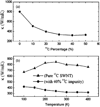 | ||
| Fig. 1 (a) Thermal conductivity vs.14C impurity percentage for (5,5) SWNT at 300 K. (b) Thermal conductivity vs. temperature for pure 12C nanotube and SWNT with 40% 14C. For further details we refer to ref. 34. Reprinted with permission from the American Institute of Physics. | ||
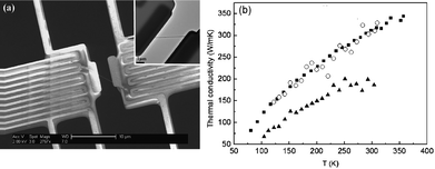 | ||
| Fig. 2 (a) A scanning electron microscope image of the test structure for thermal conductivity measurement with a nanotube on it. The inset shows the corresponding transmission electron microscope image of the same device with scale bar of 1 μm. (b) The thermal conductivity of a boron nitride nanotube (solid triangles), an isotopically pure boron nitride nanotube (solid squares) and a carbon nanotube (open circles). These tubes have similar outer diameters. Details can be found in ref. 43. Reprinted with permission from the American Physical Society. | ||
Similar to the mechanism of length dependent thermal conductivity, the origin of observable reduction of thermal conductivity in isotope-disordered NTs also can be understood from the phonon diffusive process. By using ab initio calculations with an atomistic Green's function formalism, Savić et al. studied coherent phonon transport in nanotubes with isotope disorder.44 They found that the reduction of thermal conductivity is a consequence of diffusive scattering. For low concentrations (<10%), the scattering properties of individual isotope impurities play a dominant role; while for large isotope concentrations, multiple scattering-induced interference effects were found to be prominent.
In addition to the reduction in thermal conductivity, isotope doping also changes the temperature dependence of thermal conductivity as shown in Fig. 1(b). It is obvious that the isotope impurity changes completely the temperature dependence behavior of thermal conductivity. For a pure tube, there is a maximum at about 250 K. Below this temperature, thermal conductivity increases when T is increased. Above TM, thermal conductivity decreases with increasing T. However, in the cases with isotope impurity, there is no maximum in the curve. The thermal conductivity monotonically decreases as the temperature increases. These phenomena can be understood from the phonon scattering mechanism. Increasing the temperature has two effects on thermal conductivity. On the one hand, the increase of temperature will excite more high-frequency phonons that enhance thermal conductivity. This is the “positive” effect. On the other hand, the increase of temperature will also increase phonon–phonon scattering that in turn will increase the thermal resistance, thus suppress the energy transfer, which is the “negative” effect. The thermal conductivity is determined by these two effects, which compete with each other. For a pure SWNT, in the low-temperature regime, the phonon density is small, the positive effect dominates, thus the thermal conductivity increases with increasing temperature. However, in the high-temperature regime, as more and more high frequency phonons are excited, the negative effect dominates, which results in the decrease of thermal conductivity as temperature is increased. However, in the cases with impurities, the scattering mechanism changes. In these cases, most high-frequency phonons are localized due to the impurities. The main contribution to heat conduction comes from low-energy phonons that have a long wavelength. The positive effect is largely suppressed, and in the whole temperature regime, the negative effect dominates, which leads to a decrease of thermal conductivity as the temperature is increased, as is seen in Fig. 1(b).
Vacancy and defect effects on thermal conductivity of CNT
In addition to isotope doping, practical nanotubes can have other defects, such as vacancy and conformational defects. Therefore, it is important to explore how defects influence the thermal conductivity. A new theoretical formalism for phonon transport in nanostructures using the nonequilibrium Green's function technique has been developed by Yamamoto and Watanabe.45 Using this technique, they studied thermal conductivity in carbon nanotubes, in the presence of local structure defects such as vacancies and Stone–Wales (SW) defects. They found that the universal quantization of low temperature thermal conductance can be observed, since the long wavelength acoustic phonons are not scattered by local defects. This corresponds to very weak defect effect at low temperature as shown in Fig. 3. With temperature increases, a remarkable change in defect scattering, from a quantum to a classical feature is observed. At room temperature, however, thermal conductance is critically affected by defect scattering since incident phonons are scattered by localized phonons around the defects.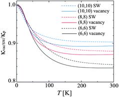 | ||
| Fig. 3 The temperature dependence of the ratio κvac(SW)/κp for the CNT with the Stone-Wales (SW) defect and vacancy. The black, red, and blue solid (dashed) curves are κvac(SW)/κp for (6,6), (8,8), and (10,10) CNTs, respectively. For further details we refer to ref. 45. Reprinted with permission from the American Physical Society. | ||
The thermal conductivity versus vacancy concentration at room temperature has also been investigated by using molecular dynamics simulations.46 The thermal conductivity decreases as the vacancy concentration increases as shown in Fig. 4. Compared with the vacancy impact on the thermal conductivity of diamond,47 it is shown that vacancies in nanotubes are not much more influential than in bulk materials. This is probably due to the fact that the strong valence double bond network in carbon nanotubes provides effective additional channels for phonons to bypass the vacancy sites.
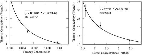 | ||
| Fig. 4 Thermal conductivity of CNTs as a function of vacancy concentration (left) and conformational defect concentration (right). Details can be found in ref. 46 Reprinted with permission from the IOP. | ||
Similarly, conformational defects, such as (5,7,7,5) where four hexagons change into two pentagons and two hexagons, can also reduce the thermal conductivity significantly as shown in Fig. 4. Compared with vacancies, the (5,7,7,5) defect is a milder form of point defect, since it does not change the basic bonding characteristic and induces much less structural deformation. Thus, the decrease in thermal conductivity is less than in the case of vacancies.
The impact of nitrogen substitutional impurities on the CNT thermal conductivity was studied by Mingo et al. by using an ab initio density functional approach.48 They found that most of the reduction of transmission takes place at the higher frequency part of the phonon spectrum, thus its effect on thermal conductance is only noticeable at high temperature. This is because the force constants of the impurity system are very similar to those of the pure carbon system.
The surface chemisorbed molecules also can be treated as one type of doping. Pedgett and Brenner49 studied the room temperature thermal conductivity of carbon nanotubes that have been functionalized by chemical attachment of phenyl rings through covalent bonding at random positions as a function of adsorption density. As shown in Fig. 5, they found that there is a rapid drop in thermal conductivity with chemisorptions, where chemisorptions to as little as 1% of the CNT atoms reduces the thermal conductivity by over a factor of 3.
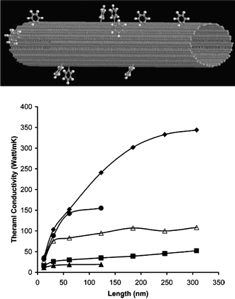 | ||
| Fig. 5 Thermal conductivity versus nanotube length for various degrees of functionalization. Diamonds 0%, circles 0.25%, open triangles 1%, squares 5%, and triangles 10% functionalized. For details, please refer to ref. 49. Reprinted with permission from the American Chemical Society. | ||
Doping effects on thermal conductivity and thermoelectric figure of merit of nanowires
Silicon nanowires (SiNWs) have attracted a great attention in recent years because of their excellent electrical and mechanical properties50 and their potential applications in many areas including biosensors,51,52 electronic devices53,54 and solar PVs.55,56 SiNWs are an appealing choice because of their ideal interface compatibility with conventional Si-based devices.57 It is found that the electronic properties of SiNWs depend significantly on the surface and growth direction. These special properties are partially due to the high surface-to-volume ratio in nanomaterials.58,59Thermal conductivity of nanowires
Like some other nanomaterials, the silicon nanowires might be used as thermoelectric materials.60,61,62,63 The performance of thermoelectric materials depends on the figure of merit ZT: ZT = σTS2/κ, where S, T, σ, and κ are the Seebeck coefficient, absolute temperature, electronic conductivity and total thermal conductivity, respectively. ZT can be increased by increasing S or σ, or decreasing κ. Unfortunately, in conventional materials, it is difficult to improve ZT. First, a simple increase in S for general materials will lead to a simultaneous decrease in σ.64 Also, an increase in σ leads to a comparable increase in the electronic contribution to κ. An alternative way to increase ZT is to reduce the thermal conductivity without affecting electronic property.65 Moreover, ultra-low thermal conductivity is also required to prevent the back-flow of heat from the hot end to the cool end. Therefore, reduction of thermal conductivity is crucial in thermoelectric applications.Due to the size effect and high surface to volume ratio, the thermal conduction properties of silicon nanostructures differ substantially from those of bulk materials.66 Volz and Chen investigated the thermal conductivity of silicon nanowires based on molecular dynamic simulations using the Green–Kubo method, and found that thermal conductivity of individual silicon nanowires is more than 2 orders of magnitude lower than the bulk value.67,68 Li et al.69 have also reported a significant reduction of thermal conductivity in silicon nanowires compared to the thermal conductivity in bulk silicon experimentally, and strong diameter dependence was observed as shown in Fig. 6. This is due to the following facts. Firstly, the low frequency phonons, whose wavelengths are longer than the length of a nanowire, cannot survive in nanowires. Therefore, the low frequency contribution to thermal conductivity, which is very substantial and significant in bulk material, is largely reduced. Secondly, because of the large surface to volume ratio, boundary scattering in quasi-1D structures is also significant. More experimental and theoretical activities have been inspired to explore this direction, including the theoretical prediction of the thermal conductivity of Ge nanowires,70 molecular dynamics simulation of nanofilms,71 and experimental measurement of the thermal conductivity of Si/SiGe superlattice nanowires.72 The low temperature (<2 K) thermal conductance of individual suspended SiNWs was measured by Bourgeois et al.73 Wang et al. observed the pure phonon confinement effect in germanium nanowires by measurement of Raman spectra for different size germanium nanowires with different excitation laser powers and wavelengths.74 An analytical formula including surface scattering and the size confinement effects of phonon transport is proposed by Liang and Li75 to describe the size dependence of thermal conductivity in NWs and other nanoscale structures. In recent experiments,76,77 high thermoelectric figure of merit has been achieved in SiNWs, which is about a 100-fold improvement over the value of bulk silicon. And the mesoscopic size effect on the low temperature thermal conductance of SiNW has been demonstrated experimentally.78 In addition, Ponomareva et al.79 studied the phonon confinement effect in SiNWs by using molecular dynamics simulations. They found that the phonon group velocity, mode distribution and phonon-scattering effects are independent on the nanowire diameter. Donadio and Galli80 studied heat transport in SiNWs systematically, by using molecular dynamics simulation, lattice dynamics, and Boltzmann transport equation calculations. It was demonstrated that the disordered surfaces, nonpropagating modes analogous to heat carriers, together with decreased lifetimes of propagating modes are responsible for the reduction of thermal conductivity in SiNWs. The Monte Carlo simulation technique has also been utilized to predict the thermal conductivity of silicon nanowires81 and nanocomposites.82 Other theoretical results on thermal conductivity of nanoscale silicon thin films,83 square silicon nanowires84 and silica nanowires85 have also been reported.
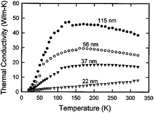 | ||
| Fig. 6 Measured thermal conductivity of different diameter Si nanowires. For further details we refer to ref. 69. Reprinted with permission from the American Institute of Physics. | ||
Isotopic doping effect on thermal conductivity of NWs
The low thermal conductivity of SiNWs is of particular interest for thermoelectric application. The thermal conductivity of SiNWs is lower than that of the bulk silicon, whereas it is still larger than the reported ultralow thermal conductivity (0.05 W m−1 K) found in layered materials.86 So, it is indispensable to reduce the thermal conductivity of SiNWs further in order to achieve higher thermoelectric performance. Yang et al. have proposed two isotope doping methods for reduction of thermal conductivity of SiNWs.87 The first one is to dope SiNWs with isotope impurity randomly. The second one is to build isotopic-superlattice structured SiNWs. In silicon isotopes, 28Si is with the highest natural abundance (92%), then 29Si and 30Si with 5% and 3%, respectively.88 Besides these three, 42Si and 43Si are also observed.89 Here the effect of doping 29Si and 42Si to 28Si NWs are shown, because the mass difference between 42Si and 28Si is large, which provides a good chance to study the mass influence on thermal conductivities.The effect of randomly distributed isotopic atoms on the thermal conductivity of 28Si NWs is shown in Fig. 7. The curve of thermal conductivity decreases first to reach a minimum and then increases as the percentage of isotope impurity atoms changes from zero to a hundred. At low isotopic percentage, the small ratio of impurity atoms can induce large reduction on conductivity. For example, in the case of 28Si0.9842Si0.02, its thermal conductivity is only 65% of that of pure 28Si NW. In contrast to the high sensitivity at the two ends, the thermal conductivity versus isotopic concentration curves are almost flat at the center part, as shown in Fig. 7, where the value of thermal conductivity is only 27% (42Si doping) or 77% (29Si doping) of that of pure 28Si NW. The calculated thermal conductivity of SiNW with natural isotopic abundance, 5% 29Si and 3% 30Si, is around 86% of pure 28Si NW, which is close to the experimental results in bulk Si,90,91 which is about 10% reduction. The similar impact of impurities on the thermal conductivity of SiNWs is also reported by using first-principles calculations.92
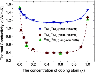 | ||
| Fig. 7 Thermal conductivity of SiNWs versus the percentage of randomly doping isotope atoms at 300 K. SiNWs are along the (100) direction with cross sections of (3 × 3) unit cells (lattice constant is 0.543 nm). The results, by the Nosé–Hoover, method coincide with those by Langevin methods indicating that the conclusions are independent of the heat bath used. Details are given in ref. 87. Reprinted with permission from the American Chemical Society. | ||
It has been shown,93,94 that superlattices are efficient structures to get ultra low thermal conductivity. However for structures built from different crystal materials, the relatively high interface energy will limit the stability of these structures. The isotopic-superlattice (IS) is a good one to reduce the thermal conductivity without destroying the stability. The thermal conductivity of IS structured NWs (shown in Fig. 8) which consists of alternating 28Si/42Si or 28Si/29Si layers along the longitudinal direction are shown in Fig. 9. As expected, the thermal conductivity decreases as the period length decreases, which means the number of interfaces increases. The thermal conductivity reaches a minimum when the period length is 1.09 nm. This is consistent with the fact that increasing the number of interfaces for a fixed length will enhance the interface scattering which gives rise to the reduction of the thermal conductivity. With a period length smaller than 1.09 nm, the thermal conductivity increases rapidly as the period length decreases. This anomalous increase in thermal conductivity can be understood from the phonon density of states (DOS). When period length is 2.17 nm, there is an obvious mismatch in the DOS spectra, both at low frequency bands and high frequency bands, resulting in very low thermal conductivity. On the contrary, the DOS spectra overlap perfectly for IS structured SiNW the period length of which is 0.27 nm. The good match in the DOS comes from the collective vibrations of different mass layers which is harder to build in longer superlattice period structures. The match/mismatch of the DOS spectra between the different mass layers controls the heat current.
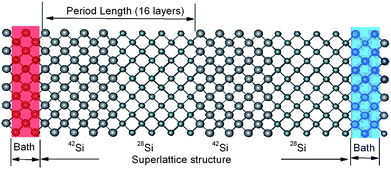 | ||
| Fig. 8 Schematic picture of the IS structured SiNW. The period length is 2.17 nm (16 layers) here. Atoms with different mass are denoted by the different size. For further details we refer to ref. 87. Reprinted with permission from the American Chemical Society. | ||
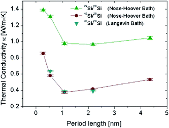 | ||
| Fig. 9 Thermal conductivity of the superlattice SiNWs versus the period length at 300 K. SiNWs are along the (100) direction with cross sections of (3 × 3) unit cells (lattice constant is 0.543 nm). For details of the parameters we refer to ref. 87. Reprinted with permission from the American Chemical Society. | ||
The growth of isotopically controlled silicon nanowires by the vapor–liquid–solid mechanism has been done recently.95 The growth is accomplished by using silane precursors 28SiH4, 29SiH4 and 30SiH4 synthesized from SiF4 isotopically enriched in a centrifugal setup. And the effect of isotope doping on Si–Si LO phonon has also been investigated, as shown in Fig. 10. The corresponding experimental measurement of thermal conductivity is on-going.
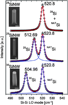 | ||
| Fig. 10 Raman scattering spectra of monoisotopic SiNWs. For details of the Figure we refer to ref. 95. Reprinted with permission from Nano Today, Elsevier. | ||
Isotopic doping effect on thermoelectric figure of merit of NW
In order to obtain the figure of merit of nanowires numerically, one can calculate the Seebeck coefficient, electrical conductivity and electron thermal conductivity by using first-principles electronic structure calculations and the Boltzmann transport equation, and the phonon thermal conductivity by using molecular dynamics.The dependence of the thermoelectric figure of merit, ZT of SiNW on isotope doping concentration is shown in Fig. 11.96 The ZT values increase with 29Si concentration, reach a maximum and then decrease. This phenomenon is from the isotope doping effect on lattice thermal conductivity. At low isotopic percentage, the small ratio of isotope atoms can induce large increase in ZTMax. For instance, in the case of 28Si0.829Si0.2 NW, namely, about 20% 29Si, its ZTMax increases with 15% from that of pure 28Si NW; and with 50% 29Si doping (28Si0.529Si0.5 NW) the ZTMax can increase from 0.81 to 1.06. Thus, isotope doping is a promising method to enhance further ZT of nanoscale materials.
![Isotopic concentration dependent thermoelectric figure of merit, ZT, for SiNWs along [110] direction with fixed cross section area of 2.3 nm2. For details of the parameters we refer to ref. 96. Reprinted with permission from the American Institute of Physics.](/image/article/2010/NR/c0nr00095g/c0nr00095g-f11.gif) | ||
| Fig. 11 Isotopic concentration dependent thermoelectric figure of merit, ZT, for SiNWs along [110] direction with fixed cross section area of 2.3 nm2. For details of the parameters we refer to ref. 96. Reprinted with permission from the American Institute of Physics. | ||
Composition dependent thermal conductivity of SiGe nanowires and nanocrystals
In addition to isotopic doped semiconductors, compound semiconductors are other possible structures that have low thermal conductivity. Silicon germanium alloys have long been used in thermoelectric modules for deep-space missions to convert radio-isotope heat into electricity. Silicon and germanium can form a continuous series of substitutional solid, Si1−xGex over the entire compositional range of 0 ≤ x ≤ 1. These semiconductor alloys offer a continuously variable system with a wide range of crystal lattices and band gaps, leading to various electrical and optical properties. For instance, the continuous variation in the energy band gap in Si1−xGex provides great opportunities for Si optoelectronics because it potentially allows emission and detection of the photons in a large wavelength range. Recently, single crystalline Si1−xGex NWs have been successfully grown and the electronic band gap modulation with composition has been reported.97 Lauhon et al.98 reported the heteroepitaxial growth of crystalline Si–Ge and Ge–Si core–shell structures. The experimental synthesis of Si1−xGex NWs provides intriguing opportunities for the development of novel nano devices. The tenability of those properties makes this kind of semiconductor systems very attractive for industrial applications. It is now well recognized that nanoscale Si1−xGex NWs have immense potential application for electronic and optoelectronic devices within well-established silicon based microelectronic technology. Moreover, as both Si and Ge belong to the same group in the periodic table, and have the same crystal structure, Si1−xGex NW seems to display total solubility.Fig. 12 shows the thermal conductivity κ of Si1−xGex NWs versus Ge content x at room temperature.99 The lowest κ is 0.59W m−1 K calculated with a Langevin heat bath, which is 18% of that of pure SiNW calculated with the same heat bath, and is 15% of that of pure SiNW calculated with a Nosé–Hoover heat bath. At the two ends of the curves, the thermal conductivity shows a very sensitive dependence on x and follows an exponential decay, which is caused by the localization of high frequency phonons by the impurity. It is quite interesting that the thermal conductivity can be reduced by 50% with only 5% Ge atoms (Si0.95Ge0.05 NW).
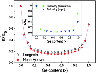 | ||
| Fig. 12 The thermal conductivity vs. Ge content x at 300 K. Here κ is the thermal conductivity of Si1−xGex NWs, and κ0 is the corresponding thermal conductivity of pure Si NW. The simulation and experimental results for bulk Si1−xGex alloy are also shown here. Although the thermal conductivity of NW is about two orders of magnitude smaller than that of bulk material, the dependence of κ on Ge atom content is similar. For details of the parameters we refer to ref. 99. Reprinted with permission from the American Institute of Physics. | ||
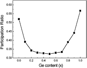
To depict the localization phenomenon quantitatively, people usually use the participation ratio P,100 which is O(1) for delocalized states and O(1/N) for localized states. The participation ratio versus Ge content x is shown in Fig. 13. For both pure Si NW and pure Ge NW, a high participation ratio appears, indicating the delocalized characteristics of phonon modes and corresponds to high thermal conductivity. However, in the Si1−xGex NWs (0 < x < 1), with the impurity concentration increasing, the participation ratio decreases significantly, indicating strong localization due to impurity scattering and corresponds to low thermal conductivity. The Ge content dependent participation ratio is consistent with the changes in thermal conductivity.
 | ||
| Fig. 13 The participation ratio vs. Ge content x for Si1−xGex NWs. For details of the parameters we refer to ref. 99. Reprinted with permission from the American Institute of Physics. | ||
From the calculated low thermal conductivity, it is shown that the maximal obtainable figure of merit can be increased by a factor of about 4–5 in Si0.5Ge0.5NWs, compared with the corresponding values in pure silicon nanowires. Combine with the experimental measured ZT of n-type SiNW which is about 0.6–1.0, it is most likely that we may obtain a high ZT value of about 2.4∼4.0 in n-type Si1−xGex NWs.
In addition to SiGe nanowires, it has been observed experimentally that when the Ge content in Si1−xGex nanocomposites increases from 5% to 20%, the thermal conductivity of p-type silicon germanium alloy101 and n-type alloy102 decreases obviously. It is found that nano-size interfaces are not as effective as point defects in scattering phonons with wavelengths shorter than 1 nm. Fig. 14 shows that only a 5 at.% Ge replacing Si is very efficient in scattering phonons shorter than 1 nm, giving rise to a further thermal conductivity reduction by a factor of 2.
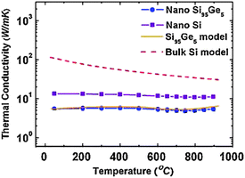 | ||
| Fig. 14 Temperature dependent thermal conductivity of nanostructured Si (filled squares), nanostructured Si95Ge5 (filled circles) and bulk Si model. For details of the parameters we refer to ref. 102. Reprinted with permission from the American Physical Society. | ||
Defect effect on thermal conductivity and thermoelectric property of NWs
Nanostructures such as nanowires usually have both natural and artificial defects. Defects can lead to the localization of acoustic modes in the vicinity of the defects. This will cause additional scattering of the phonon transport, which results in the change of the thermal conductance for ballistic phonon transport. Several groups103,104 have derived expressions of thermal conductance for ballistic phonon transport at a low temperature regime, and found that the thermal conductance at low temperature is quantized in a universal unit π2k2B/3h, analogous to the well-known quantized electronic conductance unit 2e2/h. These theories are in good agreement with experiment.105 By using the scattering-matrix method, Chen et al. studied the low temperature thermal conductance in nanowires.106 It is found that the behavior of the thermal conductance versus temperature is qualitatively different for different types of defects. When the defect is void, the universal quantum thermal conductance and the decrease of the thermal conductance at low temperature can be clearly observed. However, when the structural defect consists of clamped material, the quantized thermal conductance cannot be observed, and the thermal conductance increases monotonically with increasing temperature.Based on atomistic simulations of electron and phonon transport, Markussen et al.107 found that the presence of an alkyl molecule or a nanowire branch will lead to a reduction of the thermal conductivity δκ and a reduction of the electronic conductivity δσ. At room temperature, it is demonstrated that the ratio δκ/δσ > 50 for the alkyl functionalized SiNWs and δκ/δσ > 20 for a nanotree. By engineering the SiNW surfaces, it is obvious that people can reduce the phonon thermal conductivity while keeping the electronic conductivity almost unaffected. Thus the surface decorated SiNWs are promising candidates for nanoscale thermoelectric applications.
Doping effect on thermal conductivity and thermoelectric property of graphene
Graphene nanoribbons (GNR) are a new type of quasi-one-dimensional carbon material, which can be easily obtained either by cutting mechanically exfoliated graphenes,108 or by patterning epitaxially growth graphenes.109 As a novel one-atom-thick material, GNRs have numerous unique properties different from those of other nano-materials110,111 GNRs exhibit an extremely high carrier mobility,112 which demonstrates their outstanding ballistic transport properties,113,114 and GNRs are found to have a giant Seebeck coefficient.115Moreover, a high thermal conductivity (as high as 5000 W m−1 K−1)116,117 has been demonstrated in graphene. Meanwhile, it has been demonstrated that the umklapp, defects and edge scattering have a remarkable impact on the electrical118 and thermal conductance119 in graphene, and large thermal rectification has been observed in asymmetric graphene ribbons.120,121 Jiang et al. demonstrated that the thermal conductance of graphene sheet depends weakly on the direction angle of the thermal flux due to the directional dependence of group velocities of the phonon modes in the graphene, originating from the D6h symmetry in the honeycomb structure.122 When the D6h symmetry is broken, the thermal conductance shows more obvious anisotropy and the value is about 40% smaller than that of the graphene at room temperature. In addition, a T1.5 dependence at low temperature is observed, which is due to the contribution of the flexure mode.
Isotopic doping effect on the thermal conductivity of graphene
The isotopic doping effect on the thermal conductivity of graphene nanoribbons is studied by classical molecular dynamics simulation with quantum correction.123 It is found that in low isotopic doping region, the thermal conductivity decreases rapidly with increasing doping, and 10% doping can yield 50% reduction of the value of thermal conductivity; while in the high isotopic doping region, the thermal conductivity decreases slowly with further increasing doping. The underlying mechanism is that a single isotopic doping center can localize phonon modes which will reduce thermal transport. So, generally the thermal conductivity will decrease after isotopic doping. Moreover, the thermal conductivity temperature dependent behavior also depends on the isotopic doping.In addition to the isotope randomly doping, the thermal conductivity of isotopic superlattice graphene nanoribbons was also studied.124 The thermal transport property of the isotopic superlattice graphene strongly depends on the superlattice period length and the isotopic mass. With the period length decreases, the thermal conductivity undergoes a transition from decreasing to increasing, which is explained by analyzing the phonon transmission coefficient, and a larger mass difference induces smaller thermal conductivity.
Vacuum effect on thermoelectric figure of merit of graphene
The impact of disorder defect on the thermoelectric figure of merit of graphene has been investigated by using density functional theory calculations combined with the nonequilibrium Green's function method.125 It is found that the figure of merit can be, remarkably, enhanced five times by randomly introducing vacancies to the graphene. From Fig. 15, a room temperature ZT as high as 2 can be achieved by disturbing full saturation of the hydrogen–carbon bonds in perfect graphene nano-ribbons. This is indeed the case in experiments, as achieving full saturation is extremely difficult. The mechanism for the enhancement of thermoelectric performance is the reduction of the lattice thermal conductance. More interestingly, it is found that ZT increases linearly with temperature. This is of great importance as it indicates that higher temperature can give better thermoelectric performance in graphene nano-ribbons.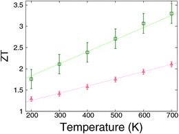 | ||
| Fig. 15 Temperature dependence of ZT values for disordered grapheme. m = 5 (triangles) and m = 10 (squares). For details of the parameters we refer to ref. 125. Reprinted with permission from the American Institute of Physics. | ||
Outlook
The present article tries to give an overview of the thermal properties of nanomaterials. The thermal transport in a low dimensional system has attracted wide research interest in the last decade. These low dimensional nano-structured materials are promising platforms to verify fundamental phonon transport theories. Moreover, the study of the thermal properties of nanomaterials is also important for potential applications. It has been shown that the thermal properties in nanostructures differ significantly from those in bulk materials because the phonon characteristic lengths are comparable to the characteristic length of the nanostructures. Doping has a remarkable impact on thermal conductance and thermoelectric properties of nanomaterials.Compared with ten years ago, we have a comprehensive understanding of the impact of doping on thermal conductance and the thermoelectric properties of nanoscale materials. However, there are still many open questions; for instance, a quantitative expression for the doping effect on the figure of merit. Further experimental and theoretical studies on fundamental mechanisms will be help greatly to advance the field.
References
- A. Dhar, Adv. Phys., 2008, 57, 457 CrossRef CAS.
- B. Li and J. Wang, Phys. Rev. Lett., 2003, 91, 044301 CrossRef.
- L. Wang and B. Li, Phys. World, 2008, 21, 27 Search PubMed.
- B. Li, L. Wang and G. Casati, Phys. Rev. Lett., 2004, 93, 184301 CrossRef.
- N. Yang, N. Li, L. Wang and B. Li, Phys. Rev. B: Condens. Matter Mater. Phys., 2007, 76, 020301 CrossRef.
- B. Li, L. Wang and G. Casati, Appl. Phys. Lett., 2006, 88, 143501 CrossRef.
- W.-C. Lo, L. Wang and B. Li, J. Phys. Soc. Jpn., 2008, 77, 054402 CrossRef.
- L. Wang and B. Li, Phys. Rev. Lett., 2007, 99, 177208 CrossRef.
- L. Wang and B. Li, Phys. Rev. Lett., 2008, 101, 267203 CrossRef.
- C. W. Chang, D. Okawa, A. Majumdar and A. Zettl, Science, 2006, 314, 1121 CrossRef CAS.
- G. Wu and B. Li, Phys. Rev. B: Condens. Matter Mater. Phys., 2007, 76, 085424 CrossRef.
- N. Yang, G. Zhang and B. Li, Appl. Phys. Lett., 2008, 93, 243111 CrossRef.
- Thermoelectrics Handbook: Macro To Nano, ed. D. M. Rowe, Taylor & Francis Group, Boca Raton, FL, 2006 Search PubMed.
- G. Chen, J. Nanopart. Res., 2000, 2, 199 CrossRef CAS.
- J. Shiomi and S. Maruyama, Phys. Rev. B: Condens. Matter Mater. Phys., 2006, 73, 205420 CrossRef.
- D. G. Cahill, W. K. Ford, K. E. Goodson, G. D. Mahan, A. Majumder, H. J. Maris, R. Merlin and S. R. Phillpot, J. Appl. Phys., 2003, 93, 793 CrossRef CAS.
- S. Iijima, Nature, 1991, 354, 56 CrossRef CAS.
- M. M. J. Treacy, T. W. Ebbesen and J. M. Gibson, Nature, 1996, 381, 678 CrossRef CAS.
- E. W. Wong, P. E. Sheehan and C. M. Lieber, Science, 1997, 277, 1971 CrossRef CAS.
- R. Satio, G. Dresselhaus, and M. S. Dresselhaus, Physical Properties of Carbon Nanotubes, Imperial College Press, London, 1999 Search PubMed.
- S. J. Tans, A. R. M. Verschueren and C. Dekker, Nature, 1998, 393, 49 CrossRef CAS.
- A. G. Rinzler, J. H. Hafner, P. Nikolaev, L. Lou, S. G. Kim, D. Tomanek, P. Nordlander, D. T. Colbert and R. E. Smalley, Science, 1995, 269, 1550 CrossRef CAS.
- W. A. de Heer, A. Chatelain and D. Ugrate, Science, 1995, 270, 1179 CrossRef CAS.
- J. Hone, M. Whitney, C. Piskoti and A. Zettl, Phys. Rev. B: Condens. Matter Mater. Phys., 1999, 59, R2514 CrossRef CAS.
- D. J. Yang, Q. Zhang, G. Chen, S. F. Yoon, J. Ahn, S. G. Wang, Q. Zhou, Q. Wang and J. Q. Li, Phys. Rev. B: Condens. Matter Mater. Phys., 2002, 66, 165440 CrossRef.
- P. Kim, L. Shi, A. Majumdar and P. L. McEuen, Phys. Rev. Lett., 2001, 87, 215502 CrossRef CAS.
- Y.-K. Kwon, S. Berber and D. Tomanek, Phys. Rev. Lett., 2004, 92, 015901 CrossRef.
- G. Zhang and B. Li, J. Phys. Chem. B, 2005, 109, 23823 CrossRef CAS.
- S. Berber, Y.-K. Kwon and D. Tománek, Phys. Rev. Lett., 2000, 84, 4613 CrossRef CAS.
- M. A. Osman and D. Srivastava, Nanotechnology, 2001, 12, 21 CrossRef CAS.
- T. Yamamoto, S. Watanabe and K. Watanabe, Phys. Rev. Lett., 2004, 92, 075502 CrossRef.
- D. Donadio and G. Galli, Phys. Rev. Lett., 2007, 99, 255502 CrossRef.
- A. V. Savin, Y. S. Kivshar and B. Hu, Europhys. Lett., 2009, 88, 26004 CrossRef.
- G. Zhang and B. Li, J. Chem. Phys., 2005, 123, 114714 CrossRef.
- S. Maruyama, Phys. B, 2002, 323, 193 CrossRef CAS.
- Z.-H. Yao, J.-S. Wang, B. Li and G.-R. Liu, Phys. Rev. B: Condens. Matter Mater. Phys., 2005, 71, 085417 CrossRef.
- A. Savin, B. Hu and Y. Kivshar, Phys. Rev. B: Condens. Matter Mater. Phys., 2009, 80, 195423 CrossRef.
- G. Zhang and B. Li, J. Chem. Phys., 2005, 123, 014705 CrossRef.
- V. G. Plekhanov, Mater. Sci. Eng., R, 2001, 35, 139 CrossRef.
- G. Zhang, W. Duan and B.-L. Gu, Appl. Phys. Lett., 2002, 80, 2589 CrossRef CAS.
- G. Zhou and W. Duan, J. Nanosci. Nanotechnol., 2005, 5, 1421 CrossRef CAS.
- T. D. Ositinskaya, A. P. Podoba and S. V. Shmegera, Diamond Relat. Mater., 1993, 2, 1500 CrossRef CAS.
- C. W. Chang, A. M. Fennimore, A. Afanasiev, D. Okawa, T. Ikuno, H. Garcia, D. Li, A. Majumdar and A. Zettl, Phys. Rev. Lett., 2006, 97, 085901 CrossRef CAS.
- I. Savić, N. Mingo and D. A. Stewart, Phys. Rev. Lett., 2008, 101, 165502 CrossRef.
- T. Yamamoto and K. Watanabe, Phys. Rev. Lett., 2006, 96, 255503 CrossRef.
- J. Che, T. Cagin and W. A. Goddard III, Nanotechnology, 2000, 11, 65 CrossRef CAS.
- J. Che, Tahir Cagın, W. Deng and W. A. Goddard III, J. Chem. Phys., 2000, 113, 6888 CrossRef CAS.
- N. Mingo, D. A. Stewart, D. A. Broido and D. Srivastava, Phys. Rev. B: Condens. Matter Mater. Phys., 2008, 77, 033418 CrossRef.
- C. W. Padgett and D. W. Brenner, Nano Lett., 2004, 4, 1051 CrossRef CAS.
- Y. Xia, P. Yang, Y. Sun, Y. Wu, B. Mayers, B. Gates, Y. Fin, F. Kim and H. Yan, Adv. Mater., 2003, 15, 353 CrossRef CAS.
- Y. Cui, Q. Wei, H. Park and C. M. Lieber, Science, 2001, 293, 1289 CrossRef CAS.
- G.-J. Zhang, G. Zhang, H. J. Chua, R.-E. Chee, E. H. Wong, A. Agarwal, K. D. Buddharaju, N. Singh, Z. Gao and N. Balasubramanian, Nano Lett., 2008, 8, 1066 CrossRef CAS.
- J. Xiang, W. Lu, Y. Hu, Y. Wu, H. Yan and C. M. Lieber, Nature, 2006, 441, 489 CrossRef CAS.
- S. C. Rustagi, N. Singh, Y. F. Lim, G. Zhang, S. Wang, G. Q. Lo, N. Balasubramanian and D. L. Kwong, IEEE Electron Device Lett., 2007, 28, 909 CrossRef CAS.
- L. Hu and G. Chen, Nano Lett., 2007, 7, 3249 CrossRef CAS.
- J. S. Li, H. Y. Yu, S. M. Wong, G. Zhang, X. W. Sun, L. Q. Lo and D. L. Kwong, Appl. Phys. Lett., 2009, 95, 033102 CrossRef.
- Y. Li, F. Qian, J. Xiang and C. M. Lieber, Mater. Today, 2006, 9, 18 CrossRef CAS.
- D. Yao, G. Zhang and B. Li, Nano Lett., 2008, 8, 4557 CrossRef CAS.
- D. Yao, G. Zhang, G.-Q. Lo and B. Li, Appl. Phys. Lett., 2009, 94, 113113 CrossRef.
- X. Sun, Z. Zhang and M. S. Dresselhaus, Appl. Phys. Lett., 1999, 74, 4005 CrossRef CAS.
- O. Rabina, Y. M. Lin and M. S. Dresselhaus, Appl. Phys. Lett., 2001, 79, 81 CrossRef CAS.
- G. Zhang, Q. Zhang, C.-T. Bui, G.-Q. Lo and B. Li, Appl. Phys. Lett., 2009, 94, 213108 CrossRef.
- G. Zhang, Q.-X. Zhang, D. Kavitha and G.-Q. Lo, Appl. Phys. Lett., 2009, 95, 243104 CrossRef.
- L. D. Hicks and M. S. Dresselhaus, Phys. Rev. B: Condens. Matter, 1993, 47, 16631 CrossRef CAS.
- A. Majumdar, Science, 2004, 303, 777 CrossRef CAS.
- A. S. Henry and G. Chen, J. Comput. Theor. Nanosci., 2008, 5, 1 CrossRef.
- S. G. Volz and G. Chen, Appl. Phys. Lett., 1999, 75, 2056 CrossRef CAS.
- S. G. Volz and G. Chen, Phys. Rev. B: Condens. Matter Mater. Phys., 2000, 61, 2651 CrossRef CAS.
- D. Li, Y. Wu, P. Kim, L. Shi, P. Yang and A. Majumdar, Appl. Phys. Lett., 2003, 83, 2934 CrossRef.
- N. Mingo, L. Yang, D. Li and A. Majumdar, Nano Lett., 2003, 3, 1713 CrossRef CAS.
- Z. Zhong, X. Wang and J. Xu, Numer. Heat Transfer, Part B, 2004, 46, 429 Search PubMed.
- D. Li, Y. Wu, R. Fan, P. Yang and A. Majumdar, Appl. Phys. Lett., 2003, 83, 3186 CrossRef CAS.
- O. Bourgeois, T. Fourniew and J. Chaussy, J. Appl. Phys., 2007, 101, 016104 CrossRef.
- X. Wang, A. Shakouri, B. Yu, X. Sun and M. Meyyappan, J. Appl. Phys., 2007, 102, 014304 CrossRef.
- L. H. Liang and B. Li, Phys. Rev. B: Condens. Matter Mater. Phys., 2006, 73, 153303 CrossRef.
- A. I. Hochbaum, R. Chen, R. D. Delgado, W. Liang, E. C. Garnett, M. Najarian, A. Majumdar and P. Yang, Nature, 2008, 451, 163 CrossRef CAS.
- A. I. Boukai, Y. Bunimovich, J. T. Kheli, J.-K. Yu, W. A. Goddard III and J. R. Heath, Nature, 2008, 451, 168 CrossRef CAS.
- J. S. Heron, T. Fournier, N. Mingo and O. Bourgeois, Nano Lett., 2009, 9, 1861 CrossRef CAS.
- I. Ponomareva, D. Srivastava and M. Menon, Nano Lett., 2007, 7, 1155 CrossRef CAS.
- D. Donadio and G. Galli, Phys. Rev. Lett., 2009, 102, 195901 CrossRef.
- Y. Chen, D. Li, J. R. Lukes and A. Majumdar, J. Heat Transfer, 2005, 127, 1129 CrossRef.
- M.-S. Jeng, R. Yang, D. Song and G. Chen, J. Heat Transfer, 2008, 130, 042410 CrossRef.
- X.-L. Feng, Z.-X. Li and Z.-Y. Guo, Nanoscale Microscale Thermophys. Eng., 2003, 7, 153 Search PubMed.
- X. Lu and J. Chu, J. Appl. Phys., 2006, 100, 014305 CrossRef.
- S. S. Mahajan, G. Subbarayan and B. G. Sammakia, Phys. Rev. E: Stat., Nonlinear, Soft Matter Phys., 2007, 76, 056701 CrossRef.
- C. Chiritescu, D. G. Cahill, N. Nguyen, D. Johnson, A. Bodapati, P. Keblinski and P. Zschack, Science, 2007, 315, 351 CrossRef CAS.
- N. Yang, G. Zhang and B. Li, Nano Lett., 2008, 8, 276 CrossRef CAS.
- K. J. R. Rosman and P. D. P. Taylor, Pure Appl. Chem., 1998, 70, 217 CrossRef CAS.
- J. Fridmann, et al. , Nature, 2005, 435, 922 CrossRef CAS.
- T. Ruf, R. W. Henn, M. Asen-Palmer, E. Gmelin, M. Cardona, H.-j. Pohl, G. G. Devyatych and P. G. Sennikov, Solid State Commun., 2003, 127, 257 CrossRef CAS.
- D. G. Cahill and Fumiya Watanabe, Phys. Rev. B: Condens. Matter Mater. Phys., 2004, 70, 235322 CrossRef.
- T. M. Gibbons and S. K. Estreicher, Phys. Rev. Lett., 2009, 102, 255502 CrossRef CAS.
- X. Y. Yu, G. Chen, A. Verma and J. S. Smith, Appl. Phys. Lett., 1995, 67, 3554 CrossRef CAS.
- S. T. Huxtable, A. R. Abramson, C.-L. Tien and A. Majumdar, Appl. Phys. Lett., 2002, 80, 1737 CrossRef CAS.
- O. Moutanabbir, S. Senz, Z. Zhang and Ulrich Gösele, Nano Today, 2009, 4, 393 CrossRef CAS.
- L. Shi, D. Yao, G. Zhang and B. Li, Appl. Phys. Lett., 2009, 95, 063102 CrossRef.
- J.-E. Yang, C.-B. Jin, C.-J. Kim and M.-H. Jo, Nano Lett., 2006, 6, 2679 CrossRef CAS.
- L. J. Lauhon, M. S. Gudiksen, D. Wang and C. M. Lieber, Nature, 2002, 420, 57 CrossRef CAS.
- J. Chen, G. Zhang and B. Li, Appl. Phys. Lett., 2009, 95, 073117 CrossRef.
- A. Bodapati, P. K. Schelling, S. R. Phillpot and P. Keblinski, Phys. Rev. B: Condens. Matter Mater. Phys., 2006, 74, 245207 CrossRef.
- G. Joshi, H. Lee and Y. Lan, et al. , Nano Lett., 2008, 8, 4670 CrossRef CAS.
- G. H. Zhu, H. Lee and Y. C. Lan, et al. , Phys. Rev. Lett., 2009, 102, 196803 CrossRef CAS.
- L. G. C. Rego and G. Kirczenow, Phys. Rev. Lett., 1998, 81, 232 CrossRef CAS.
- W.-X. Li, K.-Q. Chen, W. Duan, J. Wu and B.-L. Gu, Appl. Phys. Lett., 2004, 85, 822 CrossRef CAS.
- K. Schwab, E. A. Henriksen, J. M. Worlock and M. L. Roukes, Nature, 2000, 404, 974 CrossRef CAS.
- K.-Q. Chen, W.-X. Li, W. Duan, Z. Shuai and B.-L. Gu, Phys. Rev. B: Condens. Matter Mater. Phys., 2005, 72, 045422 CrossRef.
- T. Markussen, A.-P. Jauho and M. Brandbyge, Phys. Rev. Lett., 2009, 103, 055502 CrossRef.
- K. S. Novoselov, A. K. Geim, S. V. Morozov, D. Jiang, Y. Zhang, S. V. Dubonos, I. V. Grigorieva and A. A. Firsov, Science, 2004, 306, 666 CrossRef CAS.
- C. Berger, Z. Song, X. Li, X. Wu, N. Brown, C. Naud, D. Mayou, T. Li, J. Hass, A. N. Marchenkov, E. H. Conrad, P. N. First and W. A. De Heer, Science, 2006, 312, 1191 CrossRef CAS.
- A. H. Castro Neto, F. Guinea, N. M. R. Peres, K. S. Novoselov and A. K. Geim, Rev. Mod. Phys., 2009, 81, 109 CrossRef CAS.
- A. K. Geim and K. S. Novoselov, Nat. Mater., 2007, 6, 183 CrossRef CAS.
- J. H. Chen, C. Jang, S. Xiao, M. Ishigami and M. S. Fuhrer, Nat. Nanotechnol., 2008, 3, 206 CrossRef CAS.
- X. Du, A. Barker and E. Y. Andrei, Nat. Nanotechnol., 2008, 3, 491 CrossRef CAS.
- Y. Zhang, Y. W. Tan, H. L. Stormer and P. Kim, Nature, 2005, 438, 201 CrossRef CAS.
- D. Dragoman, Appl. Phys. Lett., 2007, 91, 203116 CrossRef.
- A. A. Balandin, S. Ghosh, W. Bao, I. Calizo, D. Teweldebrhan, F. Miao and C. N. Lau, Nano Lett., 2008, 8, 902 CrossRef CAS.
- S. Ghosh, I. Calizo, D. Teweldebrhan, E. P. Pokatilov, D. L. Nika, A. A. Balandin, W. Bao, F. Miao and C. N. Lau, Appl. Phys. Lett., 2008, 92, 151911 CrossRef.
- Q. Yan, B. Huang, J. Yu, F. Zheng, J. Zeng, J. Wu, B.-L. Gu, F. Liu and W. Duan, Nano Lett., 2007, 7, 1469 CrossRef CAS.
- D. L. Nika, E. P. Pokatilov, A. S. Askerov and A. A. Balandin, Phys. Rev. B: Condens. Matter Mater. Phys., 2009, 79, 155413 CrossRef.
- N. Yang, G. Zhang and B. Li, Appl. Phys. Lett., 2009, 95, 033107 CrossRef.
- J. Hu, X. Ruan and Y. P. Chen, Nano Lett., 2009, 9, 2730 CrossRef CAS.
- J.-W. Jiang, J.-S. Wang and B. Li, Phys. Rev. B: Condens. Matter Mater. Phys., 2009, 79, 205418 CrossRef.
- J.-W. Jiang, J. Lan, J.-S. Wang and B. Li, J. Appl. Phys., 2010, 107, 054314 CrossRef.
- T. Ouyang, Y. P. Chen, K. K. Yang and J. X. Zhong, Europhys. Lett., 2009, 88, 28002 CrossRef.
- X. Ni, G. Liang, J.-S. Wang and B. Li, Appl. Phys. Lett., 2009, 95, 192114 CrossRef.
| This journal is © The Royal Society of Chemistry 2010 |