Probing the selectivity of a nanostructured surface by xenon adsorption†
Roland
Widmer
*a,
Daniele
Passerone
b,
Thomas
Mattle
ac,
Hermann
Sachdev
d and
Oliver
Gröning
a
aEmpa, Swiss Federal Laboratories for materials testing and research, Feuerwerkerstrasse 39, 3602 Thun, Switzerland. E-mail: roland.widmer@empa.ch; Fax: +41 33 228 4490; Tel: +41 33 228 4626
bEmpa, Swiss Federal Laboratories for materials testing and research, Ueberlandstrasse 129, 8600 Duebendorf, Switzerland
cPhysik-Institut, Universität Zürich, Winterthurerstrasse 190, 8057 Zürich, Switzerland
dAllgemeine und Anorganische Chemie FR 8.1, Universität des Saarlandes, 66041 Saarbrücken, Germany
First published on 19th March 2010
Abstract
Surface-supported molecular self-assembly with the goal to produce highly ordered, functional supramolecular nanostructures are often realized using nanopatterned surfaces, which exhibit long range – ideally periodic – modulations of the molecule adsorption properties. To elucidate the physical origins of the site-specific adsorption properties of such a nanopatterned substrate, we investigated the temperature-dependent microscopic structure and the dynamics of adsorbed Xe at different temperatures on single-sheet h-BN on a Rh(111) nanomesh. In combination with molecular dynamics simulations we show that the site-specific adsorption arises from two different interactions of similar magnitude with respect to their lateral variations. The first can be attributed to a van der Waals type interaction, whereas the second originates from lateral variation of the electrostatic surface potential and is of polarization type. Both types lead to an adsorption energy minimum at the rim of the nanomesh pore and are therefore responsible for stabilizing dynamic and static Xe rings in these pores. The insight into this interplay of interactions should pave the way to gain a more general knowledge on such site-specific adsorption processes.
1. Introduction
Surface-supported molecular self-assembly with the goal to realize highly ordered, functional supramolecular nanostructures has become a field of very intense research.1 In most of the cases the control of the assembly process is achieved by designing and exploiting specific molecule–molecule interactions. A complementary ordering mechanism can be added by nanopatterned surfaces, which exhibit long-range, ideally periodic modulations of the molecule adsorption properties. Examples of such templates are vicinal surfaces, surface reconstructions, dislocation networks or coincidence (Moiré) patterns formed by heterogeneous overlayers.2 Regardless of the importance of such template surfaces, the physical origin of their site-specific adsorption properties is in most cases poorly understood. Effects like local variations of atomic coordination,3 changes in the valence electronic structure close to the Fermi level4 or differences in the surface electrostatic potential5 can yield site-specific adsorption. These effects can arise in a combined fashion and develop a complex behaviour as exemplified by the step edge adsorption of molecules, where the electron spill-out6 and the Smoluchowski effect7 add to the increased atomic coordination. Therefore, it might prove difficult to discriminate between different physical contributions to the site-specific adsorption properties.A model example of a nanotemplate surface is the recently discovered hexagonal boron nitride (h-BN) monolayer on Rh(111), which represents a robust single-sheet coincidence lattice with a 3.2 nm lattice constant.8 This so-called h-BN nanomesh exhibits two distinct BN regions: hexagonally arranged “pores” surrounded by so-called “wires”. These two regions reveal not only electronic differences, but also different adsorption behavior for molecules: indeed, a preferred adsorption in the pores is observed.8 In a recent experiment, Dil et al.9 investigated the desorption kinetics of Xe on the h-BN nanomesh in order to elucidate the origin of the site-specific adsorption properties. They found a pronounced local difference in the surface potential of 320 meV between wires and pores, with the latter showing the lower potential. This difference could be reproduced by DFT calculations with a somewhat higher anisotropy of about 560 meV. In analogy to the Smoluchowski effect this difference in the surface potential has been described by dipoles, which form rings at the rims of the pores.9 From photoemission spectroscopy data, Dil et al.9 concluded that under progressive heating the Xe desorption starts on the wires, followed by desorption from the pores in two steps supposing that the most strongly bound Xe sitting at the rim of the pores due to the electrostatic interaction with a so-called dipole ring, being responsible for the difference in the surface potential between pore and wires.
In this paper we present a combination of scanning tunneling microscopy (STM) investigations with molecular dynamics (MD) simulations on adsorbed xenon to elucidate the microscopic structure, the adsorption–desorption dynamics and the local adsorption potential for Xe in the system h-BN nanomesh on Rh(111). To probe the site-specific adsorption properties of the nanomesh, we investigated the real space structure of adsorbed Xe on the nanomesh at different temperatures. Here, the temperature sequence of the Xe desorption provides direct insight into the adsorption potential landscape and therefore into the selectivity in adsorption processes. An estimation of the energy differences at these temperatures can be given by considering zero-order kinetics for the Xe desorption,9 which results in an adsorption energy difference of roughly 2.8 meV per Kelvin. The different states of the adsorbed Xe observed at different temperatures are then compared to MD simulations in order to elucidate the influence on the adsorption of the van der Waals type Xe–Xe and Xe–substrate interaction including the polarization-induced interaction due to the surface electric field. Here, the surface electric field is a direct consequence of the laterally varying surface potential.
2. Experimental
2.1. Sample preparation and experimental setup
The commercial Rh(111) single crystal (MeTeck GmbH) with an orientation better than 0.4° was prepared in ultra-high vacuum (UHV) using several sputtering and annealing cycles at a temperature of 1100 K. The single layer h-BN nanomesh forms upon thermal decomposition of borazine, when the hot sample surface (1100 K) is exposed to 40 Langmuir of high quality borazine.10After the preparation the crystal was cooled down in the low-temperature (LT) scanning tunneling microscopy (STM) stage to 5 K using liquid helium. The sample was then exposed for 10 s to xenon (Messer Calgas, 5.0) at a pressure of 1·10−6 mbar. The STM measurements were performed with an Omicron LT-STM at a base pressure below 3·10−11 mbar with a mechanically cut Pt/Ir tip. To desorb Xe from the surface, the temperature was increased with an average heating rate of about 1 K h−1. The temperature was controlled using a LakeShore 331 temperature controller and was stabilized at each degree for several minutes to acquire the STM images. Nevertheless a noticeable drift can be seen in the STM images. STM data were analyzed using WSxM software.11 Noise analysis as shown in Fig. 6c was carried out by calculating the squared height deviation at a point (x,y) from the mean value of the four neighboring pixels:
| Δz2(x,y) = [z(x,y) − ¼{z(x + Δx,y) + z(x − Δx,y) + z(x,y + Δy) + z(x,y − Δy)}] |
2.2. Theoretical approach
In order to elucidate the microscopic structure and the dynamics of the Xe adsorbate on the Rh(111) nanomesh, molecular dynamics (MD) simulations with pairwise potentials, both for the Xe–Xe interactions (using the HFD-B potential by Aziz and Slaman12) and for the Xe–substrate interactions (with Lennard-Jones potentials) were performed (see the ESI† for the interaction parameters). A model of the substrate was obtained through DFT simulations by Laskowski and Blaha,13 which delivers the coordinates of the h-BN substrate and of the first Rh layer. Two more layers were added and all these coordinates were kept fixed during our simulations. Since our model is based on pairwise interactions, it neglects the polarization component of the Xe-substrate interaction and only a qualitative description of the adsorption process is expected. However, as we will show, one can account reasonably well for this polarization part in the MD simulations by tuning (increasing) the strength of the pairwise Xe–substrate interaction. All calculations were done with the suite cp2k, in particular with the classical MD package FIST (see http://cp2k.berlios.org). We ran local minimizations and MD simulations in the NVT ensemble, with 2 ns annealing at T = 85 or 120 K, followed by a cooling run with the rate of 60 K ns−1.The polarization component of the Xe–substrate interaction is based on the simulation of the electron potential above the nanomesh surface. The origin of the non-homogenous potential is the surface potential difference between pores and wires. At the basis of this simulation is the assumption that pores and wires at the surface z = 0 nm can be represented by electrodes of a given potential. The Poisson equation is then solved numerically by the finite element method (using Flex PDE 5.0 Professional), which yields the electrostatic potential and electric field in the vacuum space above the nanomesh. The potential of the pore and wire regions at z = 0 nm is adapted in such way to yield specific potential differences at z = 0.216 nm (the van der Waals radius of Xe), which correspond to published experimental and theoretical values.9 From the magnitude of the electric field at z = 0.216 nm and the polarization of Xe the electrostatic component of the adsorption energy is computed. The procedure is detailed in the ESI.†
3. Results and discussion
To investigate the above described van der Waals type and electrostatic type interactions, a multilayer of Xe was adsorbed at 5 K and subsequently the temperature of the sample was slowly raised up to 86 K and STM images were acquired at different temperatures inbetween. Fig. 1 summarizes the relevant temperature range from 59 K (Fig. 1a) to 85.5 K (Fig. 1f), where a stepwise desorption of Xe from the nanomesh is observed. At 59 K, as shown in Fig. 1a, we observe in the STM topography two superimposed hexagonal lattices which are rotated to each other by 30° and possess largely different lattice parameters. The larger lattice has a periodicity of 3.2 nm and therefore reflects the nanomesh structure, whereas the smaller lattice exhibits a periodicity of 0.43(3) nm, which correspond within the experimental error to = 0.433 nm. This in turn matches to within 1% the nearest neighbor distance of 0.438 nm of bulk Xe. The fact that the Xe lattice is imaged with some lateral instabilities indicates that we observe a Xe multilayer, which should be present below 60 K.9,14 It is worth noticing that the pore regions in Fig. 1a are imaged as protrusions rather than depressions. The origin of this contrast inversion is not known, but we like to emphasize that it can also occur on the clean nanomesh, depending on tunneling and tip conditions. As can be seen in Fig. 1b, at a temperature of 69 K a similar picture as for 59 K can be observed, however, with two important differences. The first is that the nanomesh contrast is now such that the pores are imaged as depressions and the second is that the Xe lattice can be imaged without instabilities. This indicates that a single complete Xe monolayer is present on the nanomesh in a (
 )R30° configuration with respect to the h-BN.
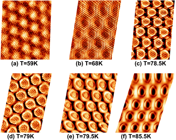 | ||
| Fig. 1 STM image sequence of xenon desorption from the nanomesh. Scale: pore–pore distance = 3.2 nm, sample bias (US) = −320 mV, IT = 0.5 nA. (a) Xe multilayer at T = 59 K, (b) Xe monlayer at T = 68 K, (c) Partial Xe desorption from wires at T = 78.5 K, (d) Wires completely Xe free at T = 79 K, (e) A few Xe atoms in the center of the pores at T = 79.5 K, (f) Xe “rings” at the rims of the pores at T = 85.5 K. | ||
A further increase of the temperature above 73 K leads to a slightly enhanced mobility of the Xe atoms in the pores.
At 78.5 K, Xe atoms at the intersection of the wires are desorbed (Fig. 1c), which leads to an enhanced imaging of the nanomesh pore structure, where the Xe atoms at the rim of the pores appear brighter and the ones at the bridge sites between the pores are still adsorbed. The Xe is still in a ( )R30° configuration with an average number of 25 ± 3 Xe atoms in the pore. Slightly increasing the temperature by 0.5 K leads to the desorption of Xe from such bridge sites, and Xe is now only present in the pores of the nanomesh, as shown in Fig. 1d. The (
 )R30° structure of the Xe is still is prevailing, but the mobility is further enhanced in some pores and the Xe appears less well ordered in the image. By heating the sample further to 79.5 K, more Xe is desorbed and the mobility of the remaining Xe is increased and only the residence probability but not the true atomic positions can be revealed. The wires and the rims of the pores show the atomic resolution of the clean h-BN nanomesh and the Xe atoms appear to cluster in the center of the pores, with a quasi amorphous structure. Between 80 K and 86 K a significant change in the residence probability of the Xe is observed resulting in the appearance of the nanomesh as shown in Fig. 1f. The pores and wires could be clearly distinguished with atomic resolution on the clean wires as already observed at 79.5 K. But now a homogenous ring at the rim of the pore can be observed instead of a cluster in the center of the pore. The ring has a mean diameter of 1.5(2) nm and a width of 0.55(10) nm. Such rings are only observed during the Xe desorption experiments and we attribute them to mobile Xe atoms moving in the pore with the highest residence time at the pore rim. In this sense the width of the ring represents a convolution of the residence probability and the STM tip and is therefore expected to be larger than 0.432 nm, the van der Waals radius of Xe. This view will be reinforced by the MD simulations, the noise analysis of the STM images and the measurement of stable rings at low temperatures. These Xe rings have been predicted recently9 and are visualized now for the first time showing dynamics in accordance with MD simulations at elevated temperatures as we will show here below.
In order to confirm the presence of Xe rings in a static configuration a submonolayer coverage of Xe on the nanomesh was deposited and imaged at 5 K. Fig. 2a shows a large-scale STM image with a coverage of ∼1/3 ML where a few Xe rings in the pores, filled pores and empty pores are discernable. The step edges remain undecorated outside the pore regions. Fig. 2b shows a high-resolution STM image where single Xe atoms are clearly discernible. One can see that Xe preferentially fills the pores completely by hexagonal islands adopting a ( )R30° structure as in the monolayer at higher temperatures. The average number of Xe atoms in the pores is 24 Xe (ranging from 23 to 29), which is in good agreement to the case at 78.5 K and 79 K (Fig. 1c and d). The rings are now much better defined than in the high temperature case with a width of 0.45(5) nm which is now closer to the van der Waals diameter of the Xe. The rings show structure around the circumference with typically 12 Xe atoms that can be distinguished. As can be seen from the ring in Fig. 2b, the Xe atoms sometimes seem to form dimers, which are imaged as elongated features rather than two clearly discernible spherical protrusions. The number of 12 Xe rim atoms was predicted in ref. 9.
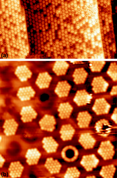 | ||
| Fig. 2 STM images of submonolayer xenon on a nanomesh at 5 K (a) 100 × 50 nm2, US = 1 V, IT = 100 pA, (b) 17 × 17 nm2, US = 250 mV, IT = 50 pA. | ||
Summarizing these results, three main findings can be extracted: (i) the selectivity of the pores with respect to the wires, (ii) the clear preference of the Xe 2D adsorbate for a ( )R30° phase and (iii) the appearance of Xe rings at the rim of the pores. In order to explain the origin of such complex behavior, not only must the nanomesh “large scale” corrugation of the adsorption potential be taken in account, but also the atomistic nanomesh structure which dictates the substrate potential competing with the lateral Xe–Xe interactions for the determination of the adsorbate ordering.
The system was therefore modeled using classical MD of Xe adsorbates in contact with a periodic, rigid substrate consisting of 1 ML h-BN on three atomic layers of Rh(111) in the optimal nanomesh configuration as computed by density functional theory (DFT) calculations.13 For the Xe–Xe interactions, we resorted to the best potential function available12 particularly suitable for the condensed phases. Concerning the Xe–substrate interaction we employed a Lennard-Jones potential with standard parameters available in literature15,16 using the usual combination rules to determine the interaction parameters of Xe with B, N, and Rh. We call this potential V{S1}. We do not include classical electrostatics terms, since we have no access to the charge distribution that could be obtained by a full ab initio calculation. Instead, we decided to modify the strength of the pairwise potential between Xe and the atoms of the substrate, in order to reproduce the important features of the experiments. In the following, V{S2} will refer to the modified Xe–substrate potential. We will show that the modification of the pairwise potential can be regarded as an implicit inclusion of the polarization component in the interaction between the Xe and the substrate.
A most successful reproduction of the experimentally observed Xe adsorption behavior has been achieved by arbitrarily doubling the strength of the pairwise Xe–substrate interaction in the corresponding simulation. To explain this approach we have estimated the polarization contribution of the surface potential to the Xe adsorption by finite element (FE) simulations of the electrostatic potential Φ(r) above the nanomesh. These simulations are based on the surface potential differences between pores and wires reported in ref. 9 and the assumption that the contribution to the Xe adsorption is purely of polarization type, i.e.
![[hair space]](https://www.rsc.org/images/entities/char_200a.gif) e−39 C m2 V−1. Details of the electric potential simulation are given in the ESI.† A comparison of the polarization contribution with the unmodified pairwise potential V{S1} is shown in Fig. 3.
e−39 C m2 V−1. Details of the electric potential simulation are given in the ESI.† A comparison of the polarization contribution with the unmodified pairwise potential V{S1} is shown in Fig. 3.
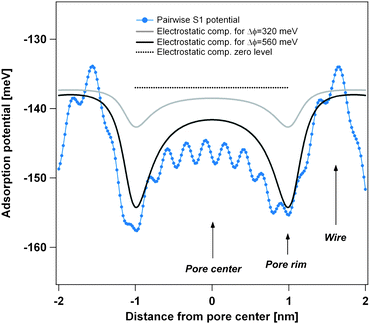 | ||
| Fig. 3 Comparison of the theoretical pairwise Xe–substrate potential V{S1} with the polarization contribution for an assumed surface potential difference between pore and wires. The light grey curve assumes a surface potential difference of 320 meV as measured by photoemission spectroscopy of adsorbed xenon (PAX)9 and the black curve a surface potential difference of 560 meV as obtained from DFT calculations.9 Both curves of the polarization contribution are vertically off-set by −137 meV for better comparison. | ||
One can see that the shape of the V{S1} potential and the polarization contribution is very similar and for the theoretically predicted ΔΦ = 560 meV surface potential difference between pore and wires, the magnitude is nearly the same. Therefore the polarization contribution can be well represented in the pairwise potential by doubling its strength, which we have done in going from V{S1} to V{S2}. It should be noted, however, that the polarization contribution does not lead to significant adsorption energy on the wires or in the pores (polarization related curves in Fig. 3 are vertically offset by −137 meV). Therefore, the doubling of the pairwise potential will lead to a relative corrugation of the adsorption potential which faithfully combines the van der Waals and the polarization contribution. The absolute adsorption energy is however overestimated by a factor of nearly 2, which doesn't influence the simulation, as desorption is not included.
In a first step a single Xe atom sampling the potential energy surface (PES) is moved on a grid parallel to the substrate. For each lateral position of a single Xe atom, its minimum with respect to the direction orthogonal to the surface is determined with a different substrate potential strength.
In Fig. 4, the PES for the potential V{S2} is shown, which is found to be more reliable when comparing to experimental data (see Fig. S1 of the ESI†). As it can be seen from Fig. 4a, the corrugation between the bottom of the pore and the wires is less than 100 pm, whereas Fig. 4b shows that the binding energy of a single Xe atom appears too large (290 meV at the bottom of the pore) with respect to similar systems.17 However, this strength, as we will show below, allows reproducing in an effective way most of the experimental results, showing that some of the effects neglected by this model based on simple pairwise interactions, in particular of polarization nature arising from surface potential differences, can be reproduced by an enhanced effective interaction of the Xe atoms with the substrate. It is worth noting that the absolute minimum appears at the rim of the pore, with a minimum depth of about 20 meV. Although 12-membered rings could not be stabilized during our MD simulations (close-packed islands were always favored), this PES profile is encouraging and appears in agreement with the experimentally observed rings at low coverage (Fig. 2).
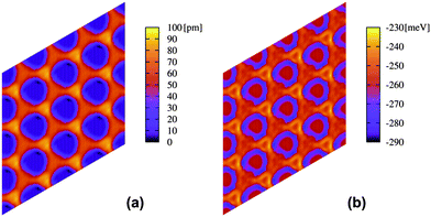 | ||
| Fig. 4 (a) Height profile in picometres and (b) energy profile in meV for a single Xe atom on the nanomesh and potential V{S2}. Scale: pore–pore distance = 3.2 nm. | ||
In order to understand the interplay between pore selectivity, ring formation and stability of commensurate phases, a series of MD simulations at various Xe coverages was performed.
To this end, we validate the results obtained using the V{S2} potential towards the experimentally observed structures.
For the full Xe monolayer coverage, different orientations with respect to the substrate were investigated. Two local minima were found at 0° and 30° rotation angles of the Xe [10] lattice direction with respect to the [10] direction of the h-BN layer, where with our V{S2} potential the experimentally observed 30° rotation is found to be favorable by about 20 meV per Xe atom. Moreover, the optimal density of Xe is found to be (55 ± 1) Xe atoms per nanomesh unit cell, which corresponds well with the experimentally observed density for the ( )R30° structure (Fig. 1b).
To investigate intermediate Xe coverages a series of annealing cycles at high temperature, each with different coverage, was performed. Desorption is not included in this model, which would require grand canonical Monte Carlo simulations. Nevertheless, important structural properties can be inferred using this procedure. All the MD simulations presented here are run in a supercell containing 16 pores, with periodic boundary conditions in the lateral directions.
The protocol to obtain structural minima for a certain coverage consisted of annealing at high temperature, followed by a gradual cooling of the system. Starting with an initial configuration with all Xe atoms in the wires, substrate potential V{S2} confines the adsorbate mostly in the pores and keeps all of them oriented in islands with the ( )R30° structure, whereas this selectivity is not observed for the potential V{S1} (see the ESI†).
After this preliminary test, it can be concluded that our protocol is unbiased enough (since the memory of the wires population is lost) and that the potential V{S2} can be used for the subsequent simulations.
These simulations were performed again with different series of coverages ranging from 0.12 to 0.56. Higher coverages can not be reproduced faithfully by our strategy, since the desorption from the wires, not included in canonical MD simulations because of relatively high desorption barriers with respect to simulation times, should play a major role in such cases.
After annealing and subsequent cooling, the number of atoms in pores and wires were plotted as a function of the coverage (see the ESI†). We note that the number of atoms per pore in the filled pores (with more than 8 Xe atoms) remains above 20 for all coverages larger than 0.4. Moreover, for coverages smaller than 0.5 the number of atoms in the wires substantially decreases. Additionally, the number of islands that show the rotated orientation as in the experiment is always prevalent, and as soon as the coverage exceeds 0.5, nearly all domains are oriented as in the experiment. As an example, the final configuration for the coverage of 0.27 and for the coverage of 0.75 is shown in Fig. 5.
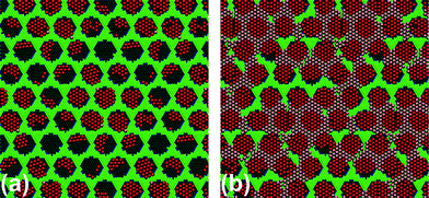 | ||
| Fig. 5 Final configuration for coverages (a) 0.27 and (b) 0.75 (the unit cell is made by 16 pores). Xe atoms in the pores are highlighted in red. Almost all Xe islands in the pores are rotated by 30 degrees as prevalent in the experiment. | ||
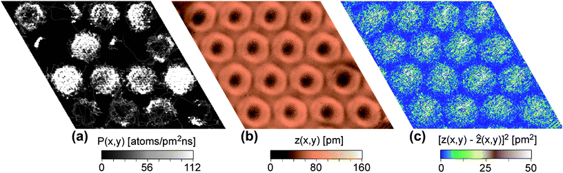 | ||
| Fig. 6 Analysis of the Xe residence probability: (a) Permanence statistics for a simulation at T = 95 K with the potential V{S2} (see text). The pores with at least 3 Xe atoms and fewer than 8 atoms show a ring-like shape denoting a dynamic preference for the permanence on the rim of the pore. (b) STM image with Xe “rings” at the rims of the pores at T = 85.5 K according to Fig. 1f, US = 1 V, IT = 1 nA. (c) Noise analysis derived from STM image in (b). | ||
Our simulations did not reveal the formation of static Xe rings as observed at 5 K. However, the experimentally observed static Xe rings as shown in Fig. 2 are present only in about 4% of the pores, whereas 80% of the pores are filled by hexagonal islands similar to the ones of the simulation. The Xe rings in the experiments become the dominant feature only at high temperature and are dynamic, not static. It should be noted that during our MD simulations, dynamic motion of Xe rings along the step rim was observed. In Fig. 6, an analysis of the Xe residence probability on the nanomesh is shown, where Fig. 6a represents the calculated permanence statistics at high temperature (95 K) along a 1 nanosecond trajectory for a sample with an average number of 8 Xe atoms per pore. Brighter zones in this permanence statistics analysis correspond to higher population. When the number of Xe atoms in the pore is neither too small (the rim is not sampled completely in this simulation time), nor too big (the whole pore is sampled), one can see that ring-like features appear comparable to the experimental results displayed in Fig. 2. Note that the ring-like structure appears already with 3–4 Xe atoms in the pores, whereas (due to our potential V{S2}) compact structures are favored already with 7–8 atoms in the pore. This argumentation is supported by the noise analysis displayed in Fig. 6c derived from an experimental STM image (Fig. 6b). In the case of mobile adsorbents the topographic height measured in the STM can be related to the local resident probability of the adsorbent.18 This relation is rather complex as it depends on the tunneling conditions and STM feedback loop parameters. However, the transient nature of Xe atoms moving under the tip is reflected in the noise of the STM topographic signal. In Fig. 6b the ring like features around the pores are easily observed. The noise amplitude of the topographic signal is displayed in Fig. 6c and one can see that on the wires (especially the wire junctions) the noise is very low. This indicates that indeed the topographic image is dominated by the dynamics of the Xe and that the Xe has low residence and transient probability in the wire region. On the other hand, the noise level in the pore regions is high with a maximum toward the pore center. This indicates that the Xe is not moving exclusively around the pore rim, but there are also transient passages through the pore centers, however with a lower residence probability (lower STM topography). This behavior is well reproduced by the simulation of Fig. 6a.
4. Conclusions
We have investigated the temperature-dependent difference in the site-specific Xe adsorption on h-BN on a Rh(111) nanomesh. In combination with MD simulations the STM investigations reveal the adsorption energy landscape of this remarkable nanotemplate substrate, which has a pronounced adsorption energy maximum on the rim of the nanomesh pore. Experimentally as well as theoretically, we could directly demonstrate the existence of Xe rings in this rim maximum of the adsorption energy. Dependent on the substrate temperature the Xe atoms can be mobile in these rings or at 5 K can be frozen into static rings of 12 Xe atoms.We have shown that the adsorption behaviour can not be understood by looking at the van der Waals or electrostatic polarization interaction individually. Both effects contribute in a similar magnitude to the lateral variation of the adsorption potential landscape and therefore to the site specificity. However, regarding the absolute magnitude, the van der Waals contribution largely dominates the adsorption energy.
The Xe rings on the h-BN nanomesh surface reminds us of the quantum corrals by Eigler et al.,19 which had to be built atom-by-atom. The template effect of the nanomesh provides a physical basis to form self-assembled arrays of units with functionalities on this single-layer dielectric template surface. This effect in the formation of ordered arrays could probably be generalized and also be confirmed in other nanostructures.
Acknowledgements
Financial support by the Empa research commission (No. 880138) and by the Swiss National Foundation (No. 122703) is gratefully acknowledged. HS acknowledges financial support from the European Union (No. NMP4-CT-2004-013817). The authors also thank T. Greber (University of Zürich) and Abdelkader Kara (University of Central Florida) for fruitful discussions.References
- J. Barth, Annu. Rev. Phys. Chem., 2007, 58, 375 CrossRef CAS.
- (a) W. Xiao, P. Ruffieux, K. Aït-Mansour, O. Gröning, K. Palotas, W. A. Hofer, P. Gröning and R. Fasel., J. Phys. Chem. B, 2006, 110, 21394 CrossRef CAS; (b) J. Barth, H. Brune, G. Ertl and R. J. Behm, Phys. Rev. B: Condens. Matter, 1990, 42, 9307 CrossRef CAS; H. Brune, H. Röder, C. Boragno and K. Kern, Phys. Rev. B: Condens. Matter, 1994, 49, 2997 CrossRef CAS; (c) K. Aït-Mansour, P. Ruffieux, W. Xiao, P. Gröning, F. Fasel and O. Gröning, Phys. Rev. B: Condens. Matter Mater. Phys., 2006, 74, 195418 CrossRef.
- S. Rousset, V. Repain, G. Baudot, Y. Garreau and J. Lecoeur, J. Phys.: Condens. Matter, 2003, 15, S3363 CrossRef CAS.
- F. Silly, M. Pivetta, M. Ternes, F. Patthey, J. P. Pelz and W. D. Schneider, Phys. Rev. Lett., 2004, 92, 016101 CrossRef.
- (a) M. Nonnenmacher, M. P. O'Boyle and H. K. Wickramasinghe, Appl. Phys. Lett., 1991, 58, 2921 CrossRef; (b) P. Ruffieux, K. Ait-Mansour, A. Bendounan, R. Fasel, L. Patthey, P. Gröning and O. Gröning, Phys. Rev. Lett., 2009, 102, 086807 CrossRef CAS.
- N. D. Lang and W. Kohn, Phys. Rev. B: Solid State, 1970, 1, 4555 CrossRef; D. E. Beck, Solid State Commun., 1984, 49, 381 CrossRef CAS.
- R. Smoluchowski, Phys. Rev., 1941, 60, 661 CrossRef CAS.
- S. Berner, M. Corso, R. Widmer, O. Groening, R. Laskowski, P. Blaha, K. Schwarz, A. Goriachko, H. Over, S. Gsell, M. Schreck, H. Sachdev, T. Greber and J. Osterwalder, Angew. Chem., Int. Ed., 2007, 46, 5115 CrossRef CAS.
- H. Dil, J. Lobo-Checa, R. Laskowski, P. Blaha, S. Berner, J. Osterwalder and T. Greber, Science, 2008, 319, 1824 CrossRef CAS.
- H. Sachdev, to be published.
- I. Horcas, R. Fernández, J. M. Gómez-Rodríguez and J. Colchero, Rev. Sci. Instrum., 2007, 78, 013705 CrossRef CAS.
- R. A. Aziz and M. J. Slaman, Mol. Phys., 1986, 57, 825 CAS.
- R. Laskowski and P. Blaha, J. Phys.: Condens. Matter, 2008, 20, 064207 CrossRef.
- M. Dunin von Przychowski, H. Wiechert, G. K. L. Marx and G. Schönhense, Surf. Sci., 2003, 541, 46 CrossRef CAS.
- A. D. Migone, M. T. Alkhafaji, C. Vidali and M. Karimi, Phys. Rev. B: Condens. Matter, 1993, 47, 6685 CrossRef CAS.
- C. Schwartz and R. J. Le Roy, Surf. Sci., 1986, 166, L141 CrossRef CAS.
- J. Küppers, K. Wandelt and G. Ertl, Phys. Rev. Lett., 1979, 43, 928 CrossRef.
- J. A. Stroscio and R. J. Celotta, Science, 2004, 306, 242 CrossRef CAS.
- E. J. Heller, M. F. Crommie, C. P. Lutz and D. M. Eigler, Nature, 1994, 369, 464 CrossRef.
Footnote |
| † Electronic supplementary information (ESI) available: Simulation details and Figs. S1–S6. See DOI: 10.1039/b9nr00431a |
| This journal is © The Royal Society of Chemistry 2010 |