Upscaling of polymer solar cell fabrication using full roll-to-roll processing
Frederik C.
Krebs
*,
Thomas
Tromholt
and
Mikkel
Jørgensen
Risø National Laboratory for Sustainable Energy, Technical University of Denmark, Frederiksborgvej 399, DK-4000 Roskilde, Denmark. E-mail: frkr@risoe.dtu.dk
First published on 4th May 2010
Abstract
Upscaling of the manufacture of polymer solar cells is detailed with emphasis on cost analysis and practical approach. The device modules were prepared using both slot-die coating and screen printing the active layers in the form of stripes that were serially connected. The stripe width was varied and the resultant performance analysed. Wider stripes give access to higher geometric fill factors and lower aperture loss while they also present larger sheet resistive losses. An optimum was found through preparation of serially connected stripes having widths of 9, 13 and 18 mm with nominal geometric fill factors (excluding bus bars) of 50, 67 and 75% respectively. In addition modules with lengths of 6, 10, 20, 22.5 and 25 cm were explored. The devices were prepared by full roll-to-roll solution processing in a web width of 305 mm and roll lengths of up to 200 m. The devices were encapsulated with a barrier material in a full roll-to-roll process using standard adhesives giving the devices excellent stability during storage and operation. The total area of processed polymer solar cell was around 60 m2 per run. The solar cells were characterised using a roll-to-roll system comprising a solar simulator and an IV-curve tracer. After characterisation the solar cell modules were cut into sheets using a sheeting machine and contacted using button contacts applied by crimping. Based on this a detailed cost analysis was made showing that it is possible to prepare complete and contacted polymer solar cell modules on this scale at an area cost of 89 € m−2 and an electricity cost of 8.1 € Wp−1. The cost analysis was separated into the manufacturing cost, materials cost and also the capital investment required for setting up a complete production plant on this scale. Even though the cost in € Wp−1 is comparable to the cost for electricity using existing technologies the levelized cost of electricity (LCOE) is expected to be significantly higher than the existing technologies due to the inferior operational lifetime. The presented devices are thus competitive for consumer electronics but ill-suited for on-grid electricity production in their current form.
 Frederik C. Krebs | Frederik Christian Krebs received his PhD from the Technical University of Denmark in year 2000 and has since then worked in the field of polymer solar cells at Risø National Laboratory for Sustainable Energy. He is currently professor at Risø DTU within areas of research that include new materials with low bandgaps and novel processing capability, large-area processing and manufacture of polymer solar cells, stability and lifetime testing, degradation mechanism studies, outside testing and demonstration. |
 Thomas Tromholt | Thomas Tromholt received his MSc in Nanotechnology in 2009 from Aalborg University, Denmark. He is currently pursuing a PhD with a focus on material characterization of organic photovoltaics at Risø National Laboratory for Sustainable Energy. |
 Mikkel Jørgensen | Mikkel Jørgensen received his MSc in Chemistry from the University of Copenhagen and his PhD in Organic Chemistry from the University of Copenhagen (1990). He worked as an industrial chemist at NycoMed (1987–1990) during his PhD studies and later as an industrial Chemist at PNA Diagnostics (1990–1993). He then became employed as a senior Scientist at Risø National Laboratory, DTU, Denmark (1994–present). His scientific interests include synthetic chemistry, NMR, chemistry of materials, carrier mobilities in organic materials, energy levels and energy level alignment in organic materials by UPS studies, solar cells, polymers, fluorine chemistry and supramolecular chemistry. |
1. Introduction
Polymer solar cells1–8 are a photovoltaic technology where the active layer is thin and can be applied at low temperature from solution. Since this mode of preparation allows for both high speed and low cost the view held by many is that polymer solar cells are the first example of a photovoltaic technology that truly solves the problem of high cost and low throughput speed that all other photovoltaic technologies are faced with. It should however also be highlighted that while many critics agree with the above they also view polymer solar cells as a technology with some problems for which no immediate solution exist in spite of a relatively intense research effort over the past 10 years. The performance9–11 and especially the lifetime4,12–18 of polymer solar cells need to see significant developments before polymer solar cells will be competitive for production of on-grid electrical energy. The current stage of development is however well suited for demonstrations19 and niche products where the polymer solar cell acts as a discrete power source for low-energy electronic applications and stand-alone systems e.g. in conjunction with a rechargeable battery. An additional point that is often raised by critics is that polymer solar cells do not exist outside the laboratory while they are compared with existing and well proven photovoltaic technologies that are manufactured industrially. It is clear that the comparison of laboratory cells for an emerging technology with commercially available solar cells is not balanced, especially because very few of the polymer solar cell claims have been verified. This point is also underlined by the fact that polymer solar cells are often presented as a low-cost solution processed technology while being prepared on rigid glass substrates by often complex and cumbersome processes such as slow drying of the active layer and vacuum deposition of electrodes (e.g. indium tin oxide, aluminium). Finally, the results presented are most often the best results and not the average that would represent the capacity of the technology better. It is thus understandable why critics find great difficulty in agreeing that polymer solar cells should be a commercially and environmentally viable technology. A good argument in support of the view of the critics is that the field of polymer solar cells has not yet answered the question: if polymer solar cells have such a great potential why are they not here yet? When viewing the scene from above it is clear that polymer solar cells need to see a lot of development to meet the strongholds of the critics. There have however been remarkable improvements recently in the areas of power conversion efficiency,9–11 stability,12–17 processing in large areas,19–23 the alleviation of indium tin oxide,22–24 demonstrations19 and organic photovoltaics (OPV) became commercially available from Konarka in 2009. In addition, polymer solar cell modules have been available to the public19 and scientific groups have started sharing cells and performing round robins.25 With these developments in mind there is still a strong hope that polymer solar cells will be able to answer the views held by their critics.The purpose of this work was to upscale the manufacture of polymer solar cells from the laboratory level to an industrial level and identify the instruments requirements for complete polymer solar cell module manufacture and describe a complete process enabling manufacture of electrically contacted and characterised polymer solar cell modules that are ready to be implemented in electronic applications. A complete cost analysis detailing processing speed, manual labour and materials cost was also sought so that it is possible to estimate the manufacturing and electricity cost correctly. Finally the capital investment in machinery for the process is detailed.
2. Experimental techniques
2.1 Materials
P3HT was purchased from BASF (Sepiolid P200) or prepared at Risø DTU in batches of approximately 40 g. [60]PCBM and [fullerene]PCBM were purchased from Solenne B.V. the PCBM based on a mixture of fullerenes was lower in cost and found to perform identically to purified [60]PCBM in the experiments carried out here. ZnO nanoparticles were prepared by caustic hydrolysis of Zn(OAc)2·2H2O as described previously19–21 and was used for ink formulations using both WS-126,27 and acetone as solvents. In both cases the ink was stabilized with MEA (methoxy-ethoxy-acetic acid) and filtered through a 0.45 micron filter before coating. The ink for the active layer was prepared by dissolving P3HT (18–24 mg mL−1) and the PCBM (16–22 mg mL−1) in half the final volume of 1,2-dichlorobenzene at 120 °C for 3 h followed by addition of the second half of the final volume of chloroform. The ratio between P3HT and PCBM was typically 10![[thin space (1/6-em)]](https://www.rsc.org/images/entities/char_2009.gif) :9. PEDOT:PSS was purchased as EL-P 5010 from Agfa and was diluted slowly with isopropanol using stirring until a viscosity of 270 mPa s was obtained. The silver inks employed were all screen printable and either heat or UV-curable (see Table 1). The adhesive for encapsulation was 467 MPF from 3M and the barrier material was purchased from Alcan.25
:9. PEDOT:PSS was purchased as EL-P 5010 from Agfa and was diluted slowly with isopropanol using stirring until a viscosity of 270 mPa s was obtained. The silver inks employed were all screen printable and either heat or UV-curable (see Table 1). The adhesive for encapsulation was 467 MPF from 3M and the barrier material was purchased from Alcan.25
| Silver Ink | Max PCE (%) | Mean PCE (%) | Mean Isc/mA | Mean Voc/V | Mean FF (%) |
|---|---|---|---|---|---|
| Toyo UV | 2.20 | 1.95 (±0.19) | 61.8 (±2.4) | 7.75 (±0.30) | 39.0 (±2.0) |
| Toyo Solvent | 0.77 | 0.65 (±0.08) | 40.7 (±5.8) | 5.38 (±0.46) | 28.6 (±1.5) |
| Spraylat XCMS-016 | 1.00 | 0.86 (±0.09) | 44.8 (±2.5) | 6.12 (±2.5) | 30.1 (±1.1) |
| Spraylat XCMD-022 | 0.83 | 1.05 (±0.07) | 44.8 (±2.4) | 6.87 (±0.39) | 32.7 (±1.2) |
| Spraylat XCMS-031 | 1.17 | 1.11 (±0.10) | 53.7 (±2.7) | 6.23 (±0.21) | 31.9 (±1.0) |
| Dupont 410 | 1.73 | 1.64 (±0.05) | 54.7 (±1.2) | 7.78 (±0.07) | 37.1 (±0.8) |
| Spraylat XPVS-145 | 0.70 | 0.60 (±0.07) | 41.0 (±4.5) | 4.77 (±0.35) | 29.8 (±1.2) |
| Dupont 5000 | 1.01 | 0.96 (±0.03) | 40.6 (±3.9) | 7.18 (±0.4) | 31.8 (±0.96) |
| Dupont 5007E | 1.29 | 1.13 (±0.10) | 52.2 (±3.5) | 6.53 (±0.25) | 31.9 (±1.32) |
| Dupont 5025 | 1.59 | 0.93 (±0.44) | 45.6 (±8.5) | 5.96 (±1.77) | 31.7 (±3.0) |
2.2 Device geometry
Light has to be able access the active layer of the solar cell and this implies that one of the electrodes should be transparent. The most commonly employed transparent conductor is indium tin oxide (ITO) which is available on flexible PET foils. In this case 130 micron PET was employed with a fully covering 60 Ω square−1 layer of ITO that had been sputtered on one side in a vacuum roll-to-roll process. Due to the relatively high sheet resistivity of the ITO it is necessary to pattern the ITO such that smaller cells can be connected in series. In this way Ohmic losses are reduced at the expense of the total active area. Fig. 1 shows the principle whereby the ITO is patterned into stripes that are then serially connected via the ensuing printing processes. The serial connection is achieved in the final printing step.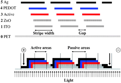 | ||
| Fig. 1 The substrate (PET) is shown along with the position and order of the layers. ITO (1), ZnO (2), Active (3), PEDOT (4) and silver (5). The view is along the striped pattern (above). The finally connected module is shown schematically (below) as three serially connected stripes where the active areas and passive areas are highlighted. | ||
In principle the striped pattern could be endless but we chose to pattern the ITO in stripes that extend for the length of the typical module as shown in Fig. 2. Register and cutting marks were printed along the web along with lock holes that enable registration and juxtaposition of subsequent layers with respect to the first ITO layer during later printing and for the final cutting of the modules. The lengths of the stripes were 200, 225 and 250 mm (shown for 225 mm in Fig. 2).
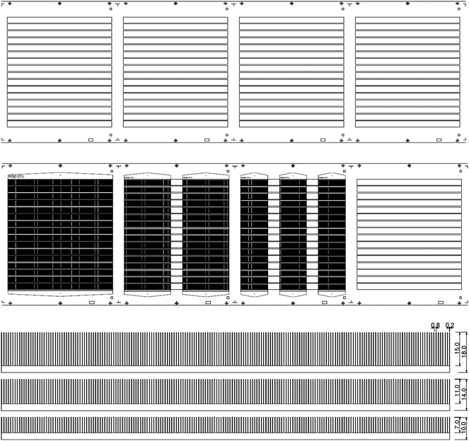 | ||
| Fig. 2 The substrate (PET) is shown with the etched ITO pattern and register marks. The 16 ITO stripes each measure 225 × 13 mm and are spaced along the web direction by 25 mm (top). The silver print for three of the different module lengths are shown overlaid on the ITO pattern (middle). The 225 mm long modules (middle left), 100 mm long modules (middle center) and 60 mm long module (middle right) are shown. The printed silver pattern is shown for the modules with 9, 13 and 18 mm wide ITO (bottom). | ||
In the case of the modules that were shorter than the ITO length in the direction of the web those were printed so that they overlapped with the ITO but maintained a repetition gap of 25 mm in order to enable cutting.
2.3 Roll-to-roll slot-die coating
A system comprising un-winder, corona treater, edge guide, web cleaning, discharge rods, coating roller, ink-jet labelling printer, dryer, cooling roller and re-winder was employed.20 The web tension was typically 80–90 N during all experiments. It was found necessary to clean the ITO substrate by passage through the system using corona treatment (1070 W), web cleaning and washing using isopropanol followed by drying at 140 °C. Each motif was labelled on the back side with the date and a unique number for later identification. The layers were slot-die coated using a modified procedure described earlier.20,21The drying temperature in all experiments was 140 °C. The ZnO solution was slot-die coated at a speed of 2 m min−1 with a wet layer thickness of 3.125 micron and a dry layer thickness of 23 nm. The active layer was coated at a speed of 1.4 m min−1 with a wet layer thickness of 4.85 micron and a dry layer thickness of 127 nm and the PEDOT:PSS was coated at a speed of 0.3 m min−1 with a wet layer thickness of 75 μm and a dry layer thickness of 20 μm (Fig. 3). The slow web speed during coating PEDOT:PSS is due to the short available drying length of 1 m. To ensure proper drying of the thick PEDOT:PSS layer only slow speeds could be employed.
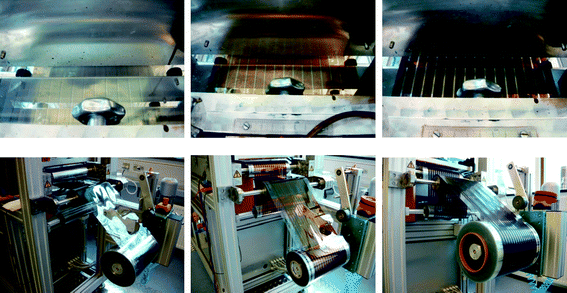 | ||
| Fig. 3 The slot-die coating of ZnO nanoparticles (left), P3HT:PCBM (middle) and PEDOT:PSS (right). The wet films are shown above and the corresponding dried films are shown below. | ||
2.4 Roll-to-roll screen printing
Two different screen printing systems were employed. The first system was a Klemm line employed for printing a UV-curable etch resist on top of the raw PET-ITO foil with the desired ITO pattern while also punching a registry hole along the edge of the foil for each printed motif. This hole was used for later registration while printing of the back electrode. This system comprised an un-winder, flat bed screen printer, UV-curing oven, and re-winder. The system was operated at 800 prints hour−1 corresponding to a web speed of 3.3 m min−1. The ITO was then etched using CuCl2(aq) followed by washing, stripping of the etch resist and drying. The processing speed during etching, stripping and drying of the ITO was 180 m hour−1 corresponding to a web speed of 3 m min−1. The screen printing of the silver back electrode was carried out on a flat bed roll-to-roll screen printer from Alraun comprising un-winder, metering wheel, positioning camera, vacuum table, screen printer (AT701), hot air oven, transport rollers, dancing tensioning roller and re-winder. The positioning followed a hole that was punched during screen printing of the etch resist for the ITO (vide infra). The system is fully automated and controlled by a computer. The positioning of the module on the vacuum table is achieved using register marks printed during screen printing of the silver layer. The foil was moved forward at a speed of 1 m min−1 until the register mark was reached. The foil was then fixed on the vacuum table and the motif was printed followed by moving the foil to the next motif. The effective web speed was 1 m min−1 which is intentionally low due to the relatively short drying length for the oven (120 cm). The residence time in the oven was 72 s and the drying temperature was 130 °C. A photograph of the screen printing is shown in Fig. 4.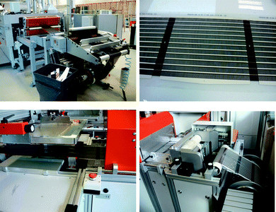 | ||
| Fig. 4 Screen printing of silver using a Klemm line as seen from the un-winder (top left) and the same device type (12 × 18 mm stripes) after having printed the silver (top right). Flat bed screen printing using a flat bed screen printer from Alraun (bottom left) showing 16 × 13 mm stripes on the re-winder (bottom right). | ||
2.5 Roll-to-roll lamination
Complete lamination of the modules was carried out in several steps that all employed the laminator shown in Fig. 5. Firstly the adhesive was laminated onto the barrier foil. The width of the barrier foil was 305 mm while the width of the lined adhesive (3M 467 MPF) was 298 mm to avoid adhesive build-up on the laminating rubber rollers in case of slight misalignment between adhesive and barrier foil. The barrier material with the lined adhesive could then be cut to a width of 250 mm for the back side in order to enable lamination of the active areas while exposing some of the silver bus bars for electrical connections during roll-to-roll IV testing.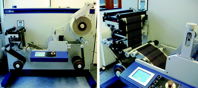 | ||
| Fig. 5 Laminator comprising un-winder, edge guide and cutting table, laminator, laminate un-winder, longitudinal cutting knifes and re-winder (left). A photograph of the edge guide system (right). | ||
After application of the adhesive onto the barrier foil it was laminated onto the un-encapsulated solar cell material. Typically the lamination was first carried out on the back side of the device to avoid excess handling of the sensitive active layers in the device. In the final step barrier material was laminated onto the front side of the device.
2.6 Roll-to-roll IV characterisation
IV characterisation was carried out on a modified roll-to-roll system from Alraun comprising un-winder, positioning camera, vacuum table with connections, pneumatic contacting pads, solar simulator, video camera, transport rollers, dancing tensioning roller and re-winder. The system is fully automated and controlled by a computer. The positioning of the module on the vacuum table is achieved using register marks printed during screen printing of the silver layer.Once the module to be tested has been positioned vacuum is applied to the vacuum table to fix the module over the contacts. Contact is made by pneumatic cylinders that force contact between a conducting strip on the vacuum table and the device. It is possible to employ both top and bottom contacting schemes in the system. The IV measurements are then carried out using a Keithley 2400 sourcemeter. The computer program allows for tracing multiple curves, annealing the device and a set of criteria can be set determining when the next module should be tested. For each device a report is generated in Excel format including the data which may include the latest IV curve, a photograph of the device and annealing behaviour of Isc, Voc, FF, PCE, Rs and Rsh as a function of time. In addition, a summary report for the entire roll is generated. This enables the quick identification of devices on the roll that behaves abnormally. A schematic drawing and a photograph of the roll-to-roll IV tester is shown in Fig. 6. The lamp source is a Steuernagel KHS1200 providing approximately AM 1.5 G and 1000 W m−2 at the position of the solar cell module. The temperature of the devices during testing is 72 °C. The typical scheme for characterisation when aiming at carefully establishing that the device exhibits the desired operational stability was to record IV curves continuously from −20 to +20 V for a set period of time (2–20 min) and continue to the testing of the next module unless the change in performance (dPCE/dt) was larger than 0.01%. After completion of the testing the data was carefully analysed (vide supra).
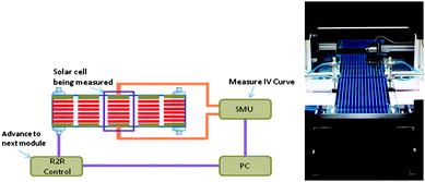 | ||
| Fig. 6 The roll-to-roll IV tester is shown schematically (left). The setup consists of a roll-to-roll system (Alraun) that can be controlled via a PC through a custom made hardware control (R2R Control). Solar cell modules are automatically positioned under an AM 1.5 sun simulator (Steurnagel LichtTechnik). Pneumatic actuators (not shown) bring the solar cell in contact with leads running to an SMU that performs IV scans. In annealing mode IV scans are repeated until a stable PCE is reached and the software then instructs the R2R control to advance the roll to the next module. A photograph along the roll of solar cells is shown from the un-winding side (right). The metering wheel and positioning camera can be seen in the upper part of the image and the pneumatic contacting cylinders can be seen under the solar simulator in the middle of the image. | ||
2.7 Sheeting
The sheeting of the solar cells was carried out using a knife cutting tool mounted on a machine with an unwinding unit and a forward roller controlled by a camera that triggers the knife when a registry mark is passing. The system then stops transporting the foil, cuts and transports the foil again until the next registry mark is reached. The sheeted solar cells are conveyed on a belt where they can be collected in bunches and packed. The machine is shown in Fig. 7. It should be noted that cutting through ITO is not always so easy and for the larger modules that made use of the full ITO motif this was not a problem as the cut was made through PET only. In case of the modules where there were 2 or 3 printed silver modules per ITO motif two of the cuts were made through the ITO and this often lead to slight delamination close to the cut (2–3 mm). This could possibly be avoided by the use of a laser cutting machine.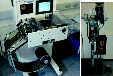 | ||
| Fig. 7 The simple sheeting machine employed in this study comprising un-winder, transport roller camera, knife cutter and conveyor belt (left). A photograph of the Prym button contact machine (right). | ||
2.8 Contacting
In order to enable efficient contacting during roll-to-roll characterisation a part of the silver bus bar was exposed such that the electrodes of each solar cell module could be brought into contact with a metallic strip by application of mechanical pressure. This worked well for contacting during characterisation while the screen printed silver contacts are not mechanically stable and will not support repeated mechanical contacting without being scratched at the point of contact. To create a more mechanically stable contact button contacts were applied using either a hand press or an automated press as shown in Fig. 7. The usage of male and female button contacts allowed for the facile serial or parallel connection of devices.3. Results and discussion
3.1 Choice of materials
There is a wide selection of materials available for the preparation of polymer solar cells and this is one of the attractive aspects of the technology as a device that qualifies as a polymer solar cell can be prepared in a myriad of generically different ways by employing a vast number of different processing techniques and methods.5 This is underlined by a considerable amount of literature on the topic of materials, methods and device architectures that has been the subject of a large number of reviews and monographs (more than 30 reviews and books have been published since 2004). It should however be stressed that when it comes to the laboratory devices they have been limited to the inclusion of a few key materials such as ITO and evaporated electrodes such as aluminium (in some cases calcium, silver and gold have been used). Also the field of OPV has favoured a small selection of materials such as the archetypical polyphenylenevinylene materials (MEHPPV and MDMOPPV) that have been replaced by the better performing and stable polythiophenes (P3HT). Recently better performing materials with lower band gaps have been developed and this spells a bright future for OPV as materials development has enabled the preparation of laboratory devices with efficiencies approaching 10%.11 While the active layer is an important part of the final solar cell modules there are however many other required ingredients for which there is currently less choice, most notably the transparent conductor which for most practical reasons is limited exclusively to ITO with no immediate replacements available. There have been successful reports on ITO-free devices at the laboratory level24,28–32 and for fully roll-to-roll-coated OPV modules.22,23 While these reports instigate hope that ITO-free solutions will exist in the future, the current reports do not solve more problems than they create and will require significant improvement to challenge the central role that is currently played by ITO. In terms of metallic electrodes it is quite feasible to envisage application by vacuum processing as this is currently explored actively by industry in a large scale at a low cost for barrier layers (e.g. aluminium films for the food packaging industry). Printable electrodes are however more attractive if they can be made cost efficient as they remove the need for vacuum steps which are a slowing limitation and they enable a more facile route to patterning of the electrode layers. There have been few reports on the use of printable metallic electrodes15,16,19–23,33 limited exclusively to silver. Final ingredients in the cell stack are charge-selective layers that specifically favour transport of separately holes and electrons. The archetypical hole conductor is PEDOT:PSS which has been used for more than a decade. It is well established and few alternatives exist, although similar materials such as the Plexcore34,35 materials and polyprodot35 have been reported. In addition various semiconducting metal oxides have been explored most notably the electron conductors ZnO,19–21,36–41 TiO236,42 and Nb2O536,43 and the hole conductors V2O5,44 WO345 and MoO3.46 In addition to the active stack, further ingredients include the carrier substrate, adhesives and barrier films. The choice of those is in principle vast but is in practical terms limited to materials such as PET that has excellent mechanical and thermal properties and a very low cost. Other materials, including kapton, PEN, PLA, PE, PP and Nylon, all have advantages while few outperform PET except for one or two properties. Kapton for instance has superior thermal and mechanical properties while being too expensive for general application. PLA is biodegradable and efficiently resolves some of the problems concerning unintended disposal of OPV in the environment while PLA has poor thermal properties and poor solvent resistance.31 In terms of adhesives that are difficult to alleviate when preparing multilaminate devices such as OPV there is some choice in the type of adhesive and the mode of application. Pressure-sensitive adhesives are widely available and can easily be applied onto the barrier material or the solar cell substrate by lamination. Alternative methods involve UV-curable adhesives that can be printed or coated and cured before or after the encapsulation has been carried out. Hot melt, thermosetting and two-component resins are also possible. Finally there are the barrier materials which ideally should be impermeable to both water and oxygen. In practical terms this is not possible and it is questionable if it is necessary for consumer electronics products. Low-cost materials with good barrier properties are commercially available e.g. < 0.01 cm3 m−2 bar−1 day−1 with respect to oxygen (measured according to ASTM D 3985-81) and 0.04 g m−2 day−1 with respect to water vapour (measured according to ASTM F 372-78) for a barrier foil with a thickness of 55 micron. It is however likely to be necessary to have barrier materials that are impervious to both oxygen and water for solar cells intended for outdoor use and building integration (BIPV). In this study several choices were made regarding the materials employed, the device architecture and the manufacturing process. It was chosen to employ P3HT-PCBM as the active material as both P3HT and [60]PCBM are available in large quantities at a reasonable cost. As charge-selective layers PEDOT:PSS and zinc oxide were chosen and a PET-ITO substrate was employed as the front electrode with a printable silver back electrode. The processing method followed one described in the literature as ProcessOne.21 The barrier material was a barrier material commonly employed in the food packaging industry and the adhesive was a standard acrylic-based pressure-sensitive adhesive.253.2 Choice of geometry
When using ITO as the transparent conductor there are limitations on the size of the length over which the extracted current can be transported with negligible Ohmic loss. In the case of the device geometry shown schematically in Fig. 1 charge transport is from right to left on the drawing and the stripe width is what gives rise to Ohmic loss. The stripes extend into the plane of the paper and since there is no transport along the stripes there is no loss associated with the chosen length of the ITO stripe (only the width). In this work several ITO stripe widths have been evaluated (5, 9, 11, 13 and 18 mm) and there is a practical optimum as shown in Fig. 8.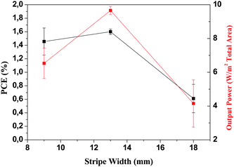 | ||
| Fig. 8 The power that can be extracted from a module aperture as a function of stripe width and the nominal power conversion efficiency obtained for the modules with 9, 13 and 18 mm wide stripes. All devices were prepared using the same silver ink (PV410). | ||
Ideally the stripe should be as narrow as possible to minimize the Ohmic loss and as wide as possible to maximize the active area. Since the serial connection of stripes takes up some of the active area (Fig. 1) the increased performance due to narrowing of the stripe is quickly lost due to the inactive area from the serial interconnections. In Fig. 1 the gaps between the ITO stripes are shown along with the positioning of the different layers to avoid short circuit and to achieve interconnection. Ideally the gap between the ITO stripes which is necessary to electrically isolate the individual stripes should be as small as possible. Also the gap between the slot-die coated stripes should be as small as possible. In practical terms it is very difficult to slot-die coat a narrower gap than 1 mm at low speeds (<60 m min−1) due to both the mask and the coating behaviour of liquids and the aperture loss from a gap larger than 3 mm are too excessive. During this work gaps of 1, 2 and 3 mm have been employed and 2 mm is the gap width that gives the largest degree of control. It is however highly feasible to employ 1 mm gap but it challenges the skill of the experimenter doing the coating. The optimum device geometry thus includes the physical properties of the materials (sheet resistivity, conductivity, optical transmission), the tolerances that can be handled (masks, printing resolution) and the skill of the experimenter (technical yield). From the experiments carried out during these trials a stripe width of 13 mm and a gap of 2 mm was the best compromise between active area, technical yield and device performance as shown in Fig. 8. Further work thus concentrated on 13 mm wide ITO stripes with a 2 mm gap between the stripes. The results have been detailed in the following.
3.3 Effect of module length
The rational choice of ITO stripe width (13 mm) and gap width (2 mm) was further investigated with a detailed cost and performance analysis in mind. The length of ITO stripes were either 200 mm or 225 mm. The reason for the two different lengths was to enable as many different module lengths as possible. In principle the length of the module should not influence the performance described above as the current flow (and voltage) is between the stripes and not along them.The role of defects and coating errors cannot be ruled out and thus the longer the stripe the larger the chance of defects. It was thus expected that all modules should exhibit roughly the same average performance but that the spread in performance would be larger for the smaller modules. An additional complication for the 60 and 100 mm modules are that they share the same ITO and PEDOT:PSS stripe and therefore the active area had to be carefully masked to avoid light harvesting from areas outside the nominal module aperture. The data has been summarized in Fig. 9 and Table 2 where it is evident that the larger modules have a lower average PCE but a large spread due to a large spread in the short circuit current. The smaller modules have a smaller spread.
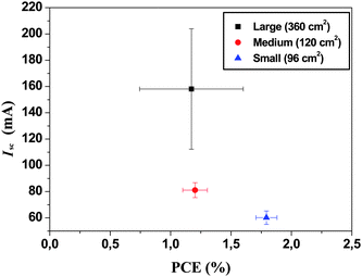 | ||
| Fig. 9 I sc versus PCE for the three different module lengths employed with 13 mm wide ITO stripes and a 2 mm gap. | ||
| Module Size | Max PCE (%) | Mean PCE (%) | Mean Isc/mA | Mean Voc/V | Mean FF (%) |
|---|---|---|---|---|---|
| Large (360 cm2) | 1.69 | 1.18 (±0.13) | 185.8 (±13.0) | 7.83 (±0.21) | 36.7 (±1.7) |
| Medium (160 cm2) | 1.36 | 1.22 (±0.11) | 81.0 (±5.8) | 6.81 (±0.17) | 34.8 (±1.0) |
| Small (96 cm2) | 2.00 | 1.79 (±0.09) | 60.1 (±5.1) | 7.56 (±0.12) | 37.9 (±2.1) |
3.4 Silver inks
The most enabling features of the inverted geometry are that it is the possible to print a metal electrode such as silver that can be used as the hole-collecting electrode. In addition to being beneficial in the context of device stability it also allows for processing under ambient conditions thus alleviating the need for glovebox conditions and vacuum steps. There are however some challenges associated with the use of printable silver inks as these contain solvents that may adversely affect the already printed layers. In this process the silver is applied in the final printing step meaning that the wet silver ink has to reside on top of the active layers until dried. The are several solutions to this and the most obvious is to chose a silver ink with a solvent that is not harmful to the underlying layers. While silver inks are commercially available with different solvent mixtures and polarity types it is not unproblematic. In the devices prepared here the active layer and the PEDOT:PSS layer are susceptible to solvents and while the solvents employed for their preparation were orthogonal it is difficult to find a silver ink with a solvent mixture that is orthogonal to both the active layer and the PEDOT:PSS layer. The initial experiments all failed to give devices with a significant open-circuit voltage (Voc) due to short circuits induced by the solvents in the silver ink. The devices could be tested before application of the silver ink by contacting the PEDOT:PSS showing that the open-circuit voltage was there while current extraction was poor due to the low conductivity of the PEDOT:PSS. Upon application of the silver electrode the devices failed initially. AFM studies on the surface of the active layer films (Fig. 10) before and after printing of silver showed significant differences in morphology and surface roughness.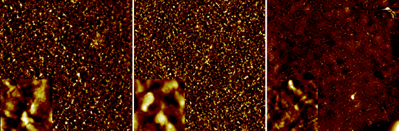 | ||
| Fig. 10 AFM images of the active layer surface post production and after delamination at the active layer–PEDOT:PSS interface. The images are 100 × 100 μm (insets are 5 × 5 μm). The surface of the active layer beneath printed silver was visibly different and with a roughness of 40 nm (left). The surface underneath PEDOT:PSS without the print was smoother with a roughness of 25 nm (middle). The devices that were pre-washed with isopropanol during coating of PEDOT:PSS were much smoother underneath the printed silver with a roughness of 20 nm (right). | ||
It was found that the devices that were pre-washed with isopropanol during coating of the PEDOT:PSS gave rise to a much smother film at the active layer-PEDOT:PSS interface after printing silver on top. We thus ascribe the roughness to be induced by the solvents in the silver ink and to be responsible for the short circuits. The isopropanol pre-washing was found to alter the surface morphology and to enable printing of the silver without inducing short circuits. In Fig. 11 and Table 1 we show results from printing using different commercially available screen printable silver inks. It should be emphasized that all the inks are highly performing and all give rise to the specified performance in terms of conductivity, drying, printability, ITO contacting etc. The variation in performance has to be viewed in the context of this process that specifically requires printing on top of a PET/ITO/ZnO/P3HT:PCBM/PEDOT:PSS composite film.
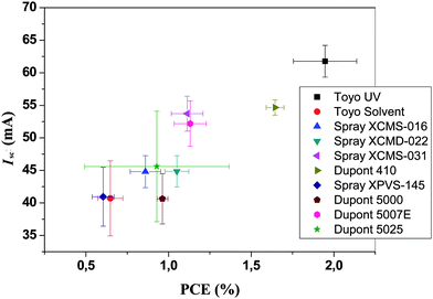 | ||
| Fig. 11 I sc versus PCE for ten different commercial silver inks tested on 96 cm2 area modules. | ||
The main reasons for employing the silver back electrode in the form of a silver grid was to allow for semi-transparency, reduction of cost, enabling faster drying and to minimize the influence of diffusion of solvents from the silver ink into the active layers. It should be emphasized that the use of a silver grid and consequent achievement of semi-transparency is possible due to the reasonable conductivity of the PEDOT:PSS layer and it would not be possible to employ a silver grid in case of hole-transporting oxides (i.e. V2O5, WO3, MoO3) back electrodes where a fully covering back electrode is required.
The silver inks that generally performed well were those with a high silver content (80–86% wt/wt) and those that did not perform so well generally had a lower silver content and consequently more solvent. Also the high-silver-content inks generally had a higher viscosity resulting in slower diffusion of solvents out of the ink. Generally the time from printing to drying was kept as short as possible (<1 min) to avoid excessive diffusion of solvents into the active layer. One of the tested inks employed UV curing and was as such solvent-free. This ink performed exceptionally well and we ascribe this advantage to the fact that the silver is mixed with a UV-cross linkable prepolymer. A secondary advantage of this ink was that it is not soluble in solvents after curing in contrast to all the other inks.
3.5 Performance, stability and reproducibility
After printing of the polymer, it was encapsulated by laminating a barrier foil from Alcan25 on both sides of the device. The printed side was laminated first. The encapsulation was carried out using the machine shown in Fig. 5. The multi-purpose laminator was used for firstly applying the adhesive to the barrier foil and secondly for application of the barrier material on both sides and thirdly for edge trimming of the foil.The front side of the solar cell was fully laminated with barrier foil and the backside (the printed side) was laminated with material having a width such that some of the printed silver electrodes were exposed. This enabled roll-to-roll characterisation of the solar cells as shown in Fig. 6. This proved to be an excellent tool in several aspects. When roll coating it is very easy to adjust or deliberately vary a coating parameter during coating and since each module on the roll has a specific label it is easy to probe the effect of the change or alteration when finally characterising the whole roll. Typical variables are coating speed, wet thickness, drying temperature etc. This proved to be a powerful tool in the optimisation scheme. An example has been outlined in Fig. 12 where the PCE for the modules has been plotted as a function of the number on the roll. It is the 60 mm modules spaced by 25 mm. A variation in the wet thickness of the active layer is clearly reflected as a step in performance. The roll-to-roll characterisation can thus be used as a quality control tool and in the context of research and development for process optimisation. The roll-to-roll characterisation of the solar cells could also be used for annealing the modules while characterising such that a consistent comparison between the modules could be made. The devices printed with UV-curable silver ink were very close to fully operational “as prepared” due to UV-activation of the ZnO during UV-curing whereas the all the modules prepared using thermally dried silver inks required light soaking for some time before the optimum performance was reached. To further explain this, some experiments were carried out to highlight the dependence of UV light and oxygen on the initial device performance. The encapsulation of the devices employs a multilayer barrier film with a UV filter having a cut-off at around 380 nm. Without the UV filter the devices work immediately but will operate for a significantly shorter time due to the UV-induced degradation. In the absence of UV the devices initially work poorly as illustrated in Fig. 13 where continuous IV scans are shown as a function of time. The devices however gradually improve over the course of 15–30 min.
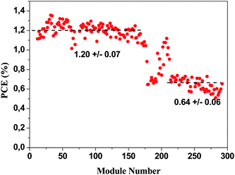 | ||
| Fig. 12 A plot of the module PCE along a roll of 60 mm modules. The plot shows the spread in performance that amounts to around ±10% around the average value. Upon changing the wet thickness of the active layer a step change in performance is observed. | ||
 | ||
| Fig. 13 Evolution of the IV curves of a freshly prepared device after encapsulation. The illumination was continuous (1000 W m−2, AM 1.5 G, 72 ± 2 °C). The device improves over the course of 15 min from 0.5% to 1.06% power conversion efficiency. | ||
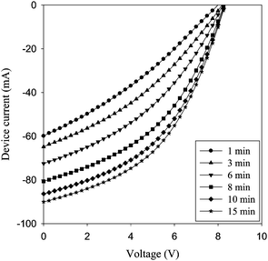
In order to explain the behaviour we performed experiments with and without UV light and found that the interaction with oxygen corroborates well with the reported photoconductivity of ZnO.47 We propose that the interactions shown in Fig. 14 are in place which is in agreement with earlier observation made on memory devices based on ZnO.47 The initially prepared ZnO device thus has oxygen adsorbed on the surface of the ZnO nanoparticles that act as traps for electrons leading to poor transport.
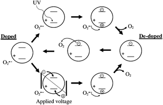 | ||
| Fig. 14 Proposed mechanism and interaction of ZnO nanoparticles with oxygen and UV light. The charges denoted as ± are bound charges whereas the encircled charges are mobile. The initially doped state can become de-doped by application of a voltage or by application of UV light. The oxygen present will gradually re-absorb on the surface and re-dope the ZnO nanoparticles. | ||
In the presence of UV light the direct bandgap excitation of the ZnO will lead to free carriers and immediate conductivity. The insertion of a UV filter at this point will lead to poor conductivity again. During longer UV irradiation the oxygen is gradually de-doped by some of the holes generated in the ZnO and the conductivity becomes permanent. The desorption of oxygen by direct excitation using UV light is thus a kinetically slow process. This observation was found to have significant impact on the speed at which the completed modules can be annealed and characterised (vide supra).
In terms of stability the devices perform quite well both during storage and operation which has enabled round robin studies between 18 different laboratories,25 sharing of cells between laboratories but also demonstration projects,19 prototyping and product simulation (vide supra). The operational stability of 16 stripe 225 mm devices and 8 stripe 250 mm modules are shown in Fig. 15 under continuous illumination at two different incident light intensities and temperatures. In all cases the performance initially drops but in the cases of lower light intensity and lower temperature the performance increase over 200 h followed by a relatively steady level for 300 h with a slow decline. In the case of the higher intensity and higher temperature there is a short period with a slight increase or a steady performance followed by an exponential decay over the remaining 450 h. In cases where a particular device exhibits degradation in performance it is normal to quote some measure of the lifetime or stability. OPVs are known to exhibit many different degradation curves. When plotting the performance as a function of time under continuous illumination the most typical examples of degradation behaviour include:
1) An initial increase or decrease in performance followed by a decay that may be linear or exponential
2) Linear or exponential decay from the very beginning
3) A fast initial decay followed by stabilisation and a much slower decay
4) Complex initial behaviour followed by any of the above
5) Any of the above with a sudden catastrophic failure
The time from the start of the measurement to the point at which the device yields 80% of the initial performance (often termed T80) or the time to the point at which the device yields half the initial performance (often termed half life or T50) are measurable parameters that in principle can be used to compare device stability and operational lifetime. It is however debatable where the starting point should be taken and the most rational choice is possibly that T80 (or T50) is quoted as the time from the maximum achievable performance. It is obvious that unless the actual degradation is shown from the very start of device life (i.e. from when freshly prepared) it gives little meaning to compare different device geometries. As an example a cell that drops linearly to half its value in 100 h and then remains within 20% of that value for 10![[hair space]](https://www.rsc.org/images/entities/char_200a.gif) 000 h would have a T80 of 40 h if measuring form the beginning. If however the supplier quotes the performance as about half the initial performance then the T80 would be 10000 h. In the end the people applying the solar cell will decide what the real T80 is. When looking at Fig. 13 at the devices tested at 280 W m−2 and 45 ± 5 °C it is clear that the devices drop in performance during the first 5 h of operation by a factor of three. The T80 would in this case be around 1 h. The device then increases steadily for 200 h and then starts to degrade slowly. It is clear that the device exhibits quite stable performance from this point onwards and would present a T80 of around 300 h. The question is whether one could expect the user to wait the 200 h it takes to reach the specified performance. The best solution to this answer is quite possibly to solve the technical problems before attempting practical use of the modules presented in Fig. 15. In any case the use of OPV can be expected to require new ways of thinking about application and specification of performance.
000 h would have a T80 of 40 h if measuring form the beginning. If however the supplier quotes the performance as about half the initial performance then the T80 would be 10000 h. In the end the people applying the solar cell will decide what the real T80 is. When looking at Fig. 13 at the devices tested at 280 W m−2 and 45 ± 5 °C it is clear that the devices drop in performance during the first 5 h of operation by a factor of three. The T80 would in this case be around 1 h. The device then increases steadily for 200 h and then starts to degrade slowly. It is clear that the device exhibits quite stable performance from this point onwards and would present a T80 of around 300 h. The question is whether one could expect the user to wait the 200 h it takes to reach the specified performance. The best solution to this answer is quite possibly to solve the technical problems before attempting practical use of the modules presented in Fig. 15. In any case the use of OPV can be expected to require new ways of thinking about application and specification of performance.
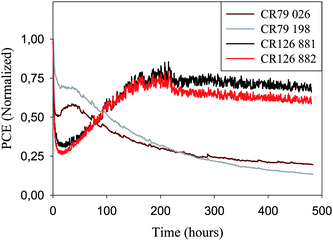 | ||
| Fig. 15 Operational stability of two 16 stripe 225 mm modules (280 W m−2, AM 1.5 G, 45 ± 5 °C) and two 8 stripe 250 mm modules (1000 W m−2, AM 1.5 G, 85 ± 5 °C) tested for 480 h. The two modules that were adjacent on the roll (CR 126 881/882, 280 W m−2, AM1.5G) exhibit quite similar performance and operational lifetime behavior while two modules that were at opposite ends of the roll (CR 79 26/198, 1000 W m−2, AM1.5G) exhibit some variation in operational lifetime and performance. | ||
3.6 Upscaling and manufacture
Data from the testing trials made it is clear that the technology is highly scalable and that manufacture and upscaling is highly feasible. The scale tested so far has mostly involved a web width of 305 mm and devices with sizes that are approximately the size of an A4 sheet while experiments have been made with a web width of 610 mm (also shown in Fig. 16).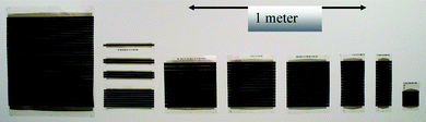 | ||
| Fig. 16 Examples of the scale on which modules have been prepared. Modules from about 50 × 50 cm2 (left) to 10 × 10 cm2 (right) are shown. The devices span from single stripe cells to serially connected modules where the smallest module has 2 serially connected stripes and the largest has 38 serially connected stripes. Stripe widths from 5 to 18 mm are shown. | ||
In Fig. 16 several of the module sizes tested are shown and they range from 50 × 50 cm2 to 10 × 10 cm2 and comprise from single stripes through 2 to 38 serially connected stripes in stripe widths from 5 to 18 mm. Experience have shown that there are no technical differences between the various modules except one of increased cost during experimentation for the larger modules. The typical webs speeds that have been involved are 1–2 m min−1 and in total Risø DTU have prepared more than 1000 square metres of OPV in 2009 alone on the small equipment described in the following.
3.7 Cost analysis and investment in manufacturing equipment
The cost estimates for polymer solar cells have been reported as very low with a potential electricity cost well below 0.5 € Wp−1. Most of the arguments in the literature that are in favour of this view suffer from the fact that no real data are given and critics may argue that the cost estimates are based on fiction rather than fact. In addition, the cost of electricity from OPV should be quoted as the levelized cost of electricity (LCOE) as this takes the operational lifetime of the device into account. There have been a few reports on the manufacture of polymer solar cells where a rigid cost analysis was detailed including the actual cost of materials and manufacturing labour thus enabling a better view of the capacity of the OPV technology in terms of cost. One example detailed the manufacture of a small solar cell prepared entirely by screen printing of all the layers using existing industrial equipment where the capital investment in equipment is zero.19A second example detailed the manufacture and integration of discrete electronic components in a single application for the lighting Africa initiative.48,49 The purpose of the first demonstration was to charge a battery for powering a radio at a music festival and the second demonstration was intended to provide inhabitants in developing countries with light without the need for kerosene lamps. Both demonstrations were carried out in public and the cost structure have enabled the analysis of how well the technology performs in the context of electricity production50,51 and more notably allowed for the identification of where investments in efforts to reduce the cost are best placed.48,50,51 In the case of the solar hat19 that was prepared entirely using screen printing with the consequent limitations on performance gave an electricity cost of 4500 € Wp−1. In the case of the lamp for the lighting Africa initiative a practical electricity cost of 35 € Wp−1 was achieved. When looking at the solar cells prepared in this study where the cost was further reduced through optimisation of the usage of ink and by purchasing larger quantities of materials at lower cost a learning curve can be plotted as shown in Fig. 17.
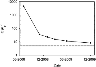 | ||
| Fig. 17 Learning curve for the manufacturing cost in € Wp−1 for R2R manufacture polymer solar cells based on ProcessOne (ref. 21). The lowest achievable cost with P3HT:PCBM and ITO using ProcessOne is estimated to be around 5 € Wp−1 shown as a broken line. Note that the first point is based on the solar hat (ref. 19) which differs slightly from ProcessOne with respect to materials and printing technology. | ||
The lowest electricity cost that can be achieved when manufacturing modules based on ProcessOne using P3HT:PCBM on ITO is estimated to be ca. 5 € Wp−1. The lowest cost reached to date with the equipment described, the current usage of materials and the materials cost on the scale of these experiments is 8.1 € Wp−1. It should be noted that the investment in man power and processing time already contribute very little (<20%) to the total cost which is essentially limited to the cost of materials. Further reductions have to come from: elimination of the expensive components such as ITO, an increase of the processing speed (e.g. by more than a factor of 10) and possibly from lower costs for PEDOT:PSS and the active materials through significant upscaling on the part of chemical suppliers, and possibly through elimination of one adhesive layer (Table 3). It is clear that new high-performing active materials could enter Table 3 and give significantly lower cost in € Wp−1 provided that they have a similar cost to the P3HT:PCBM composite. It should also be noted that the manufacturing cost shown in Table 3 excludes the cost associated with characterisation of the final module. The cost of characterisation using the equipment described in section 2.6 is quite low and around 0.005 € per IV curve based on the power consumption of the R2R characteriser. The costs per kWh of electricity and the typical positioning time including recording of the IV curve are respectively 2.2 kW, 0.265 € and 30 s. The annealing time required for ProcessOne however requires long testing times if a particular performance is to be guaranteed. With a typical annealing time of 20 min the extra cost of characterization is 0.194 € module−1. While this is not prohibitive in terms of cost it limits the production capacity to the production speed to the annealing time. The typical total manufacturing time is in the range of 42–95 s per module. This manufacturing time is the total manufacturing time starting from a PET substrate fully covered with ITO. It is clear that the annealing time exceeds the manufacturing time by a factor of approximately 20. With the currently accessible lifetimes for OPV however the LCOE is not even close to being competitive as detailed above whereas the cost of electricity for freshly prepared cells is likely to be competitive with inorganic solar cells on a small scale. This shows that low cost manufacture of OPV with a competitive performance is possible while work on improving the operational stability must be carried out to decrease the LCOE. When looking at the capital investment in manufacturing equipment this is generally viewed as low for the OPV technology and range as low as zero in cases where existing equipment can be used. This was the case for the solar hat19 that demonstrated manufacture using existing industrial equipment and infrastructure albeit with low performance. It is of some interest to show what the capital investment in equipment is to enable manufacture on the scale described here. All the equipment described above has been summarized in Table 4. The cost for the machinery and the investment in infrastructure (in a Danish setting) are shown. The machine park quoted is enough to enable full R2R manufacture and characterisation of the polymer solar cell modules described here. The realistic production capacity with the speeds achieved here is optimistically about 100 metres per day (assuming one 8 h shift). This gives an annual production capacity of around 20000 metres equivalent to 80000 modules described in Table 3 or 50 kWp assuming a technical yield of 95%. With the ∼530 k€ investment in equipment shown in Table 4 it is unlikely that this is financially viable at an electricity cost of 8 € Wp−1 and it is almost certain that one would be required to offer the OPVs at a significantly higher cost to enable a viable business structure. This still requires that customers are available in the competitive and relatively small thin film PV market. The above assumes that the R2R characterisation is not required as this would reduce the annual throughput to about 26000 of the modules described in Table 3 assuming that the R2R characteriser spends 20 min on each module and runs 24 h a day which is realistic.
| Material | Material cost/€ | Processing cost/€ | Total/€ |
|---|---|---|---|
| Barrier | 0.4575 | 0.03173 | 0.4892 |
| Pressure sensitive adhesive | 0.1918 | 0.03173 | 0.2236 |
| PET-ITO | 2.6077 | 0.21111 | 2.8188 |
| ZnO | 0.0582 | 0.16667 | 0.2249 |
| P3HT-PCBM | 0.4492 | 0.16667 | 0.6159 |
| PEDOT:PSS (EL-P 5010) | 0.2311 | 0.16667 | 0.3978 |
| Silver (PV410) | 0.4120 | 0.16667 | 0.5787 |
| Total | 4.4078 | 0.9412 | 5.3491 |
| Equipment | Machine cost/€ | Infrastructure/€ | Total/€ |
|---|---|---|---|
| a Includes both hot air dryer and UV-curing oven. b Includes edge guiding system, humidity sensors and corona treater. c Includes solar simulator (KHS1200), source meter (Keithley 2400), power meter, control electronics and pneumatic control. | |||
| R2R Screen printer (Alraun)a | 126400 |
35800 |
162200 |
| R2R Slot-die Coater (SCM)b | 152000 |
18500 |
170500 |
| R2R Etching machine (Asia) | 42500 |
9500 |
52000 |
| R2R Laminator (GM) | 35800 |
0 | 35800 |
| R2R Characteriser (Risø DTU)c | 72850 |
0 | 72850 |
| R2R Sheeter (GM) | 28900 |
0 | 28.900 |
| Contactor (Prym) | 8000 |
0 | 8000 |
| Total |
466![[hair space]](https://www.rsc.org/images/entities/b_char_200a.gif) 450 450
|
63800
|
530250
|
It is possible to heat treat the solar cells by passage of the roll through an oven at temperatures of 120–140 °C and thus reduce the required annealing time to 1–2 min. It is however associated with some problems of deformation of the foil since the barrier material is not heat stabilized and when heating a multilayer foil where some layers deform upon heating the shape of the final modules is not predictable.
3.8 Examples of application
As with any new technology its demonstration precedes its useful application. There have been several public demonstrations of the OPV technology as shown in Fig. 18 starting in 2008 at the Roskilde music festival where a screen printed solar cell module was used to charge a battery for a small FM radio. In 2009 there have been several more examples including the grid connection of OPV, its use in a mobile curtain in conjunction with phase change materials demonstrating a semi-transparent sun blind comprising 91 modules that provided electricity for illumination and charging purposes.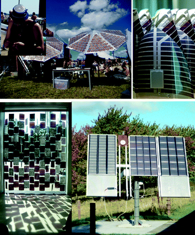 | ||
| Fig. 18 Photographs of various OPV demonstration projects. The solar hat (ref. 19) is shown (top left), the lamp for the Lighting Africa initiative (top right), the mobile curtain Suntiles™ that was designed by Astrid Krogh and displayed publically at the Danish Design Centre during autumn/winter 2009/2010 (bottom left) and the grid connected OPV modules (panel size: 1 m × 1.7 m) mounted on a solar tracking station (bottom right). | ||
Finally the complete manufacture of a low cost flexible and very light weight LED based lamp that can be recharged by sunlight for the Lighting Africa initiative.48,49 The practical results from the demonstration projects have convincingly shown that OPVs can be manufactured for specific purposes on a reasonable scale and they work well. These experiences have also revealed that there is still a large room for improvement in terms of developing design tools such that the application is well matched to the capacity of the solar cell in addition to improving the materials and constitution of the technology. Significant problems are the mechanical stability which is a relatively unexplored area that present significant problems such as delamination at interfaces and mechanically stable electrical contacts.
3.9 Future room for improvement and outlook
There are a few areas that will need to see significant development before we can expect OPV to become an industrially significant photovoltaic technology and these are in turn significant reductions in materials usage and alleviation of ITO and possibly PEDOT:PSS. By increasing the manufacturing speed further and possibly by having inline coating systems where all layers are coated in the same pass through the machine the manufacturing cost can possibly be reduced to below 5% of the total module cost. In order to become competitive with existing technologies in terms of LCOE the operational stability also needs to be improved significantly. A significantly improved power conversion efficiency would greatly aid the applicability of the technology and it is likely that the active area power conversion efficiency has to reach 10% before a stable cost structure can be realized.4. Conclusion
We have described efforts towards upscaling the manufacture of polymer solar cells using full roll-to-roll processing and show that it is possible to prepare and scale large polymer solar cells on a size below 1 metre. We conclude that further upscaling to web widths of 1–2 meters should be possible. In terms of manufacturing speed we have explored web speeds in the range of 0.2–2 m min−1 and we expect that this can be increased 10-fold without further development but that processing speeds above 20 m min−1 will be required to realize the low cost potential of the OPV technology. These developments will come after further investment in research. We further conclude that the capital investment in manufacturing equipment is low while the Wp production capacity is too low to be financially viable and significant improvements in processing speed and reduction of materials cost will be required to enable a stable cost structure. In addition, the use of oxide semiconducting materials includes problems of dynamic IV curve behaviour that requires long annealing times. If this is not efficiently solved for ProcessOne it is likely to be prohibitive for successful commercialization of that particular OPV technology. We further show that demonstration projects are a very useful tool to test OPV as a new technology and provide feedback for further development into a viable and available PV solution.Acknowledgements
This work was supported by the Danish Strategic Research Council (DSF 2104-05-0052 and 2104-07-0022), by EUDP (j. nr. 64009-0050) and by PV-ERA-NET (project acronym POLYSTAR). Torben Kjær and Jan Alstrup are gratefully acknowledged for technical assistance. We further thank Jan Fyenbo at Mekoprint Electronics A/S for preparing the patterned ITO. We thank Astrid Krogh for designing the sun blind. We thank Lasse Gorm Jensen from Nyhedshuset Ingenøren A/S for creating the illustrative graphics of the flexible solar cell.References
- S. Günes, H. Neugebauer and N. S. Sariciftci, Chem. Rev., 2007, 107, 1324–1338 CrossRef.
- E. Bundgaard and F. C. Krebs, Sol. Energy Mater. Sol. Cells, 2007, 91, 954–985 CrossRef CAS.
- B. C. Thompson and J. M. J. Fréchet, Angew. Chem., Int. Ed., 2008, 47, 58–77 CrossRef.
- M. Jørgensen, K. Norrman and F. C. Krebs, Sol. Energy Mater. Sol. Cells, 2008, 92, 686–714 CrossRef.
- F. C. Krebs, Sol. Energy Mater. Sol. Cells, 2009, 93, 394–412 CrossRef CAS.
- T. Ameri, G. Dennler, C. Lungenschmied and C. J. Brabec, Energy Environ. Sci., 2009, 2, 347–363 RSC.
- G. Dennler, M. C. Scharber and C. J. Brabec, Adv. Mater., 2009, 21, 1323–1338 CrossRef CAS.
- M. Helgesen, R. Søndergaard and F. C. Krebs, J. Mater. Chem., 2010, 20, 36–60 RSC.
- J. Y. Kim, K. Lee, N. E. Coates, D. Moses, T.-Q. Nguyen, M. Dante and A. J. Heeger, Science, 2007, 317, 222–225 CrossRef CAS.
- S. H. Park, A. Roy, S. Beaupré, S. Cho, N. Coates, J. S. Moon, D. Moses, M. Leclerc, K. Lee and A. J. Heeger, Nat. Photonics, 2009, 3, 297–303 Search PubMed.
- H.-Y. Chen, J. Hou, S. Zhang, Y. Liang, G. Yang, Y. Yang, L. Yu, Y. Wu and G. Li, Nat. Photonics, 2009, 3, 649–653 Search PubMed.
- E. A. Katz, S. Gevorgyan, M. S. Orynbayev and F. C. Krebs, Eur. Phys. J.: Appl. Phys., 2006, 36, 307–311 CrossRef CAS.
- F. C. Krebs and K. Norrman, Progr. Photovolt.: Res. Appl., 2007, 15, 697–712 Search PubMed.
- J. A. Hauch, P. Schilinsky, S. A. Choulis, R. Childers, M. Biele and C. J. Brabec, Sol. Energy Mater. Sol. Cells, 2008, 92, 727–731 CrossRef CAS.
- F. C. Krebs, Sol. Energy Mater. Sol. Cells, 2008, 92, 715–726 CrossRef CAS.
- F. C. Krebs, Y. Thomann, R. Thomann and J. W. Andreasen, Nanotechnology, 2008, 19, 424013 CrossRef.
- B. Zimmermann, U. Würfel and M. Niggemann, Sol. Energy Mater. Sol. Cells, 2009, 93, 491–496 CrossRef.
- K. Norrman, S. A. Gevorgyan and F. C. Krebs, ACS Appl. Mater. Interfaces, 2009, 1, 102–112 Search PubMed.
- F. C. Krebs, M. Jørgensen, K. Norrman, O. Hagemann, J. Alstrup, T. D. Nielsen, J. Fyenbo, K. Larsen and J. Kristensen, Sol. Energy Mater. Sol. Cells, 2009, 93, 422–441 CrossRef CAS.
- F. C. Krebs, Sol. Energy Mater. Sol. Cells, 2009, 93, 465–475 CrossRef CAS.
- F. C. Krebs, S. A. Gevorgyan and J. Alstrup, J. Mater. Chem., 2009, 19, 5442–5451 RSC.
- F. C. Krebs, Sol. Energy Mater. Sol. Cells, 2009, 93, 1636–1641 CrossRef CAS.
- F. C. Krebs, Org. Electron., 2009, 10, 761–768 CrossRef CAS.
- B. Zimmermann, M. Glatthaar, M. Niggemann, M. K. Riede, A. Hinsch and A. Gombert, Sol. Energy Mater. Sol. Cells, 2007, 91, 374–378 CrossRef CAS.
- F. C. Krebs, S. A. Gevorgyan, B. Gholamkhass, S. Holdcroft, C. Schlenker, M. E. Thompson, B. C. Thompson, D. Olson, D. S. Ginley, S. E. Shaheen, H. N. Alshareef, J. W. Murphy, W. J. Youngblood, N. C. Heston, J. Reynolds, S. Jia, D. Laird, S. M. Tuladhar, J. G. A. Dane, P. Atienzar, J. Nelson, J. M. Kroon, M. M. Wienk, R. A. J. Janssen, K. Tvingstedt, F. Zhang, M. Andersson, O. Inganäs, M. Lira-Cantu, R. de Bettignies, S. Guillerez, T. Aernouts, D. Cheyns, L. Lutsen, B. Zimmermann, U. Würfel, M. Niggemann, H.-F. Schleiermacher, P. Liska, M. Grätzel, P. Lianos, E. A. Katz, W. Lohwasser and B. Jannon, Sol. Energy Mater. Sol. Cells, 2009, 93, 1968–1977 CrossRef CAS.
- F. C. Krebs and M. Jørgensen, WO Pat., 2007118850 A1.
- M. Jørgensen, O. Hagemann, J. Alstrup and F. C. Krebs, Sol. Energy Mater. Sol. Cells, 2009, 93, 413–421 CrossRef CAS.
- T. Aernouts, P. Vanlaeke, W. Geens, J. Poortmans, P. Heremans, S. Borghs, R. Mertens, R. Andriessen and L. Leenders, Thin Solid Films, 2004, 451–452, 22–25 CrossRef.
- B. Winther-Jensen and F. C. Krebs, Sol. Energy Mater. Sol. Cells, 2006, 90, 123–132 CrossRef CAS.
- J.-Y. Lee, S. T. Connor, Y. Cui and P. Peumans, Nano Lett., 2008, 8, 689–692 CrossRef CAS.
- M. Strange, D. Plackett, M. Kaasgaard and F. C. Krebs, Sol. Energy Mater. Sol. Cells, 2008, 92, 805–813 CrossRef CAS.
- K. Tvingstedt and O. Inganäs, Adv. Mater., 2007, 19, 2893–2897 CrossRef CAS.
- O. Hagemann, M. Bjerring, N. C. Nielsen and F. C. Krebs, Sol. Energy Mater. Sol. Cells, 2008, 92, 1327–1335 CrossRef CAS.
- http://www.plextronics.com/ .
- L. M. Campos, A. J. Mozer, S. Günes, C. Winder, H. Neugebauer, N. S. Sariciftci, B. C. Thompson, B. D. Reeves, C. R. G. Grenier and J. R. Reynolds, Sol. Energy Mater. Sol. Cells, 2006, 90, 3531–3546 CrossRef CAS.
- M. Lira-Cantu and F. C. Krebs, Sol. Energy Mater. Sol. Cells, 2006, 90, 2076–2086 CrossRef CAS.
- D. C. Olson, J. Piris, R. T. Collins, S. E. Shaheen and D. S. Ginley, Thin Solid Films, 2006, 496, 26–29 CrossRef CAS.
- W. J. E. Beek, M. M. Wienk, M. Kemerink, X. Yang and R. A. J. Janssen, J. Phys. Chem. B, 2005, 109, 9505–9516 CrossRef CAS.
- D. C. Olson, Y.-J. Lee, M. S. White, N. Kopidakis, S. E. Shaheen, D. S. Ginley, J. A. Voigt and J. W. P. Hsu, J. Phys. Chem. C, 2007, 111, 16640–16645 CrossRef CAS.
- D. C. Olson, S. E. Shaheen, R. T. Collins and D. S. Ginley, J. Phys. Chem. C, 2007, 111, 16670–16678 CrossRef CAS.
- D. C. Olson, S. E. Shaheen, M. S. White, W. J. Mitchell, M. F. A. M. van Hest, R. T. Collins and D. S. Ginley, Adv. Funct. Mater., 2007, 17, 264–269 CrossRef CAS.
- C. Waldauf, M. Morana, P. Denk, P. Schilinsky, K. Coakley, S. A. Choulis and C. J. Brabec, Appl. Phys. Lett., 2006, 89, 233517 CrossRef.
- M. Lira-Cantu, K. Norrman, J. W. Andreasen and F. C. Krebs, Chem. Mater., 2006, 18, 5684–5690 CrossRef CAS.
- J. S. Huang, C. Y. Chou, M. Y. Liu, K. H. Tsai, W. H. Lin and C. F. Lin, Org. Electron., 2009, 10, 1060–1065 CrossRef CAS.
- C. Tao, S. Ruan, G. Xie, X. Kong, L. Shen, F. Meng, C. Liu, X. Zhang, W. Dong and W. Chen, Appl. Phys. Lett., 2009, 94, 043311 CrossRef.
- T. Hori, T. Shibata, V. Kittichungchit, H. Moritou, J. Sakai, H. Kubo, A. Fujii and M. Ozaki, Thin Solid Films, 2009, 518, 522–525 CrossRef CAS.
- F. Verbakel, S. C. J. Meskers and R. A. J. Janssen, Appl. Phys. Lett., 2006, 89, 102103 CrossRef.
- F. C. Krebs, T. D. Nielsen, J. Fyenbo, M. Wadstrøm and M. S. Petersen, Energy Environ. Sci., 2010, 3, 512–525 Search PubMed.
- http://www.lightingafrica.org/ .
- C. Powell, T. Bender and Y. Lawryshyn, Sol. Energy, 2009, 83, 1977–1984 CrossRef CAS.
- J. Kalowekamo and E. Baker, Sol. Energy, 2009, 83, 1224–1231 CrossRef CAS.
| This journal is © The Royal Society of Chemistry 2010 |