Properties, synthesis, and growth mechanisms of carbon nanotubes with special focus on thermal chemical vapor deposition
Gilbert D.
Nessim
*ab
aDepartment of Materials Science and Engineering, Massachusetts Institute of Technology, 77 Massachusetts Avenue, Cambridge, MA 02139, USA. E-mail: gdnessim@mit.edu
bDepartment of Chemistry, Bar Ilan University, Ramat Gan, 52900, Israel
First published on 28th May 2010
Abstract
Carbon nanotubes (CNTs) have been extensively investigated in the last decade because their superior properties could benefit many applications. However, CNTs have not yet made a major leap into industry, especially for electronic devices, because of fabrication challenges. This review provides an overview of state-of-the-art of CNT synthesis techniques and illustrates their major technical difficulties. It also charts possible in situ analyses and new reactor designs that might enable commercialization. After a brief description of the CNT properties and of the various techniques used to synthesize substrate-free CNTs, the bulk of this review analyzes chemical vapor deposition (CVD). This technique receives special attention since it allows CNTs to be grown in predefined locations, provides a certain degree of control of the types of CNTs grown, and may have the highest chance to succeed commercially. Understanding the primary growth mechanisms at play during CVD is critical for controlling the properties of the CNTs grown and remains the major hurdle to overcome. Various factors that influence CNT growth receive a special focus: choice of catalyst and substrate materials, source gases, and process parameters. This review illustrates important considerations for in situ characterization and new reactor designs that may enable researchers to better understand the physical growth mechanisms and to optimize the synthesis of CNTs, thus contributing to make carbon nanotubes a manufacturing reality.
 Gilbert Daniel Nessim | Dr Gilbert Daniel Nessim received his Master's degree in Electrical Engineering from the École Centrale Paris in 1991 and from the Politecnico di Milano in 1993 within the framework of the Erasmus—TIME (Top Industrial Managers for Europe) program. He also received a DEA (Diplôme d’Études Approfondies) in optoelectronics from the Université Pierre et Marie Curie (Paris VI) in 1991 and a Master's in Business Administration (MBA) from INSEAD (France) in 1994. After graduation, he opted for an industrial career and worked in Research and Development at Otis Elevators, where he developed and patented an innovative infrared system for door detection. He also worked in management consulting firms, helping many high-tech companies to improve their R&D capabilities, and in entrepreneurial ventures. In 2004 he enrolled in the PhD program in the Materials Science and Engineering Department at MIT. His research, performed in the laboratory of Professor Carl V. Thompson, focused on the synthesis of carbon nanotubes for electrical applications. He received a two-year Fellowship from Intel Corporation and graduated in 2009. Dr Nessim is currently pursuing collaborative post-doctoral research between MIT and Bar Ilan University (Israel) focused on the synthesis of carbon nanostructures for more efficient batteries and supercapacitors. |
1. Background on carbon nanotubes
Carbon nanotubes (CNTs) research has exploded in the last decade with the hope to commercially exploit their truly remarkable properties.1–4 CNTs are the only material that combine all the following properties:5–8• 100 times stronger than steel9–11
• metallic or semiconducting behavior2
• in the case of metallic conduction, 100 times more conductive than copper over distances in the order of a micron12,13
• in the case of semiconducting behavior, the band gap depends on the nanotube diameter
• thermal conductivity matching that of diamond14,15
• very high melting temperature
• chemically inert but can be functionalized to modify specific properties (e.g., electrical conductivity16)
• structure close to an ideal one-dimensional (1-D) system with anisotropic properties,17 with diameters starting below 1 nm and aspect ratios that can exceed 1![[thin space (1/6-em)]](https://www.rsc.org/images/entities/char_2009.gif) 00000018–20
00000018–20
1.1 Historical overview
Although carbon nanotubes have been observed in a Damascus Sabre dated around the 17th century,21 the credit for the discovery of carbon nanotubes is not obvious. In a 2006 editorial to Carbon,22 Monthioux and Kuznetsov quote the 1889 patent that Hughes and Chambers23 filed to describe the method of producing carbon filaments for use as glow discharge elements in lamps using methane and ethylene as carbon sources. They proposed to use such filaments in the light bulbs that had just been presented by Edison at the Paris Universal Exposition that same year. Since the 1950's, there have been multiple reports of observations of carbon filaments that could have been CNTs, but the technology of the time did not allow to clearly characterize them.22,24,25The “official” birth date of carbon nanotubes is attributed to Dr Sumio Iijima from NEC who, in 1991, published a paper in Nature26 in which he reported the discovery of a “new type of finite carbon structure consisting of needle-like tubes” which comprises “coaxial tubes of graphitic sheets, ranging in number from 2 up to about 50”. This paper has been cited over 9000 times to date as almost every paper regarding nanotubes cites it (including this one!).
Since then, progress on carbon nanotubes has evolved at a very high pace,27 starting with the discovery of single-wall carbon nanotubes and methods to produce them using transition-metal catalysts27 by Bethune et al.28 at IBM and Iijima and Ichihashi29 at NEC, to electrical,30–33 mechanical,34 and medical35 applications.
1.2 Types of carbon nanotubes
Carbon structures can exhibit multiple allotropic forms, with very disparate properties from the soft and conductive graphite to the hard and insulating diamond. Fullerenes, also called buckyballs named after Richard Buckminster Fuller, are molecules composed entirely of carbon arranged in hexagonal and pentagonal rings (resembling the classic soccer balls), and can assume the form of a hollow sphere. Carbon nanotubes (CNTs) are another allotrope of carbon and, when synthesized, are often capped by a half fulllerene.There are two main structures of CNTs: single-wall CNTs (SWCNTs) and multi-wall CNTs (MWCNTs).36 An ideal single-wall carbon nanotube can be visualized as a rolled-up sheet of graphene (a sheet of carbon atoms arranged in hexagonal rings). The way the graphene sheet is wrapped is represented by a pair of indices (n,m) called the chiral vector, where the integers n and m represent the number of unit vectors along two directions in the honeycomb crystal lattice of graphene (Fig. 1). If m = 0, the nanotubes are called “zigzag”. If n = m, the nanotubes are called “armchair”. Otherwise, they are called “chiral”. An ideal multi-wall carbon nanotube can similarly be visualized as concentrically rolled-up sheets of graphene. It is important to notice that, although this is a good way to describe the structure and the atomic arrangement of nanotubes, it is inconsistent with the growth mechanisms that lead to their formation.
 | ||
| Fig. 1 Graphical representations of ideal graphene sheet, SWCNT, and MWCNT.36 Figure reprinted with permission from A. P. Graham, G. S. Duesberg, W. Hoenlein, F. Kreupl, M. Liebau, R. Martin, B. Rajasekharan, W. Pamler, R. Seidel, W. Steinhoegl and E. Unger, Appl. Phys. A: Mater. Sci. Process., 2005, 80, 1141–1151. Copyright 2005, Springer Berlin/Heidelberg. | ||
SWCNTs have a small diameter (from 0.4 nm to 4 nm) and exhibit the particular property that they can be metallic (semi-metals) or semiconducting, depending on their chirality.1,37 On average, meaning without chirality control, we obtain one third metallic (when n − m is a multiple of 3) and two thirds semiconducting SWCNTs (when n − m is not a multiple of 3). A single-wall CNT is considered perfectly crystalline (i.e. defect-free) if the graphene sheet has no variations in the hexagonal aromatic structure of the carbon atoms along the tube.
MWCNTs, which can be visualized as concentric SWCNTs, have a number of walls ranging from 2 (double-wall CNT) to less than a hundred. The diameter of a MWCNT can range from 1 nm and will rarely exceed 100 nm (beyond 100 nm, we can generally expect that the filament structure is a carbon fiber). In a MWCNT, the intertube distance is 0.34 nm, which is also the distance between two parallel graphene sheets in graphite. Given the ratio of metallic/semiconducting of 1/3 to 2/3 for SWCNTs, we can expect MWCNTs to be metallic, given that at least one of the walls will be metallic. Some teams have been able to grow monochiral MWCNTs, meaning that all walls have the same chirality.38
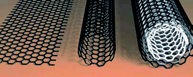
Ideally, crystalline SWCNTs and MWCNTs have walls and caps without any defects, missing or added atoms. This is extremely hard to attain with our current synthesis techniques and it is also difficult to properly characterize. Although teams have grown individual or strands of nanotubes with a length of a few centimetres,39 carpets of vertically aligned CNTs (VACNTs) do not exceed two centimetres40 at the time of this report.
A common type of defect is “bamboo” MWCNT, where the different walls cap at different lengths and appear as stacked. Carbon nanofibers, which consist of graphite platelets perfectly arranged in various orientations, are another type of filament formation that can be confused with MWCNTs. After reviewing many nanotube papers, it seems that a considerable fraction of them, especially the early CNT synthesis papers, report on nanotube growth although the investigated filaments were most likely fibers. The only way to be certain about the crystallinity of MWCNTs is to take high-resolution transmission electron microscopy (HRTEM) pictures, which is challenging and laborious.
1.3 Carbon nanotube properties
Because of their exceptional and anisotropic properties,1–4,41,42 carbon nanotubes (CNTs) have been widely investigated for electrical,43,44 thermal,45,46 and mechanical43,44,47 applications, such as microelectronic interconnects,48 heat sinks,46 and structural composites.49 This section will provide an overview of the most notable properties of carbon nanotubes, with a special emphasis on electrical properties.As a one dimensional object, the conductivity of a SWCNT contacted at both ends can be calculated using the Landauer equation:12,13,53

For a metallic SWCNT electrically contacted at both ends, in the absence of scattering, all Ti terms are equal to 1 and the resistance of a SWCNT is then R = 2RQ ≈ 13kΩ as a SWCNT has two conduction channels. The quantum resistance RQ = 6.5kΩ is due to the mismatch between the number of conduction channels in the nanotube and the macroscopic metallic contacts. Theoretical studies54,55 have indicated that ideal nanotubes are ballistic conductors for distances in the order of a micron. The one-dimensional confinement of electrons combined with the requirements for energy and momentum conservation leads to ballistic conduction.
To this ideal resistance, we need to add the scattering resistance due to impurities or nanotube defects, which reduces the mean free path compared to an ideal SWCNT (typically l0 = 1 µm):

If the nanotube length (l) is below one micron, we can usually neglect the scattering resistance. Once we contact the nanotube to a substrate or to a metallic contact, we need to consider an additional contact resistance, which strongly depends on the material in contact with the nanotube, and more specifically on the difference between the work functions of the SWCNT and of the electrode material. Shiraishi and Ata56 found the work functions of multi- and single-walled carbon nanotubes to be 4.95 eV and 5.10 eV respectively. Mann et al.57 demonstrated that highly reproducible ohmic contacts were obtained by contacting Pd leads to metallic SWCNTs. They also indicated that Pd contacts were more reliable than Ti contacts and that non-ohmic behavior was observed when CNTs were connected to Pt contacts.
We can model the resistance of a SWCNT contacted at each end as the sum of the three resistances discussed (note that the formula below applies also to MWCNTs):
| RCNT = RQ + RL + RCONTACT |
Assuming that we can neglect coupling between adjacent CNTs, which is usually a valid assumption as the electrons would rather travel through the ballistic path than through a large tunneling resistance (2–140 MΩ),58 the resistance of a bundle of SWCNTs can be viewed as a parallel circuit of the resistances of the single nanotubes. If we have n SWCNTs, the resistance of the bundle will be:
The electrical properties of single-wall CNTs have been extensively studied,59–62 often in the context of developing devices63 such as interconnect vias7,48,51,64–71 or CNT-based transitors.12,42,72–80 In contrast, the electrical properties of multi-wall CNTs13,65,81,82 have not been investigated at the same level of detail due to the additional complexities arising from their structure, as every shell has different electronic characteristics and chirality, in addition to interactions between shells.83,84 However, for MWCNTs connected at both ends by metallic contacts, electronic transport is dominated by outer-shell conduction at low bias and temperature.85–87 Theoretical models69 and experimental results88 point to the critical role of shell-to-shell interactions to significantly lower the resistance of MWCNTs with a large number of walls.
Fig. 2 illustrates that CNTs have a significant mechanical advantage compared to other materials in terms of Young's modulus and tensile strength ratios. This makes nanotubes a very promising material for mechanical applications such as CNT–polymer composites.47,49,94–100 Of course, all these apply to ideal nanotubes as the presence of structural defects would reduce their mechanical properties.
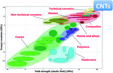 | ||
| Fig. 2 Ashby plot showing Young's modulus plotted against tensile strength for many engineering materials. Based on theoretical calculations and experimental measurements, CNTs exhibit the highest Young's modulus and tensile strength.101 Plot made using the CES EduPack software, Granta Design Ltd., Cambridge, UK (http://www.grantadesign.com). | ||
The thermal properties of a suspended metallic SWCNT were extracted from high-bias (I–V) electrical characteristics achieved by Joule self-heating over the 300–800 K temperature range by Pop et al.14 They measured a thermal conductivity of almost 3500 W m−1 K−1 at room temperature for a 2.6 µm long SWCNT with a diameter of 1.7 nm and developed a model of thermal conductivity as a function of nanotube diameter and temperature. Similarly, Kim et al.15 measured a thermal conductivity above 3000 W m−1 K−1 at room temperature for multi-wall CNTs using a microfabricated suspended device.
These high values for thermal conductivity constitute another useful property for electrical applications as thermal management and dissipation have become a very critical issue for downscaling the dimensions of future microprocessors.
Given that the emitted current is strongly influenced by the emitter shape (geometric field enhancement) and by the chemical state of the surface, the small diameter and elongated shape of nanotubes lead to a high geometrical field enhancement making them ideal candidates for field emission applications such as displays or triodes.12,52,106–120
2. Synthesis of carbon nanotubes
Although hundreds of tons of CNTs are produced per year,121 the vast majority are substrate-free CNTs. A typical application is mechanical reinforcement where the CNTs are dispersed into polymeric matrices. This report will mostly focus on CNT synthesis on substrates, which is critical for most electronic applications.2.1 Grow-in-place vs. grow-then-place approach
To utilize carbon nanotubes on substrates in industrial applications, two main approaches have been considered: grow-in-place and grow-then-place (Fig. 3).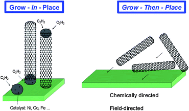 | ||
| Fig. 3 Pictorials comparing the “grow-in-place” and “grow-then-place” techniques.122 Figure reproduced with permission from Professor Carl V. Thompson (MIT). | ||
The advantages of this synthesis method include:
- knowledge, and in some cases control of nanotube position (CNTs will grow where there are catalyst dots)
- proven recipes to obtain carpets of vertically aligned crystalline CNTs (at least on insulating substrates)
- good physical and electrical contact with the substrate
- maturity of the used CVD techniques and experience of the complementary metal–oxide–semiconductor (CMOS) industry with CVD technology
The major drawback of the grow-in-place approach is the risk of damaging pre-existing structures during the synthesis. For instance, this is a major issue for implementation of nanotubes in the CMOS industry as any processing above 400–450 °C may disrupt previous diffusion patterns. Furthermore, to achieve electrical contact, the CNTs need to be synthesized on a metallic layer, which has proven challenging.
The advantages of this method include:
- no restrictions on the process or temperature used for CNT synthesis
- ability to pretreat CNTs (e.g., select, purify, functionalize)
The major drawback of the grow-then-place approach is the still insufficient level of repeatability and control to transfer the CNTs to specific regions of a substrate, which makes it an unlikely candidate for substrate-based applications (e.g., electronic devices).
2.2 Fabrication of substrate-free CNTs
A wide variety of fabrication methods have been used to synthesize carbon nanotubes. Techniques such as arc discharge and laser ablation allow synthesis of substrate-free CNTs with good crystallinity at high temperature. Although this review focuses mostly on thermal CVD, this brief section will introduce the reader to the most popular CNT fabrication methods to synthesize substrate-free CNTs and to the main post-processing techniques.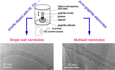 | ||
| Fig. 4 Schematics of an arc discharge apparatus, along with electron microscopy pictures of the products obtained with doped and pure anodes.130 Figure reproduced with permission from Dr Jean-Marc Bonard, École Polytechnique Fédérale de Lausanne (EPFL), Switzerland, http://ipn2.epfl.ch/CHBU/NTproduction1.htm. | ||
To synthesize nanotubes using this method, carbon electrodes are heated to high temperature in total absence of oxygen by electric current. If a catalyst is added to one of the electrodes, nanotubes can be obtained. The mechanism is based on energy transfer between the target materials (graphite), which is kept at temperatures close to its melting point, and an external radiation source (Fig. 4). The same mechanism applies to laser ablation.
The major advantage of this technique is that it is possible, by appropriately tuning the process parameters, to produce nanotubes with a very good degree of crystallinity, which leads to superior electrical and mechanical properties. This is due to the high temperature at which the process operates (above 2000 K), which is much higher compared to CVD. The major drawback is that the nanotubes have to be separated from other carbon products and catalyst residue.
Various metals can be used as catalysts: iron, nickel, cobalt, boron, etc. An inert gas such as helium or argon fills the chamber, which is kept at low pressure. After the arc is triggered, a plasma consisting of carbon, rare gases, and catalyst vapors is established between the electrodes, where a difference of potential is applied. The anode (graphite target doped with catalyst metal) is eroded during the process.
Among the variables that can be controlled to optimize the yield and the quality of this process, we can mention:
- type of doped anode (which can be homogeneously or heterogeneously doped)
- nature and concentration of catalysts
- gases composing the plasma
- inert gas pressure
- arc current intensity
- distance between the electrodes
By varying one or more of the above variables, we can obtain different carbon structures such as SWCNTs, MWCNTs, double-wall CNTs, C60, amorphous carbon, etc.131 Even when optimizing the process to synthesize nanotubes, bundles of CNTs are formed in the reactor, usually coated with a thin layer of amorphous carbon (2–5 nm) containing fullerenes. By replacing the graphite powder (sp2 hybridized carbon) with diamond powder (sp3 hybridized carbon) mixed with the catalyst powder, the yield of CNTs can be increased by 230%.131
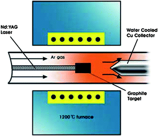 | ||
| Fig. 5 Schematics of laser ablation reactor (source: Eindhoven University of Technology133). Figure reproduced with permission from Professor Peter H. L. Notten, Philips Research Laboratories, http://students.chem.tue.nl/ifp03/synthesis.html. | ||
Among the laser beam parameters that can be tuned to optimize the output, we can mention:
- wavelength (for rapid and complete ablation, the wavelength chosen should lead to minimum absorption depth to ensure that all the energy is delivered in a small volume)
- short pulse duration (to maximize peak power and to minimize conduction loss to the surrounding environment)
- pulse repetition rate (should be rapid)
- beam quality (brightness, focusability, and homogeneity)
With this method, we can collect MWCNTs in the soot that are 1.5 nm to 3.5 nm in diameter and with length around 300 nm. Nanotube crystallinity is a function of the furnace temperature (1200 °C is optimal for best quality CNTs). By introducing small quantities of metal catalyst in the pellet, SWCNTs with good crystallinity can be obtained.
2.3 Post-processing techniques
Post-processing techniques are mostly applied to substrate-free CNTs and allow purification or alteration of the properties of the grown CNTs. Note that, although post-processing usually applies to substrate-free grown CNTs, some techniques can also be applied on CNTs grown on substrates using CVD. A selection of the most common post-processes will be illustrated here.Cap opening and removal of amorphous carbon from CNTs are processes that also apply to CVD growth to open the caps of carpets of VACNTs or to remove amorphous carbon from the nanotube sidewalls. It may be a critical step for devices and energy applications. By adding parts per million (ppm) of water vapor, Hata et al.19 obtained CNTs that did not show an amorphous coating on the external walls (in addition to maintaining the catalyst dots clear of amorphous carbon, thus delaying growth termination). Similarly, Zhu et al.134,135 used water to open the CNT caps and to clean the catalyst dots to restart CNT growth multiple times. Delpeux et al.136 used a two-step technique on CNTs not bound to substrates that opened the caps and cleaned the CNTs from debris.
Separation or selection is the process that allows selecting specific types of CNTs out of the total output. This can be applied to CNTs grown using CVD and subsequently peeled from the substrate to be used as additives in solution for conductive composites or electrodes for energy applications (batteries and supercapacitors). For instance, Krupke et al.137 separated metallic from semiconducting SWCNTs from a suspension using alternating current dielectrophoresis. The metallic and semiconducting SWCNTs move in opposite directions along the electric field gradient given that they present different relative dielectric constants with respect to the solvent.
Functionalization is the process of attaching groups of molecules to a surface to serve a specific purpose.138 Lee and Marzari139 used covalent functionalization to preserve or control the conductance of metallic SWCNTs. Using diazonium, Strano et al.140 functionalized SWCNTs suspended in aqueous solution leading to high selectivity, thus enabling manipulation to select the metallic tubes. Strano141 also separated SWCNTs of opposing chirality using centrifugation. Similarly, Campidelli et al.142 used covalent functionalization to separate metallic and semiconducting SWCNTs. Kong et al.143 functionalized CNTs with non-continuous Pd coating for molecular hydrogen sensors. By doping half length of a semiconducting SWCNT p-type and the other half n-type, Zhou et al.144 developed a pn junction. For the interested reader, the review from Tasis et al.145 describes chemical approaches to CNT functionalization.
Purification is the process of removing the impurities, namely catalyst particle, soot, and amorphous carbon from CNTs. For instance, Hou et al.146 discussed the purification of MWCNTs synthesized by the floating catalyst method using ultra-sonication, heat treatment in hot water, bromination, oxidation and acid treatment to remove most of the amorphous carbon, multishell carbon nanocapsules, and metal particles.
2.4 Chemical Vapor Deposition (CVD)
Chemical Vapor Deposition (CVD) allows grow-in-place synthesis of CNTs at lower temperatures compared to arc discharge and laser ablation, thus it is the most suitable candidate technique for CNT synthesis in the electronics and CMOS industry.121 CVD is already used in nano-electronics fabrication, exhibits high throughput, allows growth at relatively low temperatures (especially compared with laser ablation and arc discharge), and, most importantly, allows the grow-in-place approach for direct CNT growth on a substrate. Additionally, CVD can be integrated as a step in chip fabrication and, by following appropriate patterning steps, can be used to synthesize CNTs in desired locations on a substrate. A quick overview of CVD technology will follow, while the next section will analyze the various mechanisms and process parameters involved in this process.CNT synthesis by CVD is based on the catalytic decomposition of carbon-containing gases on catalysts, usually transition metals (Fe, Co, Ni) or alloys, in the form of thin films or as deposited nanoparticles. The growth temperature typically varies between 700 °C and 900 °C as high temperature is necessary for the catalysis to occur. Recent encouraging results have been obtained to reduce this temperature to values compatible with CMOS processes (400–450 °C).48,64,82 CNT catalysis can be heterogeneous (usually with a ferromagnetic thin film or nanoparticles as catalysts) or homogeneous (catalysis in the gas phase which contains the carbon gas and catalyst particles such as ferrocene). CVD usually allows synthesis of longer CNTs147 (up to centimetres) but with more defects compared to higher temperature processes such as laser ablation and gas discharge, although a post-annealing process at temperatures close to 2000 °C may recover the crystalline structure.148
The CVD process is based on using an energy source (e.g., a furnace with resistive or inductive heater (Fig. 6), hot filament, infra-red lamp, etc.) to decompose the precursor gases (gas decomposition) and to heat the sample (CNT nucleation and growth). In thermal CVD, the heat of the furnace is responsible for the decomposition of the precursor gases in addition to affecting the catalytic function of the substrate. Other CVD systems such as plasma-enhanced CVD (PECVD) use plasma to aid the gas decomposition, which often allows CNT growth at lower temperatures although it produces defects in the nanotube structure (Fig. 7).
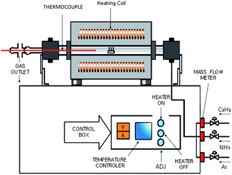 | ||
| Fig. 6 Schematic diagram of thermal CVD apparatus (source: Eindhoven University of Technology133). Figure reproduced with permission from Professor Peter H. L. Notten, Philips Research Laboratories, http://students.chem.tue.nl/ifp03/synthesis.html. | ||
 | ||
| Fig. 7 Schematic diagram of plasma CVD apparatus (source: Eindhoven University of Technology133). Figure reproduced with permission from Professor Peter H. L. Notten, Philips Research Laboratories, http://students.chem.tue.nl/ifp03/synthesis.html. | ||
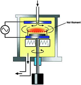
An interesting variant is hot-filament CVD, where a hot filament heats the gases to high temperature in close proximity to the sample. For instance, Jeong et al.149 used a hot filament CVD system (in addition to a Pd layer (dual catalyst) in close proximity to the sample) to grow carpets of VACNTs at 550 °C using Ni as a catalyst on a Si wafer (Fig. 8).
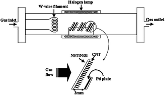 | ||
| Fig. 8 Schematic diagram of thermal CVD system designed for the CNT growth at low temperature. Note the Pd plate (dual catalyst) positioned a few mm across the sample.149 Figure reproduced with permission from: H. J. Jeong, S. Y. Jeong, Y. M. Shin, J. H. Han, S. C. Lim, S. J. Eum, C. W. Yang, N. G. Kim, C. Y. Park and Y. H. Lee, Chem. Phys. Lett., 2002, 361, 189–195. Copyright 2002, Elsevier. | ||
The HiPCO process (high pressure CO disproportionation process) is a CVD-based technique for catalytic production of SWCNTs in a continuous-flow gas phase using CO as the carbon feedstock and Fe(CO)5 as the iron-containing catalyst precursor. Although it generates substrate-free nanotubes, it has commercial interest because of its high SWCNT yield (above 70%) and because the diameter distribution of the SWCNTs, as small as 0.7 nm (average diameter 1.1 nm), can be tuned by controlling the pressure of CO (Fig. 9).150
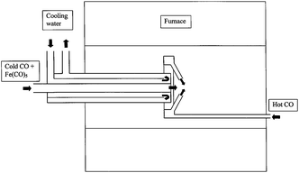 | ||
| Fig. 9 Layout of CO flow-tube reactor, showing water-cooled injector and ‘showerhead’ mixer.150 Figure reproduced with permission from: P. Nikolaev, M. J. Bronikowski, R. K. Bradley, F. Rohmund, D. T. Colbert, K. A. Smith and R. E. Smalley, Chem. Phys. Lett., 1999, 313, 91–97. Copyright 1999, Elsevier. | ||
Table 1 provides a quick comparison of selected parameters for the three major fabrication methods described.8
| Method | Operating temperature/°C | CNT length/µm | CNT growth rate/µm s−1 | Yield | Quality | Purity |
|---|---|---|---|---|---|---|
| Arc discharge | ∼4000 | ∼1 | up to 107 | Low | Low | Low |
| Laser ablation | Room temperature to 1000 | ∼1 | ∼0.1 | Low | High | Medium |
| Thermal CVD | 500–1200 | 0.1 to 105 | 0.1–10 | High | Medium | Medium to high |
| PECVD | 100–800 | 0.1–10 | 0.01–1 | Low | Low–medium | Medium |
3. Synthesis of CNTs on substrates using thermal CVD
Chemical vapor deposition is regarded as one of the most promising manufacturing techniques to be scaled to industrial production,121,151 especially if the nanotubes need to be grown on a substrate, as it is most often the case for electronic applications. Note that CVD techniques have also been efficiently used to produce large yields of substrate-free CNTs (e.g., fluidized-bed reactors152–154). The complexity of CNT synthesis is due to the large array of parameters that affect the outcome of the synthesis, mainly in the aspect of materials and processes, and to our still incomplete understanding of the CNT growth mechanisms. Materials choices include catalyst, underlayer, substrates, dual catalyst plates, etc. The complete process requires consideration of gases (mix, flow rates, reducing agents, oxidizing agents, hydrocarbons, etc.) and temperatures (substrate, gas, thermal profile, etc.) for each process step (annealing, growth, post-growth, etc.). Additionally, reactor technology (tube furnace, substrate heater, etc.), and duration of the various steps will affect the outcome.After Iijima opened the field of carbon nanotube research with his 1991 paper,26 in the 15 years that followed scientists published thousands of papers describing “recipes” on how to grow CNTs by varying the catalyst materials, the processing gases, the thermal process, etc. Although a majority of papers did not present significant discussion of mechanisms, they were still published as CNT growth by itself was challenging and could be regarded as an art. In recent years, publications more likely included significant insights on the growth mechanisms and sophisticated characterizations highlighting the structure of the CNTs. To illustrate the complexity of the task, Fig. 10 reproduced from Melechko et al.155 shows the vast disparity in growth output obtained by varying just two parameters such as the temperature and the ratio of hydrocarbon gas (C2H2) to reducing gas (NH3).
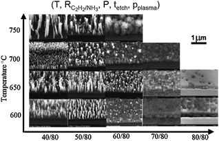 | ||
| Fig. 10 Carbon nanofibers grown from 10 nm of NiFe alloy (50% : 50%) on 10 nm Ti buffer layer by varying growth temperature and ratio of hydrocarbon gas to reducing gas.155 Figure reproduced with permission from: A. V. Melechko, V. I. Merkulov, T. E. McKnight, M. A. Guillorn, K. L. Klein, D. H. Lowndes and M. L. Simpson, J. Appl. Phys., 2005, 97, 041301. Copyright 2005 American Institute of Physics. | ||
This section will review different aspects of our current understanding of the CNT growth mechanism using thermal CVD. After reviewing general insights on the synthesis of CNTs, specific areas such as the roles of catalyst and underlayer,† CNT nucleation and growth, the role of gases, and some post-processing techniques will be described using examples from recent research.‡ The section will conclude with a brief review of some interesting technical variations of the reactor technology that could enhance future CNT synthesis and in situ characterization.
3.1 Insights into CNT growth mechanisms
The growth mechanism of carbon nanotubes is still not clearly understood although extensive experimental and theoretical studies, and, more recently, in situ HRTEM have provided numerous hints on the possible mechanisms at play. As of today, it is still an art to select the right materials and process parameters to grow the desired CNTs.The most accepted growth model is the vapor–solid–solid (VSS) model which derives from the vapor–liquid–solid (VLS) model originally suggested by Wagner and Ellis156 for growth of silicon whiskers. Using the VSS model, the excess carbon from the decomposition of the hydrocarbon gases precipitates on the surface of the catalyst, diffuses into the catalyst, and nucleates the nanotube at the edges of the catalyst.
For catalysts on a substrate, two main growth models have been reported:
- tip-growth, where the nanotube lifts the catalyst from the substrate during the growth, as the nanotube nucleates and grows below the catalyst
- base-growth, where the nanotube nucleates and grows above the catalyst, which remains attached to the substrate
Note that some teams claim growth models that combine tip and base growth, usually achieved by the presence of more than one catalyst dot during growth.157–159
Figure 11 depicts possible mechanisms from two groups who have made significant contributions to the understanding of CNT growth: Hofmann et al.160 who model tip-growth and Puretzky et al.161 who model base-growth. Although the relative simplicity of the models just described is deceptive as a wide variety of parameters, all inter-related, are critical for the successful synthesis of CNTs, the base-growth162–164 and tip-growth165,166 mechanisms have been observed using in situ HRTEM techniques.163–165,226,245
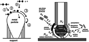 | ||
| Fig. 11 Popular models of carbon nanotube growth mechanism (sources: Hofmann et al.160 (left) and Puretzky et al.161 (right)). Figure on the left reprinted with permission from: S. Hofmann, G. Csanyi, A. C. Ferrari, M. C. Payne and J. Robertson, Phys. Rev. Lett., 2005, 95, 3. http://prl.aps.org/abstract/PRL/v95/i3/e036101, Copyright 2005 by the American Physical Society. Figure on the right reprinted with permission from: A. A. Puretzky, D. B. Geohegan, S. Jesse, I. N. Ivanov and G. Eres, Appl. Phys. A: Mater. Sci. Process., 2005, 81, 223–240. Copyright 2005, Springer Berlin/Heidelberg. | ||
Which of the two mechanisms is favored during growth depends on the interactions between the catalyst and the substrate materials. Wang et al.167 observed tip-growth using Fe catalyst on SiO2 and base-growth using Fe on Ta; by measuring the contact angle of the catalyst dots with the substrates, they inferred that base-growth was at play when the surface energy of the Ta substrate was higher than the Fe/Ta interface, while tip-growth was at play when the surface energy of the SiO2 substrate was lower than the Fe/SiO2 interface (Fig. 12).
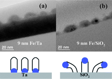 | ||
| Fig. 12 Comparison of CNT growth on Ta (base growth) and on silica (tip growth) using Fe catalyst.167 Figure adapted with permission from: Y. Y. Wang, B. Li, P. S. Ho, Z. Yao and L. Shi, Appl. Phys. Lett., 2006, 89, 183113. Copyright 2006 American Institute of Physics. | ||
As it is common to grow CNTs from catalyst and underlayer thin films (e-beam evaporated or sputtered onto a substrate), a critical mechanism is the way the catalyst thin film dewets to form the catalyst dots. Controlling the size of the catalyst dots is critical as this will influence the diameter and number of walls of the resulting CNTs.168,169 However, this task is extremely complex because of the interplay between catalyst and underlayer materials, catalyst layer thickness, gas atmosphere and thermal process, which will all influence the rates of dewetting and subsequent coarsening.
Extensive studies have been done using the catalyst–underlayer system of iron on alumina because it can yield dense carpets of VACNTs with large tolerance on the process parameters.19,170–173 Techniques such as controlled reduction and coarsening, engineering the catalyst layer thickness, etc. can help to control the outcome when growing CNTs on insulating substrates. Annealing or growing in a reducing gas atmosphere, typically hydrogen,172 ammonia,174,175 or hydrazine vapor173 can deoxidize the catalyst surface and accelerate catalyst migration, thus leading to larger catalyst dots, which lead to CNTs of larger diameter and increased number of walls. Nessim et al.172 showed that control of the reduction step leads to control of the catalyst dot size, which in turn controls the CNT diameter and number of walls. Additionally, Chhowalla et al.169 showed that a thicker catalyst layer generated larger catalyst dots, all other parameters being equal (Fig. 13).
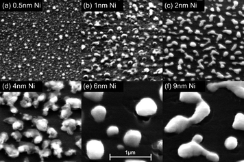 | ||
| Fig. 13 SEM photographs of Ni films with varying thicknesses deposited using magnetron sputtering on 50 nm of SiO2 after annealing at 750 °C in 20 Torr of H2 for 15 minutes (source: Chhowalla et al.169). Figure reproduced with permission from: M. Chhowalla, K. B. K. Teo, C. Ducati, N. L. Rupesinghe, G. A. J. Amaratunga, A. C. Ferrari, D. Roy, J. Robertson and W. I. Milne, J. Appl. Phys., 2001, 90, 5308–5317, Copyright 2001 American Institute of Physics. | ||
Growing CNTs on metallic underlayers is more difficult because alloying and increased mobilities hinder CNT nucleation and growth while inadequate dewetting/coarsening may lead to an insufficient density of catalyst dots. This usually results in entangled carbon nanotubes as opposed to carpets of VACNTs because of the insufficient steric hindrance from neighboring CNTs during growth.82,176 As will be described in the next sections, appropriate choice of the underlayer material and thermal process allows CNT growth on metallic layers.82,176
Although this review is mostly focused on using CVD to grow dense and tall carpets of VACNTs on substrates, there have been successful reports of horizontal growth of CNTs on substrates for transistors, sensors and other electronic devices. Vertical alignment during growth of vertical carpets of CNTs is usually attained when the density of the catalyst dots is high enough to engender steric hindrance between the CNTs, thus leading to vertically aligned growth. In the absence of steric hindrance individual nanotubes should be subjected to external forces to grow horizontally. Among the many possible techniques, the use of gas flow rate, electric field, and epitaxial techniques to guide horizontal alignment of the nanotubes will be discussed.
The group of Professor Liu20,177–179 at Duke university pioneered the growth of cm-long and horizontally aligned CNTs using the fast-heating technique where, by quickly heating the substrate, the CNT tips are lifted above the substrate. The gas flow then directed the growing CNTs suspended above the substrate in a “kite-mechanism”. Using a rotating substrate in situ during the CVD process, Hofmann et al.180 provided additional insights on the horizontal growth of CNTs aligned with the gas flow. They showed that the orientation of floating nanotubes with respect to the substrate is changed by interaction with the gas stream and that a vertical gas stream due to thermal buoyancy over the sample kept the nanotubes floating for extended times.
Professor Dai's group in Stanford181–183 demonstrated that electric fields significantly enhanced horizontal alignment of CNTs by inducing large dipole moments, which led to strong aligning torques and forces on the nanotubes, thus overcoming randomization of nanotube orientation by thermal fluctuations and gas flows. The challenge is that strong electric fields (0.5–2 V µm−1) are needed.
Leveraging the approach of using step edges to align electrodeposited nanowires,184 epitaxial approaches have been used to horizontally align CNTs. Among the various techniques, we can mention the surface-guided growth along lattice directions (lattice-directed epitaxy)185–187 and atomic steps (ledge-directed epitaxy)188,189 on single-crystal surfaces. The team of professor Joselevich at the Weizmann Institute (Israel) developed the graphoepitaxy technique, which consists of aligning CNTs along nanofacets (graphoepitaxy).190,191 Combining this technique with the use of an applied electric field, they were able to grow CNTs in a crossbar geometry.192
3.2 Catalyst and underlayer material choices
As thermal CVD of CNTs is a heterogeneous catalysis process, catalyst dots that will act as nucleation sites for CNT growth should be present to start the nucleation of CNTs. Since the catalyst will influence the resulting CNT growth, the catalyst dot can be considered as the “father” of the resulting nanotube. The catalyst material can be in the source gas (floating catalyst method193–195) or, more often, it is present on a substrate and represents the nucleation points. We will focus here on substrate-based catalysts because this technique allows catalyst patterning on the substrate196 (which will lead to CNT growth only on the pre-patterned areas) and also a higher level of control of catalyst density and size. The ferromagnetic metals, Fe,172,197–201 Co,28,196,202 and Ni,169,203,204 are the most used catalysts for CNT growth using thermal CVD205 although various teams have been able to synthesize CNTs using other metals,206–209 alloys,210,211 and, more recently, oxides.212 Alloys containing Mo deserve a special mention as it was shown to provide a stabilizing function to the catalyst even though Mo is considered inactive for CNT growth.151,211,213–216The catalysts are usually deposited on a substrate as a thin film using processes such as e-beam evaporation or sputtering, or are deposited as nanoparticles from solution (dipping or electrochemistry) or using specific apparatus (impactors65) or processes (e.g., particles templated by block copolymer micelles217) to control the mean particle size. For thin films, where the film dewets into catalyst dots during the thermal process, it was shown above that the thickness of the catalyst film is directly correlated to the final catalyst dot size, which in turn determines the CNT diameter.168,169 For catalyst nanoparticles,199 the nanoparticle size directly affects the nanotube diameter, assuming the thermal process does not affect the nanoparticle morphology.
The processes of dewetting/coarsening and CNT nucleation/growth are complex and often happen simultaneously. One way to decouple these two processes is to pretreat the catalyst layer. For instance, annealing in a reducing atmosphere without hydrocarbon gases can start the catalyst reduction, dewetting and coarsening without precipitation of carbon on the catalyst dot surface.172,173 Alternatively, the catalyst nanodots can be generated by plasma exposure174 of the surface prior to growth or through wet chemical etching. The schematic in Fig. 14171 illustrates the evolution from thin film to carbon nanotube carpet.
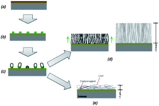 | ||
| Fig. 14 Schematic of CNT growth steps: (a) sample with thin film catalyst; (b) catalyst thin film dewetting and formation of catalyst dots; (c) CNT nucleation on catalyst dots; (d) high catalyst dots density leads to growth of tall carpet of VACNTs; (e) low catalyst dots density leads to entangled carpets of CNTs.171 Figure adapted with permission from Professor A. John Hart, Copyright 2006 Massachusetts Institute of Technology. | ||
The oxidation state of the catalyst during CNT nucleation is still a subject of debate because the catalyst may be active only for certain oxidation states. For instance, iron, one of the most widely used catalyst materials (usually on alumina or silicon oxide underlayers), can present up to sixteen oxidation states.218 Most reports agree that the catalyst dots are in their metallic state and that a reduction step prior to nucleation is needed172,173 although they may oxidize after the synthesis,200 while other indicated that oxidized dots are more efficient in nucleating CNTs.219 Experimental results using XRD220,221 or in situ HRTEM,166 which have been confirmed by molecular dynamics studies,222 indicated that intermediate metastable carbide phases may be present after the hydrocarbon gases are introduced.
An important question relates to the phase of the catalyst during CNT nucleation and growth. Although there is still debate about the catalyst state (liquid or solid), Harutyunyan et al.223,224 showed that the catalyst liquid phase favors the growth of CNTs, while the catalyst solid phase hinders it. This view is supported by the finding that the melting temperature of particles is dramatically reduced when their diameter fall below 100 nanometres in size.199,225
A related question is whether the catalyst crystallographic orientation influences nanotube nucleation and growth. In situ HRTEM observations by Rodriguez-Manzo et al.226 showed a relationship between the lattice spacing of the catalyst dot and the inter-distance between walls in a multi-wall CNT (0.34 nm) (Fig. 15). This finding hints to the importance of the crystallographic orientation of the catalyst during CNT nucleation and growth. Others supported a correlation between the crystallographic orientation of the catalyst and the resulting nanotubes,227–230 although these claims hint to the solid phase of the catalyst dots during nucleation and growth, which contrasts with the previously discussed claim that the catalyst is in the liquid phase.223,224,231
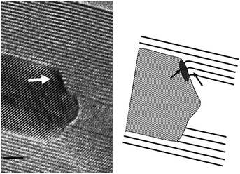 | ||
| Fig. 15 Interface between a FeCo crystal and a nanotube showing the relationship between the CNT walls and the catalyst crystallographic orientation.226 Figure reproduced with permission from: J. A. Rodriguez-Manzo, M. Terrones, H. Terrones, H. W. Kroto, L. T. Sun and F. Banhart, Nat. Nanotechnol., 2007, 2, 307–311. Copyright 2007 Nature Publishing Group. | ||
The interactions between catalyst and underlayer are numerous and complex. The choice of underlayer has proven extremely critical for CNT synthesis. For instance, CNTs have been grown successfully on insulating substrates by many teams worldwide that have developed a large number of successful recipes using various source gases and process conditions. This is in contrast with CNT synthesis on conductive layers which has proved much more difficult, as testified by the few publications on the topic.
Silicon oxide,232 magnesium oxide,233,234 and aluminium oxide19,235,236 are among the most popular underlayer materials for CNT growth. Iron catalyst on alumina underlayer has become the materials system of choice since Hata et al.19 successfully synthesized millimetre-tall, vertically aligned carpets of crystalline SWCNTs with iron catalyst on alumina underlayer by adding parts per million (ppm) of water vapor as a mild oxidizer.172,173,236–240
Growth on conductive underlayers is critical for electronic applications because they most often require electrical contact between the CNTs and the substrate upon which they are grown. However, this presents additional challenges because of the increased kinetic interactions such as alloying and formation of intermetallic compounds between catalyst and underlayer materials at the growth temperatures usually used for CNT growth on insulating layers (700–900 °C), thus making it critical to reduce the thermal dose. Although some have been successful by appropriately choosing specific underlayer materials such as Inconel,70,241 simply reducing the growth temperature usually does not work because the catalysis (CNT nucleation and growth) is inhibited. Awano et al.65 synthesized carpets of MWCNTs on Ti and TiN layers at 510 °C by depositing controlled-size Co nanoparticles using a custom-designed particle generator (impactor). A follow-up work by Yokoyama et al.64 achieved a similar result at a temperature of 400 °C. Nessim et al.82 synthesized dense carpets of VACNTs on Ta layers at temperatures approaching 500 °C by preheating the incoming gases at higher temperature (up to 770 °C). In addition to the materials properties, also the thickness of the underlayer has been found to critically influence the CNT growth. Delzeit et al.210 could grow CNTs on 20 nm thick Ir layers but growth did not occur when the thickness of the Ir layer was reduced to 5 nm or increased to 40 nm. Delzeit et al.242 also showed the influence of the thickness of the Al underlayer on CNT growth using Ni catalyst. Burt et al.243 found an optimum range of temperatures leading to CNT growth by analyzing the microstructure evolution of the Al underlayer. Nessim et al.176 showed how the melting temperature and the thickness of the underlayer influence CNT growth by comparing growth on Ta and Pd layers for varying thicknesses.
3.3 Nanotube nucleation and growth
The initial nucleation stage, where the carbon species diffuse into the catalyst dots and start CNT growth, is extremely complex as its kinetics is very fast (milliseconds)244 and difficult to observe. Recently, there have been interesting studies of nucleation using in situ HRTEM.163–165,226,245 A possible interpretation of the mechanisms is presented below based on a composite analysis of various studies, before delving into the gases and process parameters.Smalley and Dai et al.246 proposed the “yarmulke” model of MWCNT growth where the carbon compounds arriving at the catalyst surface initially assemble into a graphene cap, eliminating energetically expensive dangling bonds, thus reducing the catalyst surface energy. Once the first dome is formed on top of the catalyst dot, additional caps will form underneath in the case of MWCNTs. Finally, the cylindrical part of the CNT will grow. This model has been validated by in situ162,226 and isotope labelling247 experiments as well as by ab initio simulations (Fig. 16 and 17).229,248–250
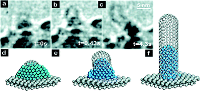 | ||
| Fig. 16 In situ HRTEM images and depictions of initial stages of CNT nucleation.162 Reproduced with permission from: S. Hofmann, R. Sharma, C. Ducati, G. Du, C. Mattevi, C. Cepek, M. Cantoro, S. Pisana, A. Parvez, F. Cervantes-Sodi, A. C. Ferrari, R. Dunin-Borkowski, S. Lizzit, L. Petaccia, A. Goldoni and J. Robertson, Nano Lett., 2007, 7, 602–608. Copyright 2007 American Chemical Society. | ||
 | ||
| Fig. 17 Ab initio simulations of the early stages of SWCNT growth on a 1 nm Fe catalyst.248 Figure reprinted with permission from J. Y. Raty, F. Gygi and G. Galli, Phys. Rev. Lett., 2005, 95, 9. http://prl.aps.org/abstract/PRL/v95/i9/e096103, Copyright 2005 by the American Physical Society. | ||
The structure of a crystalline cap is similar to the structure of a (half) fullerene. Pope et al.251 described a kinetic mechanism of fullerene formation based on the growth of polycyclic aromatic hydrocarbons (PAHs) and subsequent chemical reactions with hydrocarbons. Using the Pope model, Eres et al.252 hypothesized the cap formation as starting from PAHs such as fluoranthene, followed by stepwise addition of acetylene. For SWCNTs, once the cap was formed, the CNT wall started to grow thus lifting the cap.
3.4 Gases
Ethylene19,170,172,201,236,237,253 is probably the most popular hydrocarbon gas used in CNT synthesis although some synthesize CNTs using methane171,227,233 or acetylene173,238 (especially in PECVD). Others have used CO,213 alcohol,254,255 benzene256 or other gases or gas mixtures. Since Hata et al.19 showed that adding ppm of water vapor as a mild oxidizer led to VACNTs, there has been an increased focus on the role of reducing and oxidizing agents in the gas mix.18,172,197,202,232,233,257During nucleation and growth, gas species and thermal processes play a major role. The mechanisms at play are extremely complex and poorly understood as, at the moment where nucleation and growth occur, the hydrocarbon gas has dissociated into multiple species,258,259 including hydrogen, volatile organic compounds (VOCs), and larger polycyclic aromatic hydrocarbons (PAHs). The challenge is to characterize which gases contribute to CNT nucleation and growth and which gases inhibit growth.
If we follow the gas evolution from the gas tank, to the furnace, to the catalyst surface, and finally to the exhaust, we can map the following steps:
1. Fresh gas introduced from the gas tank into the furnace
2. Gas decomposition in the tube furnace at high temperature
3. Adsorption of gas species on the catalyst dots
4. Diffusion of carbon species into or on the catalyst dots and CNT nucleation and growth
5. Desorption of the gas species from the catalyst dots to the exhaust
The biggest challenge is to recognize which intermediate species adsorb onto the catalyst dots, which species diffuse into or on the catalyst, and which species may be responsible for terminating the reaction by covering the active catalytic surface (catalyst poisoning).
La Cava et al.260 studied carbon deposition over metal catalysts starting from hydrocarbons and showed that there are multiple pathways and intermediate steps for the gas to decompose and to adsorb onto a catalytic surface (Fig. 18).
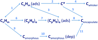 | ||
| Fig. 18 Alternative routes for the formation of carbon on metal catalysts showing the complexity of hydrocarbon decomposition.260 Examples of possible routes: A = 1, 2, and 4: (1) reversible adsorption of hydrocarbon, (2) dehydrogenation reactions on the surface, (4) to form a catalytic fibrous type of carbon (Cwhisker); B = 6, 7, and 8: (6 and 7) gas phase conversion of the hydrocarbon to form a polynuclear aromatic species, irreversibly adsorbed onto metallic sites of the surface, (8) surface rearrangement leading to encapsulating carbon; C = 9, 10, and 11: (9 and 10) formation of amorphous carbon in the gas phase, (11) dissolution and precipitation leading to encapsulating carbon. Reproduced with permission from: A. I. La Cava, C. A. Bernardo and D. L. Trimm, Carbon, 1982, 20, 219–223. Copyright 1982 Elsevier. | ||
In this analysis, pathway A (1 → 2 → 4) leads to the growth of fibrous carbon without loss of active metal using acetylene and olefins in the presence of high partial pressures of hydrogen. Pathway B (6 → 7 → 8) leads to the deactivation of the catalytic surface via carbon deposition on its surface. At high temperature, catalyst deactivation can be prevented by increasing the amount of hydrogen, thus leading to the reverse reaction path (3). The complexity of gas decomposition and its role in CNT synthesis have been highlighted by recent work on the role of gas preheating for CNT growth, where the exhaust gases were analyzed using gas chromatography/mass spectrometry (GC/MS). A large variety of gas compounds were detected, which hinted to the complexity of gas decomposition and the catalysis of CNTs.261,262
The pretreatment of the gases prior to their reaching the catalyst dot has recently been shown to be a critical step. Early reports indicated an improved CNT synthesis by using some form of preheating of the gases using hot-filament CVD263 or other forms of preheating.264,265 The key underlying mechanism is that the hydrocarbon gases decompose into a variety of compounds.266 Plata et al.261 showed that ethylene decomposed into multiple volatile organic compounds (VOCs) and many polycyclic aromatic hydrocarbons (PAHs). Using molecular beam-controlled nucleation and growth of CNTs, Eres et al.252 indicated an important role for fluoranthene. Meshot et al.262 showed how decoupling the gas preheat temperature from the substrate temperature allowed a better selection of process parameters for CNT growth. Nessim et al.82 preheated source gases to lower the substrate temperature when growing CNTs on metallic underlayers (Fig. 19).
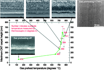 | ||
| Fig. 19 Plot showing the evolution of CNT carpet height as a function of gas preheat temperature and selected SEM images of CNT carpets grown with substrate zone set at 475 °C for different gas preheat temperatures. The HRTEM image on the top right shows the crystalline structure obtained when gas preheating is set to 770 °C.82 Reproduced with permission from: G. D. Nessim, M. Seita, K. P. O'Brien, A. J. Hart, R. K. Bonaparte, R. R. Mitchell and C. V. Thompson, Nano Lett., 2009, 9, 3398–3405. Copyright 2009 American Chemical Society. | ||
The last stage of gas decomposition/adsorption, namely catalyst poisoning which terminates CNT growth, has been analyzed by many teams. Zhu et al.134,135 claim that, as CNT carpets grow taller, the kinetics of diffusion of carbon species to the catalyst dots becomes more difficult until the growth stops. Han et al.267 proposed that a mechanical coupling of the top surface of the film hinders the relative movement of the CNTs in the carpet thus terminating growth. The most accepted theory is that amorphous carbon forms on top of the catalyst dots and prevents further diffusion, thus poisoning the catalysts and terminating CNT growth. Hata et al.19,170,237 and Pint et al.268 have successfully grown mm tall carpets of VACNTs by adding ppm of water (in parts per million) as a mild oxidizer to keep removing the amorphous carbon from the catalyst surface, thus extending the kinetics of CNT growth. Although the mechanisms at play are not clear, using ex situ microscopic and spectroscopic analysis, Yamada et al.240 showed that the catalyst was deactivated by carbon covering the catalyst dots and that the water kept the catalyst clean by ongoing removal of this coating. However, Amama et al.197 proposed that the water inhibited Ostwald ripening because of the ability of oxygen and hydroxyl species to reduce diffusion rates of catalyst atoms. Given the low packing density of carbon nanotubes, even for “dense” carpets where density does not exceed 1012 CNTs per cm2 (e.g. Awano et al.65), it is unlikely that diffusion through the CNT mass is the terminating step for nanotube growth, all the more so for entangled nanotube mats where densities are much lower. It is more likely that a chemical mechanism such as covering the catalyst surface with an amorphous coating is the terminating step (catalyst poisoning).
3.5 Innovative reactor design and in situ characterization
Despite the remarkable scientific progress achieved in CNT synthesis, the understanding of the underlying growth mechanisms remains incomplete. Further improvements to our understanding of these mechanisms could lead to better control of the CNT synthesis, which might entice the electronic and CMOS industry to invest in industrial fabrication for microprocessor elements (e.g., interconnects, CMOS transistor channels) and for future device electronics (e.g., sensors, field effect displays). In this respect, I believe that innovative reactor design and in situ characterization of CNT growth are two areas of investigation that can significantly contribute to achieve full control of reliable and repeatable CNT synthesis.A major issue preventing commercialization is the ability to develop repeatable processes. Although not explicitly discussed in the scientific literature, being able to consistently obtain the same CNT structures using the same CVD-based process parameters poses a challenge. For instance, researchers have observed that contamination of the quartz tube of the furnace can significantly influence the CNT growth.269
Most thermal CVD-based CNT growth experiments have been performed using single-zone tube furnaces. As previously discussed, the ability to decouple the preheating of the source gases from the heating of the sample can be extremely beneficial, especially for CNT synthesis on metallic layers.82 Many techniques can be used to decouple the gas preheat from the catalysis at the surface of the sample such as hot filament,263,270 remote plasma,64 or use of an additional heater262 (or a separate zone of a multi-zone tube furnace82,264) positioned in a way that the gases flow into a hot zone before reaching the sample.
One insufficiently studied topic related to the control of the gas atmosphere is the role of oxygen during the CNT growth.232 In addition to potentially oxidizing the catalyst and underlayer, oxygen impurities may influence the catalysis. Industrial settings use gettering furnaces271 to reduce the presence of oxygen in the reactor as much as possible. Another possible approach is to use low-pressure CVD, as it is currently used in PECVD systems.272
Veering away from the classic tube furnace design, Van Laake et al.273 developed an innovative cold-walled reactor in which a silicon strip serves as a substrate heater using resistive heat. When a high current is circulated into the silicon heater, its temperature increases very quickly allowing a reduction of the thermal dose and faster experimentation compared to standard tube furnaces. Cold-walled reactors are especially interesting because there is no concern about the influence of quartz tube contamination on CNT growth, which is often experienced on hot-walled reactors.269
A related area of research is the study of the influence of specific materials positioned in proximity to the sample and their influence on the CNT growth. For instance, Jeong et al.263 observed that a palladium plate positioned a few millimetres above the sample where CNTs were synthesized improved the CNT output. Positioning a material at high temperature in close proximity to the sample may significantly interact with the surrounding gases and influence their decomposition or recombination, thus affecting nanotubes' growth and structure.
The application of external fields is another possible area for further investigation. For instance, as previously discussed, horizontal alignment of CNTs was significantly enhanced by the application of local electrical fields.181 Using DC PECVD, AuBuchon et al.274,275 grew bent CNTs (L-shaped) by changing the direction of the electric field. Plasmas have shown significant effects on the pretreatment of catalyst layers and on the synthesis of CNTs, in addition to enhancing vertical alignment.160,169,174,276 How strong externally applied electric or magnetic fields with different orientations and intensities could affect CNT growth remains a largely unexplored area.
In parallel to innovative reactor designs that could enhance the output of CNT synthesis, in situ monitoring capabilities could significantly add to our understanding of the mechanisms of CNT growth. Although ex situ analyses are usually easier to implement, the information they provide might not reflect what truly happened during CNT nucleation and growth. For instance, ex situ XPS analysis of catalyst materials to determine their oxidation state may not be useful since the catalyst oxidizes upon exposure to the ambient atmosphere. Ex situ analysis of the exhaust gases has provided important information on the types of compounds that were present in the reactor, especially when focusing on the role of gas preheat.261,262 However, other important compounds may not have been detected because of interactions (e.g., adsorption) with the reactor walls or the steel canisters used to collect the gases.
As in situ techniques have historically accelerated the progress in synthesizing many advanced materials, including carbon nanotubes, there are still specific areas where they could critically contribute to augment our understanding of the CNT synthesis. At the simplest level, monitoring the evolution of nanotube morphology as a function of time and process parameters is relatively easy and can provide useful insights. Probing the structure of the catalyst–underlayer or of the CNTs in real-time as a function of process parameters poses challenges but is where the biggest opportunity lies to uncover new growth mechanisms.
To measure the height as a function of time of a growing CNT carpet, Van Laake et al. and Hart et al.273,277 used a laser system; they also filmed the growth using a high quality camera (the reactor was enclosed in a transparent glass enclosure). Alternative ways to measure the CNT carpet height in real-time during growth included using in situ optical absorbance measurements278,279 or time-resolved reflectivity of a HeNe laser beam.161,280
Multiple techniques allow in situ characterization of the evolving microstructure of the catalysts and nanotubes. Using Raman imaging to characterize the CVD growth of CNTs in situ and in real-time, Kaminska et al.281,282 detected single CNTs up to very high temperatures. With this technique, they observed the morphological evolution and the Raman spectra, the latter indicating the level of crystallinity and the diameter of SWCNTs. Van Laake et al.283 positioned their substrate-heater reactor in X-ray equipment and observed the catalyst thin film evolution in real-time using low angle X-ray scattering. In situ X-ray photoelectron spectroscopy198,212 (XPS) experiments provided critical information about the evolution of the composition and oxidation state of the catalysts during nucleation and growth. The most impressive characterization technique consists of growing CNTs inside a HRTEM allowing observation of the morphological evolution of both the microstructure of the catalysts and the nanotubes during nucleation and growth.163–165,226,245
4. Conclusions and outlook
Despite the array of impressive properties exhibited by CNTs (at least in theory) and the many devices that have been developed in the research labs, the overall picture that emerges from analyzing the complexity of CNT synthesis is that fabrication remains the key obstacle to make carbon nanotubes a commercial reality. The interrelated effects of the many parameters involved during CVD of CNTs account for the complexity of the task. Each synthesis requires a careful analysis of the properties of: (1) catalyst and underlayer materials; (2) the gas mix; (3) the effect of pretreatment on source gases; (4) the gas and substrate temperatures; and many other process parameters. In situ characterization techniques and new reactor designs should be carefully considered with the focus on uncovering the physical mechanisms under study and consistent with the CNT structure sought. Overall, a more complete understanding of CNT nucleation, growth, and termination may allow improvement of the synthesis to the level required for industrial applications.There is hope for commercialization, as many pieces of this incomplete puzzle have emerged in recent years. Many mechanisms have been identified through clever experiments and sophisticated in situ and ex situ characterizations. Some progress has been made on the analysis of the gas chemistry and on its interaction with the catalytic materials. New CVD reactors have been developed and have enabled additional mechanistic studies. Although a “unified” theory of CNT growth may not be achieved, additional studies of the interactions between gases, catalysts, and underlayers based on established materials science principles and coupled with sophisticated characterization equipment may pave the way to a more complete understanding of the growth mechanisms. Finally, more elaborate reactor designs may bridge the gap between the lab and the fab.
Acknowledgements
I want to acknowledge my PhD advisor and scientific mentor, Professor Carl V. Thompson (MIT) and many collaborators with whom I was privileged to work and from whom I learned a lot about CNTs, among whom I would mention Professors Jing Kong (MIT), Sam Allen (MIT), Brian Wardle (MIT), and John Hart (U. Mich), Dr Kevin O'Brien (Intel), Matteo Seita (ETH) and Donatello Acquaviva (EPFL). I acknowledge useful feedback on this report from Professors Carl Thompson and John Hart, and from Mario Hofmann (MIT), Alfonso Reina (MIT), and Donatello Acquaviva.Notes and references
- R. Saito, G. Dresselhaus and M. S. Dresselhaus, Physical Properties of Carbon Nanotubes, Imperial College Press, London, 1998 Search PubMed.
- Carbon Nanotubes: Synthesis, Structure, Properties, and Applications, ed. M. S. Dresselhaus, G. Dresselhaus and P. Avouris, Springer, Berlin, 2001 Search PubMed.
- M. Meyyappan, Carbon Nanotubes: Science and Applications, CRC Press, Boca Raton, FL, 2005 Search PubMed.
- S. Reich, C. Thomsen and J. Maultzsch, Carbon Nanotubes: Basic Concepts and Physical Properties, Wiley-VCH, Weinheim, Cambridge, 2004 Search PubMed.
- N. Abate, MSc thesis, Department of Electrical Engineering, Politecnico di Torino (research done at Massachusetts Institute of Technology), Torino, Italy, 2007.
- D. Acquaviva, MSc thesis, DMSE, MIT–Politecnico di Torino, INPG, EPFL, France, Switzerland, 2006, p. 151.
- G. D. Nessim, PhD thesis, Department of Materials Science and Engineering, Massachusetts Institute of Technology, Cambridge, MA, 2009, p. 336.
- M. Seita, MSc thesis, Department of Electrical Engineering, Politecnico di Torino (research done at Massachusetts Institute of Technology), Torino, Italy, 2007.
- J. P. Lu, Phys. Rev. Lett., 1997, 79, 1297–1300 CrossRef CAS.
- J. P. Salvetat, J. M. Bonard, N. H. Thomson, A. J. Kulik, L. Forro, W. Benoit and L. Zuppiroli, Appl. Phys. A: Mater. Sci. Process., 1999, 69, 255–260 CrossRef CAS.
- B. I. Yakobson, Appl. Phys. Lett., 1998, 72, 918–920 CrossRef.
- P. Avouris, J. Appenzeller, R. Martel and S. J. Wind, Proc. IEEE, 2003, 91, 1772–1784 CrossRef CAS.
- P. L. McEuen and J. Y. Park, MRS Bull., 2004, 29, 272–275 CAS.
- E. Pop, D. Mann, Q. Wang, K. Goodson and H. J. Dai, Nano Lett., 2006, 6, 96–100 CrossRef CAS.
- P. Kim, L. Shi, A. Majumdar and P. L. McEuen, Phys. Rev. Lett., 2001, 87, 215502 CrossRef CAS.
- A. López-Bezanilla, F. Triozon, S. Latil, X. Blase and S. Roche, Nano Lett., 2009, 9, 940–944 CrossRef CAS.
- B. Kozinsky and N. Marzari, Phys. Rev. Lett., 2006, 96, 166801–166804 CrossRef.
- Y. H. Yun, V. Shanov, Y. Tu, S. Subramaniam and M. J. Schulz, J. Phys. Chem. B, 2006, 110, 23920–23925 CrossRef CAS.
- K. Hata, D. N. Futaba, K. Mizuno, T. Namai, M. Yumura and S. Iijima, Science, 2004, 306, 1362–1364 CrossRef CAS.
- S. Huang, M. Woodson, R. Smalley and J. Liu, Nano Lett., 2004, 4, 1025–1028 CrossRef CAS.
- M. Reibold, P. Paufler, A. A. Levin, W. Kochmann, N. Patzke and D. C. Meyer, Nature, 2006, 444, 286–286 CrossRef CAS.
- M. Monthioux and V. L. Kuznetsov, Carbon, 2006, 44, 1621–1623 CrossRef CAS.
- T. V. Hughes and C. R. Chambers, USA, 405, 480, 1889.
- A. Oberlin, M. Endo and T. Koyama, J. Cryst. Growth, 1976, 32, 335–349 CrossRef CAS.
- A. Oberlin, M. Endo and T. Koyama, Carbon, 1976, 14, 133–135 CrossRef CAS.
- S. Iijima, Nature, 1991, 354, 56–58 CrossRef CAS.
- Wikipedia.
- D. S. Bethune, C. H. Kiang, M. S. Devries, G. Gorman, R. Savoy, J. Vazquez and R. Beyers, Nature, 1993, 363, 605–607 CrossRef CAS.
- S. Iijima and T. Ichihashi, Nature, 1993, 363, 603–605 CrossRef CAS.
- Tests Verify Carbon Nanotube Enable Ultra High Performance Transistor, NEC, 2003, http://www.nec.co.jp/press/en/0309/1901.html.
- J. Q. Wei, H. W. Zhu, D. H. Wu and B. Q. Wei, Appl. Phys. Lett., 2004, 84, 4869–4871 CrossRef CAS.
- Carbon nanotubes used in computer and TV screens, New Sci, 2005, 28, http://www.newscientist.com/article/mg18625006.800-carbon-nanotubes-used-in-computer-and-tv-screens-.html Search PubMed.
- The first computer circuit to be built on a single molecule has been unveiled by researchers in the US. http://news.bbc.co.uk/1/hi/sci/tech/4839088.stm, accessed 24 March, 2006.
- M. Kanellos, Carbon nanotubes enter Tour de France, http://news.cnet.com/Carbon-nanotubes-enter-Tour-de-France/2100-11395_3-6091347.html%3Ftag%3Dfd_carsl, accessed 7 July 2006.
- P. Marks, Optic nerve regrown with a nanofibre scaffold, New Sci., 2006, http://www.newscientist.com/article/dn8840-optic-nerve-regrown-with-a-nanofibre-scaffold-.html Search PubMed.
- A. P. Graham, G. S. Duesberg, W. Hoenlein, F. Kreupl, M. Liebau, R. Martin, B. Rajasekharan, W. Pamler, R. Seidel, W. Steinhoegl and E. Unger, Appl. Phys. A: Mater. Sci. Process., 2005, 80, 1141–1151 CrossRef CAS.
- H. Kataura, Y. Kumazawa, Y. Maniwa, I. Umezu, S. Suzuki, Y. Ohtsuka and Y. Achiba, Synth. Met., 1999, 103, 2555–2558 CrossRef CAS.
- Z. Xu, X. D. Bai, Z. L. Wang and E. G. Wang, J. Am. Chem. Soc., 2006, 128, 1052–1053 CrossRef CAS.
- H. W. Zhu, C. L. Xu, D. H. Wu, B. Q. Wei, R. Vajtai and P. M. Ajayan, Science, 2002, 296, 884–886 CrossRef CAS.
- The longest carbon nanotubes you've ever seen, http://www.nsf.gov/news/news_summ.jsp%3Fcntn_id%3D108992.
- M. S. Dresselhaus, G. Dresselhaus and P. Avouris, Carbon Nanotubes: Synthesis, Structure, Properties, and Applications, Springer, Berlin, New York, 2001 Search PubMed.
- W. Hoenlein, F. Kreupl, G. S. Duesberg, A. P. Graham, M. Liebau, R. Seidel and E. Unger, Mater. Sci. Eng., C, 2003, 23, 663–669 CrossRef.
- J. Bernholc, D. Brenner, M. B. Nardelli, V. Meunier and C. Roland, Annu. Rev. Mater. Res., 2002, 32, 347–375 CrossRef CAS.
- R. H. Baughman, A. A. Zakhidov and W. A. de Heer, Science, 2002, 297, 787–792 CrossRef CAS.
- S. Berber, Y.-K. Kwon and D. Tománek, Phys. Rev. Lett., 2000, 84, 4613 CrossRef CAS.
- T. Tong, Y. Zhao, L. Delzeit, A. Kashani, M. Meyyappan and A. Majumdar, IEEE Trans. Compon. Packag. Technol., 2007, 30, 92–100 CrossRef CAS.
- J. N. Coleman, U. Khan, W. J. Blau and Y. K. Gun'ko, Carbon, 2006, 44, 1624–1652 CrossRef CAS.
- M. Nihei, A. Kawabata, D. Kondo, M. Horibe, S. Sato and Y. Awano, Jpn. J. Appl. Phys., 2005, 44, 1626–1628 CrossRef CAS.
- E. J. Garcia, B. L. Wardle and A. J. Hart, Composites, Part A, 2008, 39, 1065–1070 CrossRef.
- P. Avouris, Acc. Chem. Res., 2002, 35, 1026–1034 CrossRef CAS.
- A. Naeemi and J. D. Meindl, IEEE Trans. Electron. Dev., 2007, 54, 26–37 CrossRef CAS.
- A. Di Carlo, A. Pecchia, E. Petrolati and C. Paoloni, in Nanomodeling II, SPIE, San Diego, CA, USA, 2006, pp. 632808–632811 Search PubMed.
- Y. Imry and R. Landauer, Rev. Mod. Phys., 1999, 71, S306–S312 CrossRef CAS.
- P. L. McEuen, M. Bockrath, D. H. Cobden, Y. G. Yoon and S. G. Louie, Phys. Rev. Lett., 1999, 83, 5098–5101 CrossRef CAS.
- J. Kong, E. Yenilmez, T. W. Tombler, W. Kim, H. J. Dai, R. B. Laughlin, L. Liu, C. S. Jayanthi and S. Y. Wu, Phys. Rev. Lett., 2001, 87, 106801 CrossRef CAS.
- M. Shiraishi and M. Ata, Carbon, 2001, 39, 1913–1917 CrossRef CAS.
- D. Mann, A. Javey, J. Kong, Q. Wang and H. J. Dai, Nano Lett., 2003, 3, 1541–1544 CrossRef CAS.
- H. Stahl, J. Appenzeller, R. Martel, P. Avouris and B. Lengeler, Phys. Rev. Lett., 2000, 85, 5186 CrossRef CAS.
- J. Kong, C. Zhou, A. Morpurgo, H. T. Soh, C. F. Quate, C. Marcus and H. Dai, Appl. Phys. A: Mater. Sci. Process., 1999, 69, 305–308 CrossRef CAS.
- C. W. Zhou, J. Kong and H. J. Dai, Appl. Phys. Lett., 2000, 76, 1597–1599 CrossRef CAS.
- C. W. Zhou, J. Kong and H. J. Dai, Phys. Rev. Lett., 2000, 84, 5604–5607 CrossRef CAS.
- H. T. Soh, C. F. Quate, A. F. Morpurgo, C. M. Marcus, J. Kong and H. J. Dai, Appl. Phys. Lett., 1999, 75, 627–629 CrossRef CAS.
- R. H. Baughman, C. Cui, A. A. Zakhidov, Z. Iqbal, J. N. Barisci, G. M. Spinks, G. W. Gordon, A. Mazzoldi, D. D. Rossi, A. G. Rinzler, O. Jaschinski, S. Roth and M. Kertesz, Science, 1999, 284, 1340–1344 CrossRef CAS.
- D. Yokoyama, T. Iwasaki, K. Ishimaru, S. Sato, T. Hyakushima, M. Nihei, Y. Awano and H. Kawarada, Jpn. J. Appl. Phys., 2008, 47, 1985–1990 CrossRef CAS.
- Y. Awano, S. Sato, D. Kondo, M. Ohfuti, A. Kawabata, M. Nihei and N. Yokoyama, Phys. Status Solidi A, 2006, 203, 3611–3616 CrossRef CAS.
- F. Chen, A. Joshi, V. Stojanović and A. Chandrakasan, Scaling and Evaluation of Carbon Nanotube Interconnects for VLSI Applications, in Nanonets Symposium 07, Catania, Italy, 2007 Search PubMed.
- F. Kreupl, A. P. Graham, G. S. Duesberg, W. Steinhogl, M. Liebau, E. Unger and W. Honlein, Microelectron. Eng., 2002, 64, 399–408 CrossRef CAS.
- J. Li, Q. Ye, A. Cassell, H. T. Ng, R. Stevens, J. Han and M. Meyyappan, Appl. Phys. Lett., 2003, 82, 2491–2493 CrossRef CAS.
- A. Naeemi and J. D. Meindl, IEEE Electron Device Lett., 2006, 27, 338–340 CrossRef.
- S. Talapatra, S. Kar, S. K. Pal, R. Vajtai, L. Ci, P. Victor, M. M. Shaijumon, S. Kaur, O. Nalamasu and P. M. Ajayan, Nat. Nanotechnol., 2006, 1, 112–116 CrossRef CAS.
- L. You, MSc thesis, Department of Electrical Engineering, Politecnico di Torino (research done at Massachusetts Institute of Technology), Torino, Italy, 2008.
- R. Martel, T. Schmidt, H. R. Shea, T. Hertel and P. Avouris, Appl. Phys. Lett., 1998, 73, 2447–2449 CrossRef CAS.
- A. Javey, J. Guo, Q. Wang, M. Lundstrom and H. J. Dai, Nature, 2003, 424, 654–657 CrossRef CAS.
- S. Heinze, J. Tersoff and P. Avouris, Appl. Phys. Lett., 2003, 83, 5038–5040 CrossRef CAS.
- S. Heinze, J. Tersoff, R. Martel, V. Derycke, J. Appenzeller and P. Avouris, Phys. Rev. Lett., 2002, 89, 106801 CrossRef CAS.
- A. Bachtold, P. Hadley, T. Nakanishi and C. Dekker, Science, 2001, 294, 1317–1320 CrossRef CAS.
- A. Bachtold, P. Hadley, T. Nakanishi and C. Dekker, Phys. E (Amsterdam, Neth.), 2003, 16, 42–46 Search PubMed.
- J. A. Misewich, R. Martel, P. Avouris, J. C. Tsang, S. Heinze and J. Tersoff, Science, 2003, 300, 783–786 CrossRef CAS.
- J. P. Clifford, D. L. John, L. C. Castro and D. L. Pulfrey, IEEE Trans. Nanotechnol., 2004, 3, 281–286 CrossRef.
- D. L. John, L. C. Castro, J. Clifford and D. L. Pulfrey, IEEE Trans. Nanotechnol., 2003, 2, 175–180 CrossRef.
- H. Kajiura, A. Nandyala and A. Bezryadin, Carbon, 2005, 43, 1317–1319 CrossRef CAS.
- G. D. Nessim, M. Seita, K. P. O'Brien, A. J. Hart, R. K. Bonaparte, R. R. Mitchell and C. V. Thompson, Nano Lett., 2009, 9, 3398–3405 CrossRef CAS.
- P. C. Collins, M. S. Arnold and P. Avouris, Science, 2001, 292, 706–709 CrossRef.
- P. G. Collins and P. Avouris, Appl. Phys. A: Mater. Sci. Process., 2002, 74, 329–332 CrossRef CAS.
- S. Frank, P. Poncharal, Z. L. Wang and W. A. de Heer, Science, 1998, 280, 1744–1746 CrossRef CAS.
- A. Bachtold, C. Strunk, J. P. Salvetat, J. M. Bonard, L. Forro, T. Nussbaumer and C. Schonenberger, Nature, 1999, 397, 673–675 CrossRef CAS.
- C. Schonenberger, A. Bachtold, C. Strunk, J. P. Salvetat and L. Forro, Appl. Phys. A: Mater. Sci. Process., 1999, 69, 283–295 CrossRef CAS.
- H. J. Li, W. G. Lu, J. J. Li, X. D. Bai and C. Z. Gu, Phys. Rev. Lett., 2005, 95, 086601 CrossRef CAS.
- M. F. Yu, B. S. Files, S. Arepalli and R. S. Ruoff, Phys. Rev. Lett., 2000, 84, 5552–5555 CrossRef CAS.
- A. Krishnan, E. Dujardin, T. W. Ebbesen, P. N. Yianilos and M. M. J. Treacy, Phys. Rev. B: Condens. Matter, 1998, 58, 14013–14019 CrossRef.
- G. Zhou, W. Duan and B. Gu, Chem. Phys. Lett., 2001, 333, 344–349 CrossRef CAS.
- Z. Yao, C.-C. Zhu, M. Cheng and J. Liu, Comput. Mater. Sci., 2001, 22, 180–184 CrossRef CAS.
- B. G. Demczyk, Y. M. Wang, J. Cumings, M. Hetman, W. Han, A. Zettl and R. O. Ritchie, Mater. Sci. Eng., A, 2002, 334, 173–178 CrossRef.
- E. J. Garcia, A. J. Hart, B. L. Wardle, A. H. Slocum and D. J. Shim, Aligned Carbon Nanotube Reinforcement Of Graphite/Epoxy Ply Interfaces, in 16th International Conference on Composite Materials, Kioto, Japan, 2007 Search PubMed.
- B. L. Wardle, D. S. Saito, E. J. García, A. J. Hart, R. Guzmán de Villoria and E. A. Verploegen, Adv. Mater., 2008, 20, 2707–2714 CrossRef CAS.
- A. K.-T. Lau and D. Hui, Composites, Part B, 2002, 33, 263–277 CrossRef.
- R. Ramasubramaniam, J. Chen and H. Liu, Appl. Phys. Lett., 2003, 83, 2928–2930 CrossRef CAS.
- J. K. W. Sandler, J. E. Kirk, I. A. Kinloch, M. S. P. Shaffer and A. H. Windle, Polymer, 2003, 44, 5893–5899 CrossRef CAS.
- E. T. Thostenson, Z. Ren and T.-W. Chou, Compos. Sci. Technol., 2001, 61, 1899–1912 CrossRef CAS.
- A. Trionfi, D. A. Scrymgeour, J. W. P. Hsu, M. J. Arlen, D. Tomlin, J. D. Jacobs, D. H. Wang, L. S. Tan and R. A. Vaia, J. Appl. Phys., 2008, 104, 083708–083706 CrossRef.
- M. F. Ashby, Materials Selection in Mechanical Design, Elsevier, 3rd edn, 2005 Search PubMed.
- J. Hone, Carbon Nanotubes, 2001, 80, 273–286 Search PubMed.
- J. Hone, M. Whitney and A. Zettl, Synth. Met., 1999, 103, 2498–2499 CrossRef CAS.
- W. Yi, L. Lu, Z. Dian-lin, Z. W. Pan and S. S. Xie, Phys. Rev. B: Condens. Matter Mater. Phys., 1999, 59, R9015 CrossRef CAS.
- R. H. Fowler and L. Nordheim, Proc. R. Soc. London, Ser. A, 1928, 119, 173–181 CrossRef.
- S. S. Fan, M. G. Chapline, N. R. Franklin, T. W. Tombler, A. M. Cassell and H. J. Dai, Science, 1999, 283, 512–514 CrossRef CAS.
- N. S. Lee, D. S. Chung, I. T. Han, J. H. Kang, Y. S. Choi, H. Y. Kim, S. H. Park, Y. W. Jin, W. K. Yi, M. J. Yun, J. E. Jung, C. J. Lee, J. H. You, S. H. Jo, C. G. Lee and J. M. Kim, Diamond Relat. Mater., 2001, 10, 265–270 CrossRef CAS.
- J. Li, C. Papadopoulos, J. M. Xu and M. Moskovits, Appl. Phys. Lett., 1999, 75, 367–369 CrossRef CAS.
- A. G. Rinzler, J. H. Hafner, P. Nikolaev, L. Lou, S. G. Kim, D. Tománek, P. Nordlander, D. T. Colbert and R. E. Smalley, Science, 1995, 269, 1550–1553 CrossRef CAS.
- J. M. Bonard, M. Croci, I. Arfaoui, O. Noury, D. Sarangi and A. Chatelain, Diamond Relat. Mater., 2002, 11, 763–768 CrossRef CAS.
- J. M. Bonard, M. Croci, C. Klinke, F. Conus, I. Arfaoui, T. Stockli and A. Chatelain, Phys. Rev. B: Condens. Matter Mater. Phys., 2003, 67, 085412 CrossRef.
- J. M. Bonard, F. Maier, T. Stockli, A. Chatelain, W. A. de Heer, J. P. Salvetat and L. Forro, Ultramicroscopy, 1998, 73, 7–15 CrossRef CAS.
- J. M. Bonard, J. P. Salvetat, T. Stockli, W. A. de Heer, L. Forro and A. Chatelain, Appl. Phys. Lett., 1998, 73, 918–920 CrossRef CAS.
- J. M. Bonard, J. P. Salvetat, T. Stockli, L. Forro and A. Chatelain, Appl. Phys. A: Mater. Sci. Process., 1999, 69, 245–254 CrossRef CAS.
- J. M. Bonard, T. Stockli, F. Maier, W. A. de Heer, A. Chatelain, J. P. Salvetat and L. Forro, Phys. Rev. Lett., 1998, 81, 1441–1444 CrossRef CAS.
- J. M. Bonard, T. Stockli, O. Noury and A. Chatelain, Appl. Phys. Lett., 2001, 78, 2775–2777 CrossRef CAS.
- J. M. Bonard, N. Weiss, H. Kind, T. Stockli, L. Forro, K. Kern and A. Chatelain, Adv. Mater., 2001, 13, 184–188 CrossRef CAS.
- W. A. deHeer, J. M. Bonard, K. Fauth, A. Chatelain, L. Forro and D. Ugarte, Adv. Mater., 1997, 9, 87–89 CrossRef CAS.
- W. A. deHeer, J. M. Bonard, T. Stockli, A. Chatelain, L. Forro and D. Ugarte, Z. Phys. D: At., Mol. Clusters, 1997, 40, 418–420 CrossRef CAS.
- W. A. Deheer, A. Chatelain and D. Ugarte, Science, 1995, 270, 1179–1180 CrossRef CAS.
- P. Eklund, A. Pulickel, R. Blackmon, A. J. Hart, J. Kong, P. Bhabendra, A. Rao and R. Rinzler, International Assessment of Research and Development on Carbon Nanotubes: Manufacturing and Applications, World Technology Evaluation Center, Baltimore, Maryland 21210, USA, 2007, http://www.wtec.org/cnm/.
- C. V. Thompson, in 46th International Reliability Symposium, IEEE CFP08RPS-PRT, Phoenix, Arizona, 2008, p. 368 Search PubMed.
- M. Ahlskog, E. Seynaeve, R. J. M. Vullers and C. Van Haesendonck, J. Appl. Phys., 1999, 85, 8432–8435 CrossRef CAS.
- J. Liu, M. J. Casavant, M. Cox, D. A. Walters, P. Boul, W. Lu, A. J. Rimberg, K. A. Smith, D. T. Colbert and R. E. Smalley, Chem. Phys. Lett., 1999, 303, 125–129 CrossRef CAS.
- R. Krupke, F. Hennrich, H. B. Weber, D. Beckmann, O. Hampe, S. Malik, M. M. Kappes and H. v. Löhneysen, Appl. Phys. A: Mater. Sci. Process., 2003, 76, 397–400 CrossRef CAS.
- M. Prashanth, S. Selvapraba, X. Xugang, C. Chia-Ling, B. Ahmed, K. Nishant and R. D. Mehmet, Nanotechnology, 2007, 395204.
- R. Krupke, F. Hennrich, H. B. Weber, M. M. Kappes and H. von Lohneysen, Nano Lett., 2003, 3, 1019–1023 CrossRef CAS.
- A. Vijayaraghavan, S. Blatt, D. Weissenberger, M. Oron-Carl, F. Hennrich, D. Gerthsen, H. Hahn and R. Krupke, Nano Lett., 2007, 7, 1556–1560 CrossRef CAS.
- B. I. Yakobson and R. E. Smalley, Am. Sci., 1997, 85, 324–337.
- L. G. Harrison, Trans. Faraday Soc., 1961, 57, 1191–1199 RSC.
- B. Bhushan, Springer Handbook of Nanotechnology, Springer, Berlin, New York, 2006 Search PubMed.
- T. Guo, P. Nikolaev, A. Thess, D. T. Colbert and R. E. Smalley, Chem. Phys. Lett., 1995, 243, 49–54 CrossRef CAS.
- M. J. M. Daenen, R. de Fouw, B. Hamers, P. G. A. Janssen, K. Schouteden and M. A. J. Veld, The Wondrous World of Carbon Nanotubes, a review on current carbon nanotube technologies, http://students.chem.tue.nl/ifp03/synthesis.html.
- L. B. Zhu, D. W. Hess and C. P. Wong, J. Phys. Chem. B, 2006, 110, 5445–5449 CrossRef CAS.
- L. B. Zhu, J. W. Xu, F. Xiao, H. J. Jiang, D. W. Hess and C. P. Wong, Carbon, 2007, 45, 344–348 CrossRef CAS.
- S. Delpeux, K. Szostak, E. Frackowiak and F. Beguin, Chem. Phys. Lett., 2005, 404, 374–378 CrossRef CAS.
- R. Krupke, F. Hennrich, H. v. Lohneysen and M. M. Kappes, Science, 2003, 301, 344–347 CrossRef CAS.
- B. Kannan and B. Marko, Small, 2005, 1, 180–192 CrossRef CAS.
- Y.-S. Lee and N. Marzari, Phys. Rev. Lett., 2006, 97, 116801–116804 CrossRef.
- M. S. Strano, C. A. Dyke, M. L. Usrey, P. W. Barone, M. J. Allen, H. Shan, C. Kittrell, R. H. Hauge, J. M. Tour and R. E. Smalley, Science, 2003, 301, 1519–1522 CrossRef CAS.
- M. S. Strano, Nat. Nanotechnol., 2007, 2, 340–341 CrossRef CAS.
- S. Campidelli, M. Meneghetti and M. Prato, Small, 2007, 3, 1672–1676 CrossRef CAS.
- J. Kong, M. G. Chapline and H. Dai, Adv. Mater., 2001, 13, 1384–1386 CrossRef CAS.
- C. Zhou, J. Kong, E. Yenilmez and H. Dai, Science, 2000, 290, 1552–1555 CrossRef CAS.
- D. Tasis, N. Tagmatarchis, A. Bianco and M. Prato, Chem. Rev., 2006, 106, 1105–1136 CrossRef CAS.
- P. X. Hou, S. Bai, Q. H. Yang, C. Liu and H. M. Cheng, Carbon, 2002, 40, 81–85 CrossRef CAS.
- S. Huang, M. Woodson, R. Smalley and J. Liu, Nano Lett., 2004, 4, 1025–1028 CrossRef CAS.
- M. Pinault, M. Mayne-L'Hermite, C. Reynaud, O. Beyssac, J. N. Rouzaud and C. Clinard, Diamond Relat. Mater., 2004, 13, 1266–1269 CrossRef CAS.
- H. J. Jeong, S. Y. Jeong, Y. M. Shin, J. H. Han, S. C. Lim, S. J. Eum, C. W. Yang, N.-g. Kim, C.-Y. Park and Y. H. Lee, Chem. Phys. Lett., 2002, 361, 189–195 CrossRef CAS.
- P. Nikolaev, M. J. Bronikowski, R. K. Bradley, F. Rohmund, D. T. Colbert, K. A. Smith and R. E. Smalley, Chem. Phys. Lett., 1999, 313, 91–97 CrossRef CAS.
- A. M. Cassell, J. A. Raymakers, J. Kong and H. J. Dai, J. Phys. Chem. B, 1999, 103, 6484–6492 CrossRef CAS.
- Y. Hao, Q. F. Zhang, F. Wei, W. Z. Qian and G. H. Luo, Carbon, 2003, 41, 2855–2863 CrossRef.
- Y. Wang, F. Wei, G. S. Gu and H. Yu, Phys. B, 2002, 323, 327–329 CrossRef CAS.
- Y. Wang, F. Wei, G. H. Luo, H. Yu and G. S. Gu, Chem. Phys. Lett., 2002, 364, 568–572 CrossRef CAS.
- A. V. Melechko, V. I. Merkulov, T. E. McKnight, M. A. Guillorn, K. L. Klein, D. H. Lowndes and M. L. Simpson, J. Appl. Phys., 2005, 97 Search PubMed.
- R. S. Wagner and W. C. Ellis, Appl. Phys. Lett., 1964, 4, 89–90 CAS.
- M. J. Height, J. B. Howard, J. W. Tester and J. B. V. Sande, J. Phys. Chem. B, 2005, 109, 12337–12346 CrossRef CAS.
- M. H. Kuang, Z. L. Wang, X. D. Bai, J. D. Guo and E. G. Wang, Appl. Phys. Lett., 2000, 76, 1255–1257 CrossRef CAS.
- Z. L. Wang and Z. C. Kang, Philos. Mag. B, 1996, 74, 51–69 CrossRef CAS.
- S. Hofmann, G. Csanyi, A. C. Ferrari, M. C. Payne and J. Robertson, Phys. Rev. Lett., 2005, 95, 036101 CrossRef CAS.
- A. A. Puretzky, D. B. Geohegan, S. Jesse, I. N. Ivanov and G. Eres, Appl. Phys. A: Mater. Sci. Process., 2005, 81, 223–240 CrossRef CAS.
- S. Hofmann, R. Sharma, C. Ducati, G. Du, C. Mattevi, C. Cepek, M. Cantoro, S. Pisana, A. Parvez, F. Cervantes-Sodi, A. C. Ferrari, R. Dunin-Borkowski, S. Lizzit, L. Petaccia, A. Goldoni and J. Robertson, Nano Lett., 2007, 7, 602–608 CrossRef CAS.
- M. Lin, J. P. Y. Tan, C. Boothroyd, K. P. Loh, E. S. Tok and Y. L. Foo, Nano Lett., 2006, 6, 449–452 CrossRef CAS.
- H. Yoshida, S. Takeda, T. Uchiyama, H. Kohno and Y. Homma, Nano Lett., 2008, 8, 2082–2086 CrossRef CAS.
- M. Lin, J. P. Y. Tan, C. Boothroyd, K. P. Loh, E. S. Tok and Y. L. Foo, Nano Lett., 2007, 7, 2234–2238 CrossRef CAS.
- A. K. Schaper, H. Q. Hou, A. Greiner and F. Phillipp, J. Catal., 2004, 222, 250–254 CrossRef CAS.
- Y. Y. Wang, B. Li, P. S. Ho, Z. Yao and L. Shi, Appl. Phys. Lett., 2006, 89, 183113 CrossRef.
- Y. M. Li, W. Kim, Y. G. Zhang, M. Rolandi, D. W. Wang and H. J. Dai, J. Phys. Chem. B, 2001, 105, 11424–11431 CrossRef CAS.
- M. Chhowalla, K. B. K. Teo, C. Ducati, N. L. Rupesinghe, G. A. J. Amaratunga, A. C. Ferrari, D. Roy, J. Robertson and W. I. Milne, J. Appl. Phys., 2001, 90, 5308–5317 CrossRef CAS.
- D. N. Futaba, K. Hata, T. Namai, T. Yamada, K. Mizuno, Y. Hayamizu, M. Yumura and S. Iijima, J. Phys. Chem. B, 2006, 110, 8035–8038 CrossRef CAS.
- A. J. Hart, in Department of Mechanical Engineering, Massachusetts Institute of Technology, Cambridge, MA, 2006, p. 357.
- G. D. Nessim, A. J. Hart, J. S. Kim, D. Acquaviva, J. H. Oh, C. D. Morgan, M. Seita, J. S. Leib and C. V. Thompson, Nano Lett., 2008, 8, 3587–3593 CrossRef CAS.
- C. L. Pint, S. M. Kim, E. A. Stach and R. H. Hauge, ACS Nano, 2009, 3, 1897–1905 CrossRef CAS.
- M. Cantoro, S. Hofmann, S. Pisana, C. Ducati, A. Parvez, A. C. Ferrari and J. Robertson, Diamond Relat. Mater., 2006, 15, 1029–1035 CrossRef CAS.
- M. Cantoro, S. Hofmann, S. Pisana, V. Scardaci, A. Parvez, C. Ducati, A. C. Ferrari, A. M. Blackburn, K. Y. Wang and J. Robertson, Nano Lett., 2006, 6, 1107–1112 CrossRef CAS.
- G. D. Nessim, D. Acquaviva, M. Seita, K. P. O'Brien and C. V. Thompson, Adv. Funct. Mater., 2010, 20, 1306–1312 CrossRef CAS.
- S. Huang, X. Cai, C. Du and J. Liu, J. Phys. Chem. B, 2003, 107, 13251–13254 CrossRef CAS.
- S. Huang, X. Cai and J. Liu, J. Am. Chem. Soc., 2003, 125, 5636–5637 CrossRef CAS.
- S. Huang, B. Maynor, X. Cai and J. Liu, Adv. Mater., 2003, 15, 1651–1655 CrossRef CAS.
- M. Hofmann, D. Nezich, A. Reina and J. Kong, Nano Lett., 2008, 8, 4122–4127 CrossRef CAS.
- Y. Zhang, A. Chang, J. Cao, Q. Wang, W. Kim, Y. Li, N. Morris, E. Yenilmez, J. Kong and H. Dai, Appl. Phys. Lett., 2001, 79, 3155–3157 CrossRef CAS.
- A. Nojeh, A. Ural, R. Pease and H. Dai, J. Vac. Sci. Technol., B, 2004, 22, 3421–3425 CrossRef CAS.
- A. Ural, Y. Li and H. Dai, Appl. Phys. Lett., 2002, 81, 3464–3466 CrossRef CAS.
- M. P. Zach, K. H. Ng and R. M. Penner, Science, 2000, 290, 2120–2123 CrossRef CAS.
- H. Ago, K. Nakamura, K.-i. Ikeda, N. Uehara, N. Ishigami and M. Tsuji, Chem. Phys. Lett., 2005, 408, 433–438 CrossRef CAS.
- M. Su, Y. Li, B. Maynor, A. Buldum, J. P. Lu and J. Liu, J. Phys. Chem. B, 2000, 104, 6505–6508 CrossRef CAS.
- S. Han, X. Liu and C. Zhou, J. Am. Chem. Soc., 2005, 127, 5294–5295 CrossRef CAS.
- K. Coskun, H. Seung-Hyun, G. Anshu, A. M. Matthew, S. Moonsub and A. R. John, Small, 2005, 1, 1110–1116 CrossRef CAS.
- A. Ismach, L. Segev, E. Wachtel and E. Joselevich, Angew. Chem., Int. Ed., 2004, 43, 6140–6143 CrossRef CAS.
- A. Ismach, D. Kantorovich and E. Joselevich, J. Am. Chem. Soc., 2005, 127, 11554–11555 CrossRef CAS.
- R. Gabai, A. Ismach and E. Joselevich, Adv. Mater., 2007, 19, 1325–1330 CrossRef CAS.
- A. Ismach and E. Joselevich, Nano Lett., 2006, 6, 1706–1710 CrossRef CAS.
- M. S. Mohlala, X. Y. Liu, M. J. Witcomb and N. J. Coville, Appl. Organomet. Chem., 2007, 21, 275–280 CrossRef CAS.
- A. Moisala, A. G. Nasibulin, D. P. Brown, H. Jiang, L. Khriachtchev and E. I. Kauppinen, Chem. Eng. Sci., 2006, 61, 4393–4402 CrossRef CAS.
- G. S. B. Mckee, C. P. Deck and K. S. Vecchio, Carbon, 2009, 47, 2085–2094 CrossRef CAS.
- K. B. K. Teo, M. Chhowalla, G. A. J. Amaratunga, W. I. Milne, D. G. Hasko, G. Pirio, P. Legagneux, F. Wyczisk and D. Pribat, Appl. Phys. Lett., 2001, 79, 1534–1536 CrossRef CAS.
- P. B. Amama, C. L. Pint, L. McJilton, S. M. Kim, E. A. Stach, P. T. Murray, R. H. Hauge and B. Maruyama, Nano Lett., 2009, 9, 44–49 CrossRef CAS.
- T. de los Arcos, M. G. Garnier, J. W. Seo, P. Oelhafen, V. Thommen and D. Mathys, J. Phys. Chem. B, 2004, 108, 7728–7734 CrossRef.
- A. Moisala, A. G. Nasibulin and E. I. Kauppinen, J. Phys.: Condens. Matter, 2003, 15, S3011–S3035 CrossRef CAS.
- J. B. Park, G. S. Choi, Y. S. Cho, S. Y. Hong, D. Kim, S. Y. Choi, J. H. Lee and K. I. Cho, J. Cryst. Growth, 2002, 244, 211–217 CrossRef CAS.
- T. Yamada, T. Namai, K. Hata, D. N. Futaba, K. Mizuno, J. Fan, M. Yudasaka, M. Yumura and S. Iijima, Nat. Nanotechnol., 2006, 1, 131–136 CrossRef CAS.
- H. C. Wen, K. H. Yang, K. L. Ou, W. F. Wu, R. C. Luo and C. P. Chou, Microelectron. Eng., 2005, 82, 221–227 CrossRef CAS.
- G. W. Ho, A. T. S. Wee, J. Lin and W. C. Tjiu, Thin Solid Films, 2001, 388, 73–77 CrossRef CAS.
- Z. F. Ren, Z. P. Huang, D. Z. Wang, J. G. Wen, J. W. Xu, J. H. Wang, L. E. Calvet, J. Chen, J. F. Klemic and M. A. Reed, Appl. Phys. Lett., 1999, 75, 1086–1088 CrossRef CAS.
- A. C. Dupuis, Prog. Mater. Sci., 2005, 50, 929–961 CrossRef CAS.
- S. Bhaviripudi, E. Mile, S. A. Steiner, A. T. Zare, M. S. Dresselhaus, A. M. Belcher and J. Kong, J. Am. Chem. Soc., 2007, 129, 1516–1517 CrossRef CAS.
- C. Jin Lee, S. Chul Lyu, H.-W. Kim, J. Wan Park, H. Min Jung and J. Park, Chem. Phys. Lett., 2002, 361, 469–472 CrossRef.
- R. L. Vander Wal, T. M. Ticich and V. E. Curtis, Carbon, 2001, 39, 2277–2289 CrossRef CAS.
- S.-Y. Lee, M. Yamada and M. Miyake, Carbon, 2005, 43, 2654–2663 CrossRef CAS.
- L. Delzeit, B. Chen, A. Cassell, R. Stevens, C. Nguyen and M. Meyyappan, Chem. Phys. Lett., 2001, 348, 368–374 CrossRef CAS.
- W. Q. Deng, X. Xu and W. A. Goddard, Nano Lett., 2004, 4, 2331–2335 CrossRef CAS.
- S. A. Steiner, T. F. Baumann, B. C. Bayer, R. Blume, M. A. Worsley, W. J. MoberlyChan, E. L. Shaw, R. Schlogl, A. J. Hart, S. Hofmann and B. L. Wardle, J. Am. Chem. Soc., 2009, 131, 12144–12154 CrossRef CAS.
- W. E. Alvarez, B. Kitiyanan, A. Borgna and D. E. Resasco, Carbon, 2001, 39, 547–558 CrossRef CAS.
- D. E. Resasco, L. Kitiyanan, W. E. Alvarez and A. Borgna, Abstr. Pap. Am. Chem. Soc., 2000, 219, U536–U536.
- X. Z. Liao, A. Serquis, Q. X. Jia, D. E. Peterson, Y. T. Zhu and H. F. Xu, Appl. Phys. Lett., 2003, 82, 2694–2696 CrossRef CAS.
- A. Serquis, X. Z. Liao, J. Y. Huang, Q. X. Jia, D. E. Peterson and Y. T. Zhu, Carbon, 2003, 41, 2635–2641 CrossRef CAS.
- R. D. Bennett, A. J. Hart and R. E. Cohen, Adv. Mater., 2006, 18, 2274–2279 CrossRef CAS.
- R. M. Cornell and U. Schwertmann, The Iron Oxides: Structure, Properties, Reactions, Occurrences, and Uses, Wiley-VCH, Weinheim, 2003 Search PubMed.
- T. de los Arcos, M. G. Garnier, J. W. Seo, P. Oelhafen, V. Thommen and D. Mathys, J. Phys. Chem. B, 2004, 108, 7728–7734 CrossRef.
- K. Nishimura, N. Okazaki, L. J. Pan and Y. Nakayama, Jpn. J. Appl. Phys., 2004, 43, L471–L474 CrossRef CAS.
- C. Emmenegger, J. M. Bonard, P. Mauron, P. Sudan, A. Lepora, B. Grobety, A. Züttel and L. Schlapbach, Carbon, 2003, 41, 539–547 CrossRef CAS.
- F. Ding, K. Bolton and A. Rosen, J. Phys. Chem. B, 2004, 108, 17369–17377 CrossRef CAS.
- A. R. Harutyunyan, T. Tokune and E. Mora, Appl. Phys. Lett., 2005, 87, 051919 CrossRef.
- A. R. Harutyunyan, T. Tokune and E. Mora, Appl. Phys. Lett., 2005, 86, 153113 CrossRef.
- P. Buffat and J. P. Borel, Phys. Rev. A: At., Mol., Opt. Phys., 1976, 13, 2287–2298 CrossRef CAS.
- J. A. Rodriguez-Manzo, M. Terrones, H. Terrones, H. W. Kroto, L. T. Sun and F. Banhart, Nat. Nanotechnol., 2007, 2, 307–311 CrossRef CAS.
- M. A. Ermakova, D. Y. Ermakov, A. L. Chuvilin and G. G. Kuvshinov, J. Catal., 2001, 201, 183–197 CrossRef CAS.
- V. Vinciguerra, F. Buonocore, G. Panzera and L. Occhipinti, Nanotechnology, 2003, 14, 655–660 CrossRef CAS.
- Y. Shibuta and S. Maruyama, Chem. Phys. Lett., 2003, 382, 381–386 CrossRef CAS.
- M. Audier, A. Oberlin and M. Coulon, J. Cryst. Growth, 1981, 55, 549–556 CrossRef CAS.
- J. Gavillet, A. Loiseau, C. Journet, F. Willaime, F. Ducastelle and J. C. Charlier, Phys. Rev. Lett., 2001, 87, 275504 CrossRef CAS.
- G. Zhang, D. Mann, L. Zhang, A. Javey, Y. Li, E. Yenilmez, Q. Wang, J. P. McVittie, Y. Nishi, J. Gibbons and H. Dai, Proc. Natl. Acad. Sci. U. S. A., 2005, 102, 16141–16145 CrossRef CAS.
- G. Y. Xiong, Y. Suda, D. Z. Wang, J. Y. Huang and Z. F. Ren, Nanotechnology, 2005, 16, 532–535 CrossRef CAS.
- G. Y. Xiong, D. Z. Wang and Z. F. Ren, Carbon, 2006, 44, 969–973 CrossRef CAS.
- S. Noda, K. Hasegawa, H. Sugime, K. Kakehi, Z. Y. Zhang, S. Maruyama and Y. Yamaguchi, Jpn. J. Appl. Phys., 2007, 46, L399–L401 CrossRef CAS.
- A. J. Hart and A. H. Slocum, J. Phys. Chem. B, 2006, 110, 8250–8257 CrossRef CAS.
- D. N. Futaba, K. Hata, T. Yamada, K. Mizuno, M. Yumura and S. Iijima, Phys. Rev. Lett., 2005, 95, 056104 CrossRef.
- G. Zhong, S. Hofmann, F. Yan, H. Telg, J. H. Warner, D. Eder, C. Thomsen, W. I. Milne and J. Robertson, J. Phys. Chem. C, 2009, 113, 17321–17325 CrossRef CAS.
- R. G. de Villoria, S. L. Figueredo, A. J. Hart, S. A. Steiner, A. H. Slocum and B. L. Wardle, Nanotechnology, 2009, 20, 405611 CrossRef.
- T. Yamada, A. Maigne, M. Yudasaka, K. Mizuno, D. N. Futaba, M. Yumura, S. Iijima and K. Hata, Nano Lett., 2008, 8, 4288–4292 CrossRef CAS.
- J. B. Bult, W. G. Sawyer, P. M. Ajayan and L. S. Schadler, Nanotechnology, 2009, 20, 085302 CrossRef CAS.
- L. Delzeit, C. V. Nguyen, B. Chen, R. Stevens, A. Cassell, J. Han and M. Meyyappan, J. Phys. Chem. B, 2002, 106, 5629–5635 CrossRef CAS.
- D. P. Burt, W. M. Whyte, J. M. R. Weaver, A. Glidle, J. P. Edgeworth, J. V. Macpherson and P. S. Dobson, J. Phys. Chem. C, 2009, 113, 15133–15139 CrossRef CAS.
- O. A. Louchev, T. Laude, Y. Sato and H. Kanda, J. Chem. Phys., 2003, 118, 7622–7634 CrossRef CAS.
- R. Sharma, P. Rez, M. M. J. Treacy and S. J. Stuart, J. Electron Microsc., 2005, 54, 231–237 CrossRef CAS.
- H. Dai, A. G. Rinzler, P. Nikolaev, A. Thess, D. T. Colbert and R. E. Smalley, Chem. Phys. Lett., 1996, 260, 471–475 CrossRef CAS.
- S. S. Fan, L. Liu and M. Liu, Nanotechnology, 2003, 14, 1118–1123 CrossRef CAS.
- J. Y. Raty, F. Gygi and G. Galli, Phys. Rev. Lett., 2005, 95, 096103 CrossRef.
- Y. Ohta, Y. Okamoto, S. Irle and K. Morokuma, Phys. Rev. B: Condens. Matter Mater. Phys., 2009, 79, 195415 CrossRef.
- H. Amara, C. Bichara and F. Ducastelle, Phys. Rev. Lett., 2008, 100, 056105 CrossRef CAS.
- C. J. Pope, J. A. Marr and J. B. Howard, J. Phys. Chem., 1993, 97, 11001–11013 CrossRef CAS.
- G. Eres, A. A. Kinkhabwala, H. T. Cui, D. B. Geohegan, A. A. Puretzky and D. H. Lowndes, J. Phys. Chem. B, 2005, 109, 16684–16694 CrossRef CAS.
- A. J. Hart and A. H. Slocum, J. Phys. Chem. B, 2006, 110, 8250–8257 CrossRef CAS.
- S. Maruyama, R. Kojima, Y. Miyauchi, S. Chiashi and M. Kohno, Chem. Phys. Lett., 2002, 360, 229–234 CrossRef CAS.
- A. G. Nasibulin, A. Moisala, H. Jiang and E. I. Kauppinen, J. Nanopart. Res., 2006, 8, 465–475 CrossRef CAS.
- S. C. Lyu, B. C. Liu, C. J. Lee, H. K. Kang, C.-W. Yang and C. Y. Park, Chem. Mater., 2003, 15, 3951–3954 CrossRef CAS.
- J. S. C. Kim, BSc thesis, Department of Materials Science and Engineering, Massachusetts Institute of Technology, Cambridge, MA, 2006, p. 52.
- J. J. M. Gordon and D. Towell, AIChE J., 1961, 7, 693–698 CrossRef.
- D. L. Plata, A. J. Hart, C. M. Reddy and P. M. Gschwend, Environ. Sci. Technol., 2009, 43, 8367–8373 CrossRef CAS.
- A. I. La Cava, C. A. Bernardo and D. L. Trimm, Carbon, 1982, 20, 219–223 CrossRef CAS.
- D. L. Plata, A. J. Hart, C. M. Reddy and P. M. Gschwend, Environ. Sci. Technol., 2009, 43, 8367–8373 CrossRef CAS.
- E. R. Meshot, D. L. Plata, S. Tawfick, Y. Y. Zhang, E. A. Verploegen and A. J. Hart, ACS Nano, 2009, 3, 2477–2486 CrossRef CAS.
- H. J. Jeong, S. Y. Jeong, Y. M. Shin, J. H. Han, S. C. Lim, S. J. Eum, C. W. Yang, N. G. Kim, C. Y. Park and Y. H. Lee, Chem. Phys. Lett., 2002, 361, 189–195 CrossRef CAS.
- C. J. Lee, K. H. Son, J. Park, J. E. Yoo, Y. Huh and J. Y. Lee, Chem. Phys. Lett., 2001, 338, 113–117 CrossRef CAS.
- H. Kanzow, A. Schmalz and A. Ding, Chem. Phys. Lett., 1998, 295, 525–530 CrossRef CAS.
- D. T. Gordon and J. M. Joseph, AIChE J., 1961, 7, 693–698 CrossRef.
- J.-H. Han, R. A. Graff, B. Welch, C. P. Marsh, R. Franks and M. S. Strano, ACS Nano, 2008, 2, 53–60 CrossRef CAS.
- C. Pint, S. Pheasant, N. Nicholas, C. Horton and R. Hauge, J. Nanosci. Nanotechnol., 2008, 8, 6158–6164 CrossRef CAS.
- K. Liu, P. Liu, K. Jiang and S. S. Fan, Carbon, 2007, 45, 2379–2387 CrossRef CAS.
- B. A. Cruden, A. M. Cassell, Q. Ye and M. Meyyappan, J. Appl. Phys., 2003, 94, 4070–4078 CAS.
- J. R. Shealy and J. M. Woodall, Appl. Phys. Lett., 1982, 41, 88–90 CrossRef CAS.
- M. Meyyappan, L. Delzeit, A. Cassell and D. Hash, Plasma Sources Sci. Technol., 2003, 12, 205–216 CrossRef CAS.
- L. van Laake, A. J. Hart and A. H. Slocum, Rev. Sci. Instrum., 2007, 78, 083901–083909 CrossRef.
- J. F. AuBuchon, L. H. Chen, A. I. Gapin and S. H. Jin, Chem. Vap. Deposition, 2006, 12, 370–374 CrossRef CAS.
- J. F. AuBuchon, L. H. Chen, A. I. Gapin, D. W. Kim, C. Daraio and S. H. Jin, Nano Lett., 2004, 4, 1781–1784 CrossRef CAS.
- S. Hofmann, M. Cantoro, B. Kleinsorge, C. Casiraghi, A. Parvez, J. Robertson and C. Ducati, J. Appl. Phys., 2005, 98, 34308–34301 CrossRef.
- A. J. Hart, L. van Laake and A. H. Slocum, Small, 2007, 3, 772–777 CrossRef CAS.
- E. Einarsson, Y. Murakami, M. Kadowaki and S. Maruyama, Carbon, 2008, 46, 923–930 CrossRef CAS.
- S. Maruyama, E. Einarsson, Y. Murakami and T. Edamura, Chem. Phys. Lett., 2005, 403, 320–323 CrossRef CAS.
- D. B. Geohegan, A. A. Puretzky, I. N. Ivanov, S. Jesse, G. Eres and J. Y. Howe, Appl. Phys. Lett., 2003, 83, 1851–1853 CrossRef CAS.
- K. Kaminska, J. Lefebvre, D. G. Austing and P. Finnie, Phys. Rev. B: Condens. Matter Mater. Phys., 2006, 73, 235410 CrossRef.
- K. Kaminska, J. Lefebvre, D. G. Austing and P. Finnie, Nanotechnology, 2007, 18, 165707 CrossRef.
- B. N. Wang, R. D. Bennett, E. Verploegen, A. J. Hart and R. E. Cohen, J. Phys. Chem. C, 2007, 111, 17933–17940 CrossRef CAS.
Footnotes |
| † The underlayer term is chosen here as the material layer below the catalyst (film or dots). Many refer to it as the “substrate” although it is often improper because the substrate is usually a thick wafer (e.g., silicon) and many thin film layers are deposited on it before the catalyst is deposited. |
| ‡ Given the complexity of CVD synthesis of CNTs, the topics and mechanisms mentioned in this section have been selected to provide the reader with a broad understanding of how to think about the various parameters involved to grow selected CNT structures. Therefore, some important but more advanced topics have been omitted (e.g., catalytic behavior of ferromagnetic metals vs. noble metals, vs. oxides, chiral selectivity and control, role of gas flow in CNT growth, etc.). |
| This journal is © The Royal Society of Chemistry 2010 |