Correlation between nanoscale surface potential and power conversion efficiency of P3HT/TiO2 nanorod bulk heterojunction photovoltaic devices†
Ming-Chung
Wu‡
a,
Yi-Jen
Wu‡
a,
Wei-Che
Yen
b,
Hsi-Hsing
Lo
c,
Ching-Fuh
Lin
d and
Wei-Fang
Su
*ab
aDepartment of Materials Science and Engineering, National Taiwan University, Taipei, 106-17, Taiwan. E-mail: suwf@ntu.edu.tw; Fax: +866-233664078; Tel: +866-233664078
bInstitute of Polymer Science and Engineering, National Taiwan University, Taipei, 106-17, Taiwan
cInstitute of Nuclear Energy Research, Atomic Energy Council, Taiyuan, 325-46, Taiwan
dGraduate Institute of Photonics and Optoelectronics, National Taiwan University, Taipei, 10617, Taiwan
First published on 25th May 2010
Abstract
This is an in depth study on the surface potential changes of P3HT/TiO2 nanorod bulk heterojunction thin films. They are affected by interlayer structures, the molecular weight of P3HT, the processing solvents and the surface ligands on the TiO2. The addition of an electron blocking layer and/or the hole blocking layer to the P3HT/TiO2 thin film can facilitate charge carrier transport and result in a high surface potential shift. The changes in surface potential of multilayered bulk heterojunction films are closely correlated to their power conversion efficiency of photovoltaic devices. Changing ligand leads to the largest change in surface potential yielding the greatest effect on the power conversion efficiency. Merely changing the P3HT molecular weight is less effective and varying the processing solvents is least effective in increasing power conversion efficiency. The steric effect of the ligand has a large influence on the reduction of charge carrier recombination resulting in a great effect on the power conversion efficiency. By monitoring the changes in the surface potential of bulk heterojunction film of multilayer structures, we have obtained a useful guide for the fabrication of high performance photovoltaic devices.
Introduction
Polymer photovoltaic devices are under great scrutiny for developing solution-processable, low-cost, large-area, mechanically flexible photovoltaic devices.1–9 Recently, a single polymer solar cell with a power conversion efficiency of up to 6.1% was made from a bulk heterojunction film of alternating co-polymers, poly[N-9′′-hepta-decanyl-2,7-carbazole-alt-5,5-(4′,7′-di-2-thienyl-2′,1′,3′-benzothiadiazole) (PCDTBT) and the fullerene derivative [6,6]-phenyl C70-butyric acid methyl ester (PC70BM). The increased efficiency results from a broadening of the absorption of the solar spectrum.10 In addition, a polymer solar cell based on the structures of a low-bandgap polymer, poly[4,8-bis-substituted-benzo[1,2-b:4,5- b′]dithiophene-2,6-diyl-alt-4-substituted-thieno[3,4-b]thiophene-2,6-diyl] (PBDTTT), can be modified by different functional groups to achieve a power conversion efficiency as high as 6.77%.11 The conducting polymer/PCBM system needs annealing to achieve high efficiency which imposes problems in large area fabrication and long term stability. The synthesis of C60 and C70 is an energy intensive process with low yield that makes the material quite expensive. Titanium dioxide (TiO2) nanocrystals have potential as an electron accepting material in polymer hybrid photovoltaic device applications because they are safe, environmentally stable, non-toxic and low cost.12–16 Several different conjugating polymers have been used in polymer:TiO2 solar cell systems, because the surface of TiO2 nanocrystals can be easily modified with many organic molecules.16–19 By chemical modification on the surface of TiO2 nanocrystals, the light absorption, excitons separation, bandgap alignment between P3HT and TiO2, electron mobility and performance can be dramatically improved. To achieve an efficient charge separation and charge transport, electron acceptors must first be intermixed well with the conjugating polymer at a nanometre scale to avoid any charge recombination because the exciton diffusion length in the semiconducting polymer is very short (∼20 nm).20–22 Therefore, the investigation of electronic properties and morphologies of polymer-nanoparticle bulk heterojunction solar energy materials at nanoscale is very important.Many recent studies have utilized Kelvin probe force microscopy (KPFM) to resolve the degree and dimension of the phase separation in polymer bulk heterojunctions. KPFM allows simultaneous mapping of both structural and electronic properties of conjugated polymer based photovoltaic materials. This technique uses a non-contact atomic force microscopy tip with a conductive coating to measure the difference between the tip potential and the local surface potential with a lateral and potential distribution below 70 nm and 10 mV respectively.23 In addition, Kelvin probe measurements can be applied to study charge carrier generation and electron blocking at inter-layers within polymer solar cells.24 Previously, Glatzel et al. used KPFM to image the electronic structures of a Mo/CuGaSe2/CdS/ZnO thin film solar cell under vacuum. They found the presence of an additional MoSe2 layer between the Mo back contact and the CuGaSe2 absorber layer.25 By combining KPFM studies and high-resolution scanning electron measurements for the poly[2-methoxy-5-(3′,7′-dimethyloctyloxyl)]-1,4-phenylene vinylene (MDMO-PPV)/fullerene derivative1-(3-methoxycarbonyl)propyl-1-phenyl-[6,6]C61 (PCBM) system, Hoppe et al. identified a barrier preventing electron transport from electron-rich PCBM nanoclusters to the cathode in toluene-cast samples; this barrier causes a lowered photocurrent.26 Additionally, Samorì et al. reported that KPFM has the ability to obtain quantitative mappings in a non-contact and non-destructive manner, which is quite suitable for soft and organic materials. This technique provides insights into the process of charge separation and charge mobility in organic solar cells.27 Therefore, KPFM is a powerful technique for not only exploring electronic properties of materials, but also for optimizing the design and performance of new devices based on organic-semiconductor nanostructures.28–30 In addition, many studies have reported that KPFM can provide useful information on improving the photovoltaic performance, such as nanometre scale surface potential and electronic transport behaviors.31–33 Finally, Edman et al. used KPFM to conduct studies aimed at addressing important debates regarding light-emitting electrochemical cells with a mixture of a conjugated polymer and an electrolyte connecting two electrodes.34
Following these previous studies, we decided to use KPFM for studying P3HT/TiO2 nanorod solar cell materials.35 The initial results show that surface charge accumulation is greatly influenced by the composition of the material and the solvent used in the fabrication of this thin film. Here, we report an in depth study of the changes of surface potential of P3HT/TiO2 bulk heterojunction films. They are affected by the interlayer structures, the molecular weight of P3HT, the processing solvents and the surface ligands on the TiO2. We have found that the changes of the surface potential of P3HT/TiO2 bulk heterojunction films are closely correlated to the power conversion efficiency of the devices.
Experimental
Synthesis of oligomer 3HT-COOH
Tris(dibenzylideneacetone)dipalladium (Pd2(dba)3), tri-tert-butylphosphine (P(tBu)3) and methyldicyclohexylamine (Cy2NMe) were purchased from Aldrich Chemical Company (USA). All commercially available reagents were used as received unless otherwise stated. Tetrahydrofuran (THF) was dried over sodium and distilled under dry argon before the synthesis. Oligo(a-vinyl-w-phenyl terminated 3-hexyl thiophene) (1)36 and 2,5-dibromo thiophene-3-carboxylic acid (2)37 were prepared according to the published procedure. In a dry box, compound 2 (0.15 g, 0.70 mmol) and compound 1 (Mn = 4000, 1.00 g, 0.25 mmol) were combined in a glass reaction tube equipped with a stirrer bar. Added to this were Pd2(dba)3 (160 mg), P(tBu)3 (0.15 mL), Cy2NMe (10 mL), and anhydrous THF (100 mL). The tube was sealed and removed from the dry box. The mixture was stirred at 55 °C for 24 h. The reaction mixture solution was cooled to room temperature. Finally, the solution was precipitated with methanol (500 mL) to give a purplish oligomer that was further washed with methanol in a Soxhlet apparatus. The purified oligomer was dried in vacuum overnight and afforded as a dark purple material (75% yield). 1H NMR (400 MHz, CDCl3):δ 6.98 (s, 1 H), 2.80 (t, 2 H), 1.72 (pentet, 2 H), 1.44 (m, 2 H), 1.35 (m, 4 H), 0.92 (t, 3 H)Preparation of P3HT:TiO2 NRs hybrid film for KPFM measurement
The synthesis of P3HT, TiO2 nanorods (NRs) and the fabrication of hybrid films is done according to the literature.13 Briefly, different molecular weights of P3HT, 10 kDa, 30 kDa, and 66 kDa, are mixed with TiO2 NRs respectively, to make a P3HT/TiO2 NRs (47wt%:53wt%) hybrid film. Different solvents were used to prepare P3HT including: chloroform, trichlorobenzene, and chlorobenzene. P3HT is first dissolved in one of the above solvents, and the solution (30 mg mL−1) is then mixed together with a solution (12.5 mg mL−1) of pyridine-modified TiO2 NRs, dispersed in pyridine, dichloromethane, and chloroform co-solvent at a ratio of 1![[thin space (1/6-em)]](https://www.rsc.org/images/entities/char_2009.gif) :2:3, respectively. The solution of P3HT and TiO2 NRs was spin coated on the PEDOT:PSS (∼40 nm) coated ITO electrode. This produces a P3HT:TiO2 active layer at a thickness of about 120 nm. It should be noted that the device structures, the molecular weight of P3HT, the solvent for P3HT, and TiO2 NRs with different ligands can all be varied with each component specifically designed for different experimental setups. We used TiO2 NRs modified with oleic acid (OA), pyridine (PYR), and oligomer 3HT-COOH. The synthesis methods and ligand exchange treatment of TiO2 used previously reported procedures.17
:2:3, respectively. The solution of P3HT and TiO2 NRs was spin coated on the PEDOT:PSS (∼40 nm) coated ITO electrode. This produces a P3HT:TiO2 active layer at a thickness of about 120 nm. It should be noted that the device structures, the molecular weight of P3HT, the solvent for P3HT, and TiO2 NRs with different ligands can all be varied with each component specifically designed for different experimental setups. We used TiO2 NRs modified with oleic acid (OA), pyridine (PYR), and oligomer 3HT-COOH. The synthesis methods and ligand exchange treatment of TiO2 used previously reported procedures.17
KPFM measurements
The surface potential mapping is measured by a Kelvin probe force microscope (Digital Instruments, Nanoscopes III) at room temperature. Conductive tips were used to obtain the surface potentials. An n-type silicon cantilever (Nanosensors), which is soft (average force constant ∼2.8 N m−1) and with resonance frequencies of 75 kHz in average, is coated with chromium, as a buffering layer, and a Platinum-Iridium5 alloy, as a conductive layer. The sample on ITO glass substrate is first attached onto the KPFM holder, and the active layer on the edge of the sample needs to be scraped. Then, the silver paste is applied to connect the ITO and the holder to make the grounding. After the silver paste dries, the sample is finished and can be measured by KPFM. KPFM can simultaneously measure the height variation and contact potential by electrostatic force between the conductive tip and the surface of the sample. First, a line is scanned using AFM in tapping mode to acquire the topographic information of the material. Second, the same line is re-scanned with the tip lifted to a height of 20 nm. During the second scan, VDC is applied at the tip to nullify the electrostatic oscillations, position by position, and so the contact potential difference is observed and measured. The surface potential distribution of the P3HT:TiO2 active layer can be mapped either in the dark or under the illumination of a halogen lamp (Royal Philips Electronics, 139, 50 W). In addition, we can also use the function of the cross section analysis to get detailed information about the topographic height and the surface potential at the selected area on the sample. After analyzing these data, we can obtain the average surface potential of the sample in the dark and under illumination. The surface potential difference between under illumination and in the dark (SPdark − SPlight) is the surface potential shift (SP shift).P3HT/TiO2 NRs photovoltaic device fabrication
The photovoltaic devices consisting of indium–tin-oxide (ITO)/poly (3,4-ethylenedioxythiophene) -poly(styrenesulfonate) (PEDOT:PSS)/P3HT:TiO2 NRs hybrid/Al electrode were fabricated by the following process: a ∼60 nm thick layer of PEDOT:PSS (Aldrich) was spin coated onto an ITO substrate at 300 rpm for 10 s and then 6000 rpm for one minute, followed by baking at 120 °C for 30 min. Then, the P3HT/TiO2 NRs hybrid thin film was spin coated on top of the PEDOT:PSS layer to a thickness controlled to be ∼120 nm. Next, the hole blocking layer (HBL) about 20 nm was prepared by spin coating the TiO2 NRs solution (5 mg mL−1 in pyridine) on top of the P3HT:TiO2 active layer. Finally, a 120 nm Al electrode was deposited onto the top of the TiO2 NRs layer by thermal evaporation in a vacuum of 2 × 10⁻⁶ torr. Current–voltage measurements were obtained by using a solar simulator (Newport Inc.) with the A.M.1.5 filter under irradiation intensities at 100 mW cm−2.Results and discussion
Surface potential mapping of three different materials were measured by Kelvin probe force microscopy (KPFM) under both dark and illuminated conditions. The three materials have different corresponding interlayer structures, Type I structure: indium tin oxide (ITO)/P3HT:TiO2 nanorods (NRs) (Fig. 1(a) and (b)), Type II structure: ITO/PEDOT:PSS/P3HT:TiO2 NRs (Fig.1 (c) and (d)), and Type III structure: ITO/PEDOT:PSS/P3HT:TiO2 NRs/TiO2 NRs (Fig.1(e) and (f))). The schematic diagrams of these structures are shown in Fig. 2. The TiO2 NRs with pyridine ligand (TiO2-PYR) and high molecular P3HT (66 kDa) were used to investigate the effects between interlayer structures and surface potential. In the dark, the surface potential of pristine P3HT film was measured to be +393 mV and the surface potential of TiO2-PYR was +120 mV (ESI†). The P3HT/TiO2-PYR film had a lower surface potential (+87 mV) as compared with pure materials, indicating improved charge dissipation through bulk heterojunction of the hybrid material. Under illumination, a photovoltaic phenomenon occurs, causing negative shifts in the surface potential on these structures. Table 1 summarizes the results. The surface potential shifts are −14 mV and −24 mV for Type I structure and Type II structure respectively. These negative shifts suggest that the charge separation of excitons occurred and holes drift to the ITO electrode via PEDOT:PSS layer, but electrons are blocked in the active layer by the same layer. Hence, the decreasing of surface potential is due to the presence of generated electrons. For Type III structure, the surface potential shifts from −3 mV in the dark to −62 mV under illumination, this large negative shift is due to the incorporation of the TiO2-PYR NRs top layer. This layer can collect photon-induced electrons effectively.9 The result demonstrates that the Type III structure film has the highest electron density on the surface of the bulk heterojunction film.| Sample name | Surface potential/mV | SP shift/mV | |
|---|---|---|---|
| SPdark | SPlight | ||
| Type I structure | +87 | +73 | −14 |
| Type II structure | +109 | +85 | −24 |
| Type II structure | −3 | −62 | −59 |
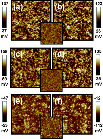 | ||
| Fig. 1 Surface potential mappings in the dark (a,c,e) and under illumination (b,d,f) on top of three kinds of interlayer structures. (a,b) Type I structure: ITO/P3HT:TiO2 NRs hybrid, (c,d) Type II structure: ITO/PEDOT:PSS/P3HT:TiO2 NRs hybrid, and (e,f) Type III structure: ITO/PEDOT:PSS/P3HT:TiO2 NRs hybrid/TiO2 NRs. The insets are topographic images of three kinds of interlayer structures. The image sizes are 5 × 5 μm. | ||
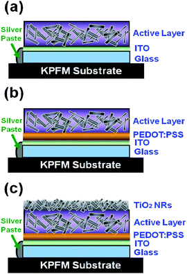 | ||
| Fig. 2 Schematic diagrams of three kinds of interlayer structures. (a) Type I structure: ITO/P3HT:TiO2 NRs, (b) Type II structure: ITO/PEDOT:PSS/P3HT:TiO2 NRs, and (c) Type III structure: ITO/PEDOT:PSS/P3HT:TiO2 NRs/TiO2 NRs. | ||
For a more detailed characterization of the charge behavior, we looked at changes in surface potential over time. Both negative shifts under illumination and recovery rates after switching off the light source for all three interlayer structures are plotted and shown in Fig. 3. Type II structure shows a slower recovery rate in surface potential as compared with that of Type I structure when the light was turned off after the illumination. It is because electrons and holes in Type I structure can be transported out immediately via ITO, but the PEDOT:PSS in Type II structure traps electrons in the active layer. A large negative shift under illumination was found in Type III structure due to an efficient electron transport by the TiO2 top layer. A large shift can also be inferred from the built-in electric field between the TiO2 hole blocking layer and PEDOT:PSS hole transporting layer. The photo-induced charges are thus collected more efficiently in Type III structure.
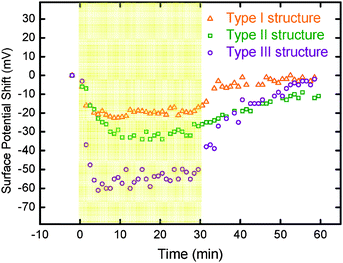 | ||
| Fig. 3 Plots of surface potential versus time for different interlayer structures of thin films. Type I structure (ITO/P3HT:TiO2 NRs), Type II structure (ITO/PEDOT:PSS/P3HT:TiO2 NRs), and Type III structure (ITO/PEDOT:PSS/P3HT:TiO2 NRs/TiO2 NRs). The yellow portion was measured for the first 30 min under halogen light illumination. | ||
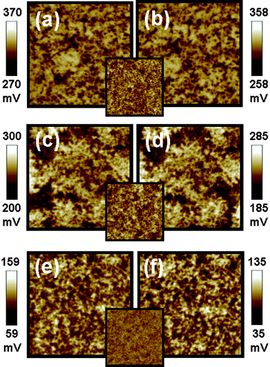
The performance of P3HT/TiO2 photovoltaic devices may vary with the molecular weight (MW) of P3HT, the solvent used in the processing and the type of ligand on the TiO2 NRs. KPFM was used to understand the correlation between surface potential of the active layer and device performance for these three parameters. We adopted Type II structure for this study, because it probes directly the surface potential changes of the P3HT/TiO2 active layer in our photovoltaic devices. The surface potential mapping images of P3HT/TiO2 NRs films fabricated from different P3HT molecular weights are shown in Fig. 4(a), (c), and (e) (in the dark) and Fig. 4(b), (d), and (f) (under illumination). The high MW P3HT sample shows a low surface potential (+142 mV) as compared to the medium MW sample (+392 mV) and the low MW sample (+310 mV) because the extent of well-connected networks and the degree of crystallinity of the high MW sample is higher than that of the others13 (Table 2). A high MW sample allows easier nanoscale phase separation and results in a better-connected percolated network which improves the device performance. A negative shift in the surface potential increases with increasing molecular weights; that is, −8 meV, −13 meV, and −28 meV for low, medium and high MW samples respectively. Moreover, we have measured the hole mobility of P3HT/TiO2 NRs film with different molecular weights of P3HT.13 The hole mobility for the low MW sample is about μh = 7.6 × 10⁻⁴ cm2 V−1 s−1 at E = 3.0 × 10⁴ V cm−1. For the medium MW sample, the hole transient exhibits dispersive character when the mobility increased to μh = 1.8 × 10⁻³ cm2 V−1 s−1 at E = 3.3 × 10⁴ V cm−1. For the high MW sample, the hole transient photocurrent becomes less dispersive with a clearly defined plateau region. The mobility for the high MW sample is further increased up to μh = 5.0 × 10⁻³ cm2 V−1 s−1 at E = 5.3 × 10⁴ V cm−1. These results indicate that hole mobility also increases with increasing the molecular weight of P3HT. In the case of high MW P3HT, enhanced π-electron delocalization enlarges the effective conjugation length. The electron mobility of the TiO2 NRs is not affected by the molecular weight of P3HT in the hybrid, because the weight ratio of TiO2 to P3HT with different MW is still 53:47. Thus, the reduction of surface potential is due to an increase in hole mobility.
 | ||
| Fig. 4 Surface potential mappings in the dark (a,c,e) and under illumination (b,d,f) of P3HT:TiO2 films made with low MW P3HT (a,b), medium MW P3HT (c,d) and high MW P3HT (e,f) on PEDOT:PSS/ITO substrate respectively. The insets are topographic images for P3HT:TiO2 films made with different molecular weight of P3HT. These image sizes are 5 × 5 μm. | ||
The solvents used in the fabrication of P3HT/TiO2 thin films can influence the performance of P3HT/TiO2 photovoltaic devices because of their influence on morphologies, absorption properties and carrier mobility of the P3HT/TiO2 active layers. We used KFPM to study the surface potential of P3HT/TiO2 thin films prepared from different solvents in the dark and under illumination. The results are shown in Fig. 5, and the insets are their AFM morphological images. The P3HT/TiO2 film spin coated from chloroform (CF) shows a rough topography, coarse surface potential distribution, and slight negative shift of surface potential, −12 mV. In the case of the trichlorobenzene (TCB) spin coated hybrid film, apparent phase separations are observed. The apparent phase separation causes the holes and electrons to trap in the P3HT and TiO2, so a smaller negative shift was observed (−15 mV). The hybrid film spin coated from chlorobenzene (CB) displays a smooth surface morphology and inter-connected percolated networks, so it has a more robust negative shift in surface potential (−24 mV). This result suggests that films fabricated from a good solvent such as CB, can help the formation of a more ordered structure of P3HT to facilitate good hole mobility, increasing the electron accumulation on the surface; consequently increasing the efficiency of charge separation and charge transport. For the hybrid film made with CF, the entangled P3HT would both decrease the contact area between donors and acceptors and reduce the charge separation. The poor charge transport can be predicted from the combination of isolated domains and entangled structures of the film made with CF. The surface potential properties and performances of the devices made with CF, TCB, and CB are summarized in Table 3. The highest short circuit current (2.73 mA) is observed in the CB-made device compared with the CF-made device (1.69 mA) and TCB-made device (2.52 mA). This result is consistent with the studies of surface potential and surface morphologies discussed before.
 | ||
| Fig. 5 Surface potential mappings in the dark (a,c,e) and under illumination (b,d,f) of P3HT:TiO2 films made with different solvents on PEDOT:PSS/ITO substrate. (a,b) The film made with chloroform, (c,d) the film made with trichlorobenzene, (e,f) the film made with chlorobenzene respectively. The insets are topographic images for P3HT:TiO2 films fabricated from different solvents. These image sizes are 5 × 5 μm. | ||
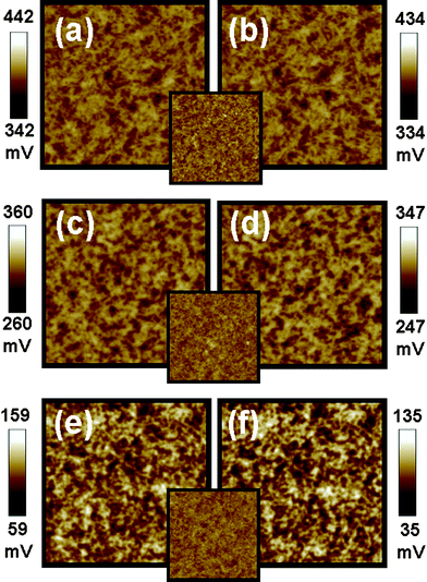
Due to an incompatibility between P3HT and TiO2 NRs, it is imperative to modify the surface of TiO2 NRs to have a homogeneous hybrid system. TiO2 NRs are usually synthesized in insulating oleic acid (OA). By replacing OA on the TiO2 NRs with a more conductive ligand, we have enhanced the device performance. For the ligand effect on the film morphology and the phase separation, the P3HT/TiO2 NRs film made from TiO2-OA is rough in topography with root-mean-square (RMS) roughness of 15.1 nm. For the film made from the TiO2-PYR and the TiO2-oligomer 3HT-COOH, a smooth film is obtained with uniformly distributed P3HTs and TiO2 NRs. The RMS roughness of the TiO2-PYR sample and the TiO2-oligomer 3HT-COOH sample are 4.5 nm and 3.6 nm, respectively. The uniform networks in these two films are believed to help the charge transport in the film. KPFM was used to study the surface potential of P3HT/TiO2 thin film prepared from TiO2 modified with different ligands. The results are shown in Fig. 6, and the inset are their AFM morphological images. Table 4 shows that when under illumination, the surface potential of the films are negatively shifted by −16 mV, −28 mV, and −42 mV for the films made from TiO2-oleic acid (TiO2-OA), TiO2-pyridine (TiO2-PYR), and TiO2-oligomer 3HT-COOH (TiO2-COOH), respectively. The lowest shift (−16 mV) is in the P3HT/TiO2-OA film because the non-conducting characteristic of oleic acid reduces charge separation and charge transport while increasing charge recombination. The moderately conductive ligand, pyridine, improves its separation and transport of charge carriers over that of the OA. Thus, a larger negative shift in the surface potential of the film is observed. Consequently, a better charge separation is expected for the P3HT/TiO2-PYR device as compared with the P3HT/TiO2-OA device (Table 4). The coordinated bonding between TiO2 NRs and pyridine is too weak to be an effective surface modifier for P3HT so, we replaced pyridine with the oligomer 3HT-COOH ligand. The carboxylic group of oligomer 3HT-COOH bonds strongly with the TiO2 which improves the surface coverage of oligomer 3HT-COOH on TiO2 NRs. In addition to the chemical bonding, the oligomer 3HT-end of oligomer 3HT-COOH also helps the smooth dispersion of the TiO2 NRs in the hybrid with a proper morphology for efficient charge separation. Furthermore, the overall dipole is generated from the oligomer 3HT to the carboxylic group, which assists electron transport through oligomer 3HT-COOH to TiO2. This accounts for the largest surface potential shift of oligomer 3HT-COOH ligand. Table 4 shows that the device fabricated from the material made from high MW P3HT and TiO2 NRs modified by oligomer 3HT-COOH exhibits the best device performance with a short circuit current of 3.26 mA cm−2 and a power conversion efficiency of 1.05%. When compared with pyridine, the oligomer 3HT-COOH contains delocalized π-electrons which facilitates better charge transport. Finally, the relatively large size of the oligomer 3HT-COOH reduces the charge recombination effectively due to its steric effect.17
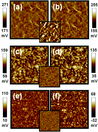 | ||
| Fig. 6 Surface potential mappings in the dark (a,c,e) and under illumination (b,d,f) of the P3HT:TiO2 film made with different TiO2 on PEDOT:PSS/ITO substrate, (a,b) the film made of TiO2 NRs with oleic acid ligand, (c,d) the film made of TiO2 NRs with pyridine ligand, (e,f) the film made with oligomer 3HT-COOH respectively. The insets are topographic images of P3HT:TiO2 films made from different TiO2. These image sizes are 5 × 5 μm. | ||
We have summarized the above data and replotted them in Fig. 7 which shows an excellent correlation between surface potential properties and device performance. It is interesting to note that changing the ligand on the TiO2 NRs had the largest effect on the power efficiency of the device. These results indicate that the function of ligands not only assist the separation and transportation of charge carriers but, also reduce the recombination of charge carriers very effectively. Our measurement of the surface potential of P3HT/TiO2 NRs bulk heterojunction device serves as a good guide for determining the performance of photovoltaic devices. Therefore, further research aimed at discovering new effective ligands for polymer-nanoparticle solar cell is an important direction for improving device performance.
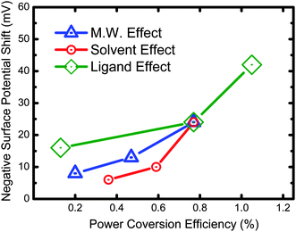 | ||
| Fig. 7 Correlation between surface potential properties and photovoltaic device performance of P3HT/TiO2. | ||
Conclusions
The surface potential mappings of P3HT/TiO2 NRs bulk heterojunction films by Kelvin probe force microscope have been used to study the surface charge accumulation by varying interlayer structures, processing solvents, P3HT molecular weights and ligands on TiO2 NRs. The addition of electron blocking layer and/or the hole blocking layer on the P3HT/TiO2 NRs film can facilitate the charge carrier transport and result in high surface potential shift. There is a clear correlation between surface charge potential of P3HT/TiO2 NRs films and their power conversion efficiency. Changing the ligand leads to the largest change in surface potential which has the greatest effect on the power conversion efficiency. Just changing the processing solvent is less effective and changing the molecular weight of P3HT is the least effective when compared with the changes of the ligands. The results of this study can serve as a useful guide for the fabrication of high performance heterojunction photovoltaic devices.Acknowledgements
Financial support obtained from the National Science Council of Taiwan (Project No. NSC95-3114-P-002-003-MY3 and NSC96-2628-E-002-017-MY3) is highly appreciated. The authors also thank Prof. Yang-Fang Chen of National Taiwan University, Dr Cheng-Si Tsao and Dr Chih-Min Chuang of Institute of Nuclear Energy Research for helpful discussions, Mr. Yu-Ching Huang, Mr Yu-Chia Liao and Mr Hsueh-Chung Liao of National Taiwan University for materials preparation and solar cells fabrication, and Mr An-Jey Su of Duquesne University (Pittsburgh, USA) for editing the manuscript.References
- G. Yu, J. Gao, J. Hummelen, F. Wudl and A. J. Heeger, Science, 1995, 270, 1789 CrossRef CAS.
- W. U. Huynh, J. J. Dittmer and A. P. Alivisatos, Science, 2002, 295, 2425 CrossRef CAS.
- M. D. McGehee, Materials Research Society Bulletin, 2009, 34, 95–100 CAS.
- H. Hoppe and N. S. Sariciftci, J. Mater. Chem., 2006, 16, 45 RSC.
- N. S. Sariciftci, D. Braun, C. Zhang, V. I. Srdanov, A. J. Heeger, G. Stucky and F. Wudl, Appl. Phys. Lett., 1993, 62, 585 CrossRef CAS.
- G. Li, V. Shortriya, J. Huang, T. Moriarty, K. Emery and Y. Yang, Nat. Mater., 2005, 4, 864 CAS.
- M. D. Michael, D. B. Buchholz, A. W. Hains, R. P. H. Chang and T. J. Marks, Proc. Natl. Acad. Sci. U. S. A., 2008, 105, 2783 CrossRef CAS.
- F. Silvestri, M. D. Irwin, L. Beverina, A. Facchetti, G. A. Pagani and T. J. Marks, J. Am. Chem. Soc., 2008, 130, 17640 CrossRef CAS.
- T. W. Zeng, Y. Y. Lin, C. W. Chen, W. F. Su, C. H. Chen, S. C. Liou and H. Y. Huang, Nanotechnology, 2006, 17, 5387–5392 CrossRef CAS.
- S. H. Park, A. Roy, S. Beaupré, S. Cho, N. Coates, J. S. Moon, D. Moses, M. Leclerc, K. Lee and A. J. Heeger, Nat. Photonics, 2009, 3, 297 Search PubMed.
- H. Y. Chen, J. Hou, S. Zhang, Y. Liang, G. Yang, Y. Yang, L. Yu, Y. Wu and G. Li, Nat. Photonics, 2009, 3, 649 Search PubMed.
- P. Ravirajan, S. A. Haque, J. R. Durrant, D. D. C. Bradley and J. Nelson, Adv. Funct. Mater., 2005, 15, 609 CrossRef CAS.
- M. C. Wu, C. H. Chang, H. H. Lo, Y. S. Lin, C. W. Chen, W. C. Yen, Y. Y. Lin, Y. F. Chen and W. F. Su, J. Mater. Chem., 2008, 18, 4097 RSC.
- C. Y. Kwong, A. B. Djurii, P. C. Chui, K. W. Cheng and W. K. Chan, Chem. Phys. Lett., 2004, 384, 372 CrossRef CAS.
- C. Goh, S. R. Scully and M. D. McGehee, J. Appl. Phys., 2007, 101, 114503 CrossRef.
- R. H. Lohwasser, J. Bandara and M. Thelakkat, J. Mater. Chem., 2009, 19, 4126 RSC.
- Y. Y. Lin, T. H. Chu, S. S. Li, C. H. Chuang, C. H. Chang, W. F. Su, C. P. Chang, M. W. Chu and C. W. Chen, J. Am. Chem. Soc., 2009, 131, 3644 CrossRef CAS.
- Y. Y. Lin, T. H. Chu, C. W. Chen and W. F. Su, Appl. Phys. Lett., 2008, 92, 053312 CrossRef.
- J. Bouclé, S. Chyla, M. S. P. Shaffer, J. R. Durrant, D. D. C. Bradley and J. Nelson, Adv. Funct. Mater., 2008, 18, 622 CrossRef CAS.
- R. H. Friend, G. J. Denton, J. J. M. Halls, N. T. Harrison, A. B. Holmes, A. Kohler, A. Lux, S. C. Moratti, K. Pichler, N. Tessler, K. Towns and H. F. Wittmann, Solid State Commun., 1997, 102, 249 CrossRef CAS.
- T. J. Savenije, J. M. Warman and A. Goossens, Chem. Phys. Lett., 1998, 287, 148 CrossRef CAS.
- A. C. Arango, L. R. Johnson, V. N. Bliznyuk, Z. Schlesinger, S. A. Carter and H. H. Horhold, Adv. Mater., 2000, 12, 1689 CrossRef CAS.
- V. Palermo, M. Palma and P. Samorì, Adv. Mater., 2006, 18, 145 CrossRef CAS.
- A. Liscio, G. D. Luca, F. Nolde, V. Palermo, K. Müllen and P. Samorì, J. Am. Chem. Soc., 2008, 130, 780 CrossRef CAS.
- T. Glatzel, D. Fuertes Marrón, Th. Schedel-Niedrig, S. Sadewasser and M. Ch, Appl. Phys. Lett., 2002, 81, 2017 CrossRef CAS.
- H. Hoppe, T. Glatzel, M. Niggemann, A. Hinsch, M. Ch. Lux-Steiner and N. S. Sariciftci, Nano Lett., 2005, 5, 269 CrossRef CAS.
- V. Palermo, M. Palma and P. Samorì, Adv. Mater., 2006, 18, 145–164 CrossRef CAS.
- V. Palermo, G. Ridolfi, A. M. Talarico, L. Favaretto, G. Barbarella, N. Camaioni and P. Samorì, Adv. Funct. Mater., 2007, 17, 472 CrossRef CAS.
- A. Liscio, G. D. Luca, F. Nolde, V. Palermo, K. Müllen and P. Samorì, J. Am. Chem. Soc., 2008, 130, 780 CrossRef CAS.
- V. Palermo, M. B. J. Otten, A. Liscio, E. Schwartz, P. A. J. de Witte, M. A. Castriciano, M. M. Wienk, F. Nolde, G. De Luca, J. J. L. M. Cornelissen, R. A. J. Janssen, K. Müllen, A. E. Rowan, R. J. M. Nolte and P. Samorì, J. Am. Chem. Soc., 2008, 130, 14605 CrossRef CAS.
- T. Glatzel, M. Rusu, S. Sadewasser and M. Ch. Lux-Steiner, Nanotechnology, 2008, 19, 145705 CrossRef.
- S. Sadewasser, T. Glatzel, S. Schuler, S. Nishiwaki, R. Kaigawa and M. C. Lux-Steiner, Thin Solid Films, 2003, 431–432, 257 CrossRef CAS.
- M. Chiesa, L. Bürgi, J. S. Kim, R. Shikler, R. H. Friend and H. Sirringhaus, Nano Lett., 2005, 5, 559 CrossRef CAS.
- P. Matyba, K. Maturova, M. Kemerink, N. D. Robinson and L. Edman, Nat. Mater., 2009, 8, 672 CrossRef CAS.
- T. W. Zeng, F. C. Hsu, Y. C. Tu, T. H. Lin and W. F. Su, Chem. Phys. Lett., 2009, 479, 105 CrossRef CAS.
- C. A. Dai, W. C. Yen, Y. H. Lee, C. C. Ho and W. F. Su, J. Am. Chem. Soc., 2007, 129, 11036 CrossRef CAS.
- A. S. Amarasekara and M. Pomerantz, Synthesis, 2003, 2003, 2255.
Footnotes |
| † Electronic supplementary information (ESI) available: Additional information. See DOI: 10.1039/b9nr00385a |
| ‡ These authors contributed equally to this work. |
| This journal is © The Royal Society of Chemistry 2010 |