Bias-dependent photocurrent response in protein nanolayer-embedded solid state planar diode devices
Sungho
Nam
,
Hwajeong
Kim
* and
Youngkyoo
Kim
*
Organic Nanoelectronics Laboratory, Department of Chemical Engineering, Kyungpook National University, Daegu, 702-701, Republic of Korea. E-mail: ykimm@knu.ac.kr; khj217@knu.ac.kr; Fax: +82 53 950 6615; Tel: +82 53 950 5616 Web: http//one.knu.ac.kr
First published on 26th February 2010
Abstract
A bias-dependent superlinear photocurrent response under white light illumination was measured in the planar diodes with a protein nanolayer of horseradish peroxidase (HRP) that is a key material for sensing hydrogen peroxide in biological systems.
A growing interest in extending human life has triggered expansion of nanobiotechnology researches and markets for nanomedicines, biosensors, biomedical devices, etc.1 Most current device technologies for biomedical applications are limited to field-effect transistors (FET) and/or microfluidic devices which are based on electrochemical and/or microelectromechanical system (MEMS) infrastructures.2–5 However, in order to improve the performance of such devices as well as to realize low-cost manufacturing and wide-spreading, the invention of much smarter device architectures is of crucial importance for integrative biological systems.
For the design of brand-new device architectures, it is essential to understand the intrinsic electrical properties of biomaterials such as DNA, proteins, enzymes, etc.6,7 To date, a series of studies has been reported on the electrical properties of DNA molecules and/or oligonucleotides.7 However, the electrical properties of proteins were very rarely studied because proteins are bigger than DNA and have complex molecular structures, so they were understood as a class of insulating materials.
Of the various proteins, horseradish peroxidase (HRP), which possesses a metal-containing heme, has been studied in the field of biosensors, enzyme-linked immunosorbent assay (ELISA), and immunohistochemistry for a century or more.8–11 The reason is that it plays a core role in detecting hydrogen peroxide (H2O2) molecules due to the conversion reaction of H2O2 to H2O through an oxidation process by ferric heme.9,11,12 However, the electrical properties of HRP were not studied in a form of solid state nanolayer embedded (coated) in a diode structure even though a variety of studies has been carried out in solutions.
In this work, we attempted to fabricate a fully solid state planar diode device with the HRP nanolayer and tried to examine the electrical properties of the devices. In particular, the photovoltaic responses of devices have been measured to investigate the possibility of charge generation by photon energy, which can be applied for light-aided biomedical therapeutic applications.13
HRP (180 U mg−1, where 1 U = the amount of the enzyme which catalyzes the conversion of 1 μmol substrate per min) was purchased from Toyobo Co. Ltd and used without further purification. The HRP solutions were prepared using distilled water at a solid concentration of 30 mg ml−1. As shown in Fig. 1, a planar diode device structure was employed: patterned indium tin oxide (ITO) stripes were used as electrodes whose gap (channel length) was 60 μm (channel width = 3 mm). Prior to the device fabrication, the patterned ITO-glass substrates were cleaned ultrasonically using acetone and isopropyl alcohol, followed by drying with a nitrogen flow. The HRP nanolayer was formed by either spin-coating or drop-coating on top of the patterned ITO-glass substrates; the average thickness of HRP nanolayer was ∼100 nm alongside some thicker (∼700 nm) parts (see Fig. 1c). Then the coated samples were dried for 3–4 h in a vacuum oven to get rid of any remaining solvent molecules. The thickness of HRP nanolayers was measured using a surface profiler (Alpha-step 200, Tencor). The optical absorption spectra of HRP nanolayers and solutions were measured using UV-visible spectrophotometer (Optizen 2120, MECASYS), while the electrical characteristics of devices were measured using a semiconductor analyzer (Model 4200-SCS, Keithley). The surface morphology of HRP nanolayers was measured using atomic force microscope (AFM, Nanoscope IIIa, Digital Instrument, USA) and field emission–scanning electron microscope (FE-SEM, S-4300&EDX-350, Hitachi). The photoresponse characteristics of devices were measured under illumination of simulated solar light (air mass 1.5 G, 100 mW cm−2) using a solar simulator (Model 92250, Newport-Oriel).
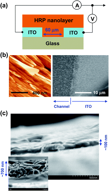 | ||
| Fig. 1 (a) Schematic illustration of cross-sectional device structure. (b) AFM images of HRP nanolayer (left) and FE-SEM images of HRP aggregates formed by drop-casting from a dilute solution (right). (c) FE-SEM images of HRP nanolayers formed by spin-coating. | ||
As shown in Fig. 2, the absorption spectrum of HRP nanolayer covers a broad range of the UV-visible region with three major peaks at around 405 nm (the Soret band), 514 nm, and 654 nm. This absorption spectrum is in good agreement with that of the HRP solution (in water), which indicates that the HRP nanolayer was coated without huge degradation (inset to Fig. 2). It is noteworthy that the optical absorption by heme is a useful probe for the study of conformation change in a variety of heme proteins. In this study, the broad UV-visible spectrum of HRP nanolayers motivated us to choose the white light (almost similar to solar spectrum) as an optical excitation tool (stimulator) for the examination of photocurrent generation.
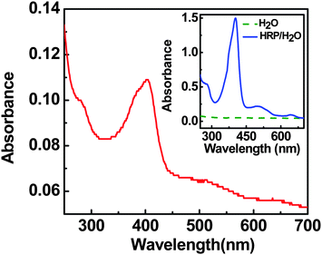 | ||
| Fig. 2 UV-visible absorption spectra of HRP nanolayer coated on quartz substrate and (inset) HRP solution in water. | ||
The current–voltage (I–V) characteristics of planar devices with the HRP nanolayer were measured in the dark and then under illumination of white light. As shown in Fig. 3, the dark I–V curves exhibited an almost linear behavior in both forward and reverse bias directions, indicating that the present planar device belongs to a class of ohmic devices in the given scale of applied voltages (−10 to +10 V). Under illumination of white light, however, the planar device showed higher current at the applied voltage of >2.5 V, compared to the current measured in the dark. This tells us that we have a photocurrent from the present planar device with the HRP nanolayer. Here we note that the slightly different current gap between dark and illumination in forward (positive voltages) and reverse (negative voltages) bias can be attributed to the marginally different morphological environment for charge injection and transport, because the interfacial contact between electrodes and HRP molecules on each electrode cannot be controlled to be exactly identical by wet-coating processes. It is particularly noteworthy that the light I–V curves exhibited a superlinear trend as a function of voltage, which is different from the dark I–V curves. This phenomenon is understood as the result of free charge carriers generated by photons absorbed in the HRP nanolayer. The fact that there was a higher current in the dark than in the light at voltages less than 2.5 V, and a reverse trend at voltages above 2.5 V, can be explained by the compensation of the net charge of HRP under illumination.14 In addition, this can be in part attributed to the reduced charging effect in the HRP nanolayer under illumination at lower voltages when it comes to the fact that the charging effect is more serious in insulating materials than conductive materials. In other words, the charged carriers under a higher applied electric field could be easily retrieved due to the improved conductivity (reduced resistivity) in the HRP nanolayer under illumination.
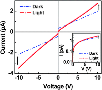 | ||
| Fig. 3 Current–voltage (I–V) characteristics of planar device coated with HRP nanolayer: Measurement was performed from 0 V to ±10 V under dark and white light illumination (100 mW cm−2). Inset shows the replotted I–V curves in semi-logarithmic scale. | ||
To investigate the nature of the photocurrent in the present planar device, we tried to turn on and off the incident light by varying the applied voltages. As shown in Fig. 4a, the device current responded clearly to the switching of incident light. Interestingly, a photocurrent was measured even at 0 V, indicative of photocurrent generation under the short circuit condition which is an important function for applications as energy devices in integrative biological systems. When the incident light was turned on, the device current did very quickly rise and then showed a (exponential) decay with a stabilization trend at 0 V. After turning off, the device current quickly disappeared at this voltage. At higher voltages (≥2.5 V), the device current showed similar quick rise upon turn-on of light but it exhibited an on-going increase under continuous increase in voltage. This increasing trend was more pronounced when the applied voltage was increased.
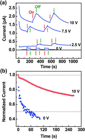 | ||
| Fig. 4 (a) Voltage-dependent photocurrent as a function of time upon turning the incident white light on and off (100 mW cm−2). (b) Comparison of photocurrent decay as a function of time at the voltage of 0 V and 10 V. | ||
After the light was turned off, the device current was decayed but the decay rate became much slower as the voltage was higher (Fig. 4b). We think that the voltage-dependent rising and decaying trend is related to the extraction rate of photogenerated charges because the heme part of HRP, which is the major active part for absorbing the photons leading to photocurrent generation after a charge separation process, is mostly shielded by surrounding groups that are considered to be electrically insulating. In other words, the penetration of photogenerated charges through the insulative shielding parts in HRP might be the rate-determining step in the present solid state HRP device.
In conclusion, we have fabricated a planar diode device with the HRP nanolayer as an active micro-channel that undergoes an integrative function including a photon absorption as well as charge generation and transport. The optical absorption spectrum of the HRP nanolayer was almost identical to that of HRP solution, indicating no degradation of HRP during wet processing. Considering the dark I–V characteristics, the present device was assigned to the ohmic device category. Under illumination, however, the device current became superlinear, indicative of transition toward a diode-like device. The current gap between the dark and illumination at lower voltages was assigned to either the net charge compensation or the field-induced charging effect, which is closely related to the ohmic nature of the present device. The present device did clearly respond to the switching of incident light, confirming that the device current was indeed a photocurrent. The voltage (bias)-dependent rising and decaying trend was considered to be related to the extraction rate of photogenerated charges from the photoactive heme position.
Acknowledgements
This work was financially supported by Korean government grants (Priority Research Center Program: 2009-0093819, Pioneer Research Center Program: 2009-0082820, NRF: 20090072777).Notes and references
- Fractal analysis of the binding and dissociation kinetics for different analysis on biosensor surfaces, ed. A. Sadana and N. Sadana, Elsevier, Amsterdam, 2007 Search PubMed.
- N. Mohanty and V. Berry, Nano Lett., 2008, 8, 4469 CrossRef CAS.
- Bioelectronics, ed. I. Willner and E. Katz, Wiley-VCH Verlag GmbH & Co. KGaA, Weinheim, 2005 Search PubMed.
- D. Juncker, H. Schmiz and E. Delamarche, Nat. Mater., 2005, 4, 622 CrossRef CAS.
- A. C. R. Grayson, R. S. Shawgo, A. M. Johnson, N. T. Flynn, Y. Li, M. J. Cima and R. Langer, Proc. IEEE, 2004, 92, 6 CrossRef CAS.
- H. Kim, P. Degenaar and Y. Kim, J. Phys. Chem. C, 2009, 113, 14377 CrossRef CAS.
- C. Nogues, S. R. Cohen, S. S. Daube and R. Naaman, Phys. Chem. Chem. Phys., 2004, 6, 4459 RSC.
- A. C. Patel, S. Li, J. Yuan and Y. Wei, Nano Lett., 2006, 6, 1042 CrossRef CAS.
- B. X. Gu, C. X. Xu, G. P. Zhu, S. Q. Liu, L. Y. Chen, M. L. Wang and J. J. Zhu, J. Phys. Chem. B, 2009, 113, 6553 CrossRef CAS.
- N. C. Veitch, Phytochemistry, 2004, 65, 249 CrossRef CAS.
- Biosensors and modern biospecific analytical techniques, ed. L. Gorton, Elsevier, Amsterdam, 2005 Search PubMed.
- G. I. Berglund, G. H. Carlsson, A. T. Smith, H. Szoke, A. Henriksen and J. Hajdu, Nature, 2002, 417, 463 CrossRef CAS.
- Medical devices and systems, ed. J. D. Bronzino, CRC Press, Florida, 2006 Search PubMed.
- S. Nam, H. Kim and Y. Kim, 2009, in preparation.
| This journal is © The Royal Society of Chemistry 2010 |