Surface plasmon resonance in interacting Si nanoparticle chains
Juan
Wang
ac,
Xiao-Jing
Wang
a,
Yang
Jiao
a,
Ming-Wen
Chu
b,
Marek
Malac
c and
Quan
Li
*a
aDepartment of Physics, the Chinese University of Hong Kong, Shatin, New Territory, Hong Kong. E-mail: liquan@phy.cuhk.edu.hk
bCenter for Condensed Matter Sciences, National Taiwan University, Taipei, 106, Taiwan
cNational Institute for Nanotechnology, 11421 Saskatachewan Drive, Edmonton Alberta, Canada T6G 2M9
First published on 16th February 2010
Abstract
Interaction between the adjacent nanoparticles in a one-dimensional Si nanoparticle chain results in splitting of the surface plasmon resonance (SPR) into transverse and longitudinal polarizations, as well as spatial re-distribution of the SPR intensity, leading to local field enhancement in between the two nanoparticles. Such interaction is directly visualized using electron energy loss spectroscopy related techniques, which also disclose the longer impact parameter associated with the longitudinal mode SPR (as compared to that of the transverse mode SPR). By controlling the growth of Si nanostructures into different morphologies, we demonstrate that the material's optical properties can be manipulated.
Introduction
Surface plasmon resonance (SPR) in interacting nanoparticle assemblies has recently attracted much research attention due to their capability to transport and guide the electromagnetic energy below the diffraction limit of light in nano-optics.1,2 Most of the literature work have been carried out in noble metal nanoparticle ensembles and interacting plasmon mode has been demonstrated for particle separation distances in the range of tens of nanometres, i.e. one order of magnitude lower than the excitation light wavelength.3–5 Surface plasmon in interacting systems made of other materials (e.g. Si) has rarely been investigated, although they could also be of technological interest for ultraviolet (UV) photonic applications due to their much higher SPR energies, as compared to those of noble metals in the IR region.Although near-field optical microscopy has been widely used to study the surface plasmon in interacting nanoparticle systems, the best spatial resolution achieved is in the sub-wavelength range, i.e. ∼50 nm.6,7 Consequently, for nanoparticles of smaller size and/or particle ensembles of shorter separation distance, mapping of the local plasmonic properties remains difficult. On the other hand, transmission electron microscopy-electron energy loss spectroscopy (TEM-EELS) has been recently employed as an alternative technique to study the SPR of individual nanoparticles and their ensembles.8,9 The excellent spatial resolution of the technique enables the mapping of local variations in the material's dielectric response at the nanometre scale. Although caution has to be taken, qualitative agreement between the EELS results and the material's photonic response make it a powerful tool in probing the local plasmonic properties of nano-objects.10–13
In the present study, we have investigated the SPR in Si nanoparticle chains, in which the Si nanoparticles are ∼12 nm in diameter, and they are assembled into one-dimensional chain-like structures by embedding in SiO2. The separation distance between individual particles is in the range of several to several tens of nanometres. Different surface plasmon modes, in particular their spatial distribution and possible interactions, are directly visualized using electron energy loss spectroscopy (EELS), and the impact of interaction is discussed. The interaction among specific plasmon modes leads to distinct absorption properties of the nanoparticle chains, which is also observed on the macroscopic scale.
Experimental
The Si nanoparticle chains were synthesized via thermal evaporation of SiO powder in a high temperature vacuum tube furnace.14 Pure Ar gas was introduced as the carrier gas, and the total pressure of the system was kept at 200 mbar for the whole fabrication process. The source material was heated up to 1300 °C for 2 h before the tube furnace was eventually cooled down to room temperature, and the products were collected at the temperature zone of ∼1000 °C in the downstream of the tube furnace. A higher processing pressure of ∼300 mbar leads to the formation of other forms of Si nanostructures, i.e. Si nanowires (being collected at the 900–1000 °C temperature zone), and well separated Si nanoparticles (being collected at the 1100 °C temperature zone).15 The products were annealed at 700 °C in an oxygen atmosphere for 20 min before being taken out from the tube furnace. The morphology and microstructure of the products were characterized using a transmission electron microscope (TEM, Tecnai G2) with a Gatan Imaging Filter (GIF, Tridiem™) attached to it. Spatially resolved electron energy loss spectra were acquired in the scanning transmission electron microscopy (STEM) line scan mode with the electron probe size of ∼0.5 nm and energy resolution of ∼0.5 eV. The energy filtered TEM (EFTEM) images were taken using a 2 eV slit centered at specific energy positions of interest. The optical extinction spectra of all the products (dispersed in ethanol) are measured using a UV-vis spectrometer (Hitachi spectrophotometer U-3501).Results and discussions
We start our discussion with an isolated Si nanoparticle. Fig. 1a shows the EFTEM image (using a 2 eV slit centered at the Si bulk plasmon resonance ∼16.9 eV) of a spheroid nanoparticle with ∼12 nm diameter, embedded in the wire-like SiO2 matrix. A slight elongation of the spheroid is observed along the wire's axial direction, and the surface oxide thickness is ∼3 nm. An EELS line scan has been taken across the nanoparticle along the wire's axial direction (as marked by the red line in Fig. 1a). Si bulk plasmon at ∼16.9 eV dominates the EEL spectra (Fig. 1b) with a weak peak appearing at ∼7.8 eV when the electron probe is located on the nanoparticle. The intensity of the Si bulk plasmon peak drastically decreases when the electron probe moves away from the particle and spectrum features characteristic of SiO2 become obvious. At the same time, a slight red shift of the ∼7.8 eV peak occurs.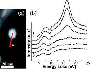 | ||
| Fig. 1 (a) Energy filtered TEM (EFTEM) image of an isolated Si particle embedded in a SiO2 nanowire; (b) the corresponding EELS line scan spectra starting from the particle center to the SiO2 matrix wire along the chain axial direction. | ||
The ∼7.8 eV peak is commonly understood as the surface plasmon arising from the Si surface surrounded by SiO2 medium. In spherical particles with diameters below 100 nm, the oscillation frequency of the surface plasmon can be generally estimated using point dipole approximation. Although the SPR energy is expected to change with the size of the particles, such an effect is rather weak for particle diameter <100 nm.16 The shape deviation from a perfect spheroid to ellipsoid could have a more profound effect, i.e. a splitting in the SPR energy would occur, with one appearing at higher energy, and the other at lower energy, corresponding respectively to the transverse and longitudinal polarization of the surface plasmon.17 However, the energy difference between the two split peaks would also be fairly small for a slightly elongated spheroid18—such as the one shown in Fig. 1. Consequently, it would be difficult to identify two distinct peaks (transverse and longitudinal modes) in the EEL spectra (as limited by the energy resolution and the signal to noise ratio of the technique) taken on such Si nanoparticles, but a “red-shift” of the SPR when the electron probe moves aloof the nanoparticle along the chain axial direction can be observed.19
The electron probe then scans across multiple nanoparticles with an inter-particle separation of ∼30 nm, which is shown in Fig. 2a (the inter-particle separation is defined as from edge to edge). The diameter of the Si nanoparticles in the chain and its surface oxide thickness are similar to those of the isolated Si nanoparticle in Fig. 1a. The SPR peak is observed to red shift from ∼7.8 eV to ∼6.7 eV when the electron probe moves from the center of the Si nanoparticle to the SiO2 connection wire, with the SPR intensity significantly weakened in the middle of the two particles. This red shift is only slightly larger than that in isolated particles. However, a distinct difference in the EEL spectra is observed when inter-particle separation reduces to ∼20 nm in Fig. 2c. When the electron probe is located on the Si nanoparticle, the SPR appears at ∼8 eV, but with a plateau-like shoulder intensity extending to ∼5.5 eV. As the e-probe scans away from the nanoparticle, a decrease in the ∼8 eV peak intensity is observed simultaneously with an increase in the ∼5.5 eV one (Fig. 2d). A similar trend is observed in the particle chain with shorter inter-particle spacing (i.e. ∼10 nm in Fig. 2e), but with one peak occurring at slightly higher energy, i.e. ∼ 8.1 eV (as compared to 8 eV), and the other at even lower energy, i.e. 4.8 eV (as compared to 5.5 eV), in Fig. 2f. In the extreme case, i.e. the Si nanoparticles are about to touch/touching each other in the chain, forming a continuous wire-like morphology (Fig. 2g), little variation is observed in the EEL spectra as the e-probe scans to different positions on the chain. A low energy peak at ∼4.2 eV is constantly observed in all of the spectra, while another weak feature can be barely discerned at ∼8.2 eV.
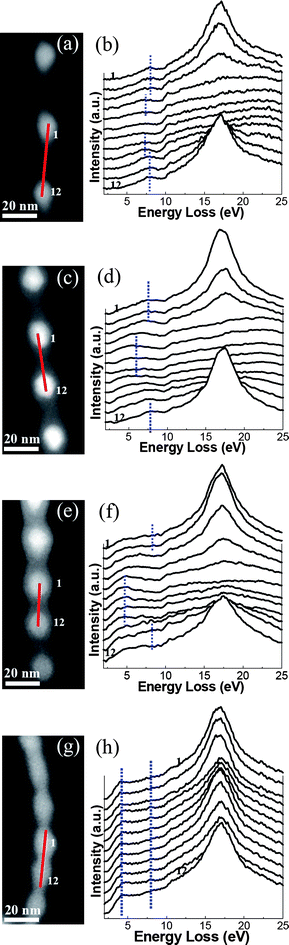 | ||
| Fig. 2 EFTEM images of four particle chains with different inter-particle spacings, i.e. (a) ∼30 nm, (c) ∼20 nm, (e) ∼10 nm and (g) ∼0 nm; (b), (d), (f) and (h) the corresponding EELS line scan spectra taken across the Si particles along the chain axial direction. | ||
Fig. 3 plots the experimental SPR data as a function of the inter-particle separation, with the error bar being determined by the energy resolution of EELS, i.e. 0.5 eV. Intuitively, when the nanoparticles are far apart from each other, they can be treated as isolated particles. On the other hand, when the nanoparticles in the chain are getting closer and closer, eventually a continuous thin nanowire would be formed. The single SPR in isolated spherical nanoparticle (at ∼7.8 eV) is found to split into two branches when individual particles are assembled to form a one-dimensional particle chain, with one appearing at higher energies and the other at low energies. When the inter-particle separation gets shorter and shorter, a blue shift and a red shift have been observed respectively in the high and low energy SPR branches, until ∼8.2 eV, and ∼4.2 eV are reached in the case of thin nanowire, corresponding respectively to the multipole and monopole modes of the SPR in the nanowire.15
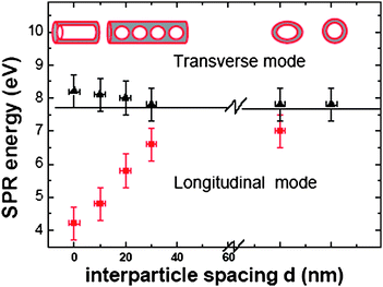 | ||
| Fig. 3 The SPR energy as a function of the inter-particle separation, measured from the experimental EEL spectra of different particle chains and isolated particles. | ||
The observed splitting for SPR is a piece of direct evidence of the dipolar interactions between adjacent particles.3 In such a model, the nanoparticles in the chain can be treated as an assembly of interacting dipoles, and the interactions between the particles can align the dipole fields, forming collective dipole oscillations in the particle chain. When the nanoparticles are getting closer to each other, a continuous change in the charge distributions on the particle chain would occur as mediated by the interaction of dipole fields on neighboring particles.20–22 The Coulomb force interactions between the electrons in neighboring particles would then cause a blueshift for polarization perpendicular to the chain axis (the high energy branch in the split SPR, corresponding to the transverse SPR mode), and a red-shift for the longitudinal polarization (the low energy branch in the split SPR).23 This is consistent with our experimental observations summarized in Fig. 3.
The interactions between the particles can be directly visualized in the energy filtered TEM (EFTEM) images of the Si nanoparticle chains taken at specific energy losses. Fig. 4 compares the EFTEM images of two different Si nanoparticle chains (with inter-particle separation of (a) ∼30 nm, and (b) ∼10 nm, respectively) taken at 0 eV (corresponding to bright filed TEM image), 17 eV (Si bulk plasmon resonance), 8 eV (transverse mode SPR), and 5 eV (longitudinal mode SPR). To obtain a more straight-forward comparison of different plasmon mode intensity vs. their spatial distribution, the intensity profiles of the 17 eV, 8 eV, and 5 eV maps are retracted along the longitudinal direction of the nanoparticle chain (as marked by the rectangular boxes in the corresponding maps), and are plotted in Fig. 4c and d. One can see that for both particle chains alike, the Si bulk plasmon is highly localized on the Si nanoparticles, while the 8 eV SPR is mainly confined to the spherical interface between the Si nanoparticle and SiO2 surface layer. As a comparison, the spatial distribution of the 5 eV SPR is very different—although it is still located on the spherical interface between Si and SiO2, a stronger intensity is found on both edges of the Si particles along the chain axial direction. When the nanoparticles are very close together (∼5 nm interparticle separation, as marked by the arrow in Fig. 4d), the strongest intensity moves to in between two adjacent nanoparticles, rather than being located on the Si particle surface, confirming the greatly enhanced field between the particles—another indication of the coupling. One of the major differences between the ∼8 eV (transverse polarization) and the ∼5 eV (longitudinal polarization) is their electron impact parameter, with the latter being much longer than the former along the axial direction of the particle chain.24 Consequently, the dipolar interactions between the nanoparticles would exert a stronger effect on the longitudinal mode SPR (including the obvious red-shift in the SPR energy and its intensity spatial re-distribution), but a weaker effect on the transverse mode of SPR (small blue shift in the SPR energy).
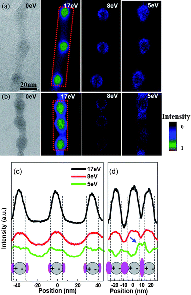 | ||
| Fig. 4 (a) and (b) EFTEM images of two particle chains with different inter-particle spacing: ∼30 nm and ∼10 nm, imaged at energy losses of 0 eV, 17 eV, 8 eV and 5 eV using a 2 eV width slit; (c) and (d) the intensity profiles retracted along the longitudinal directions of the two Si nanoparticle chains. | ||
The interaction between the nanoparticles in the chain would result in a distinct characteristic in their absorption properties. By controlling the fabrication of Si nanostructure samples into three different morphologies, i.e. well separated Si nanoparticles connected by SiO2 nanowires, periodically distributed Si nanoparticles in the SiO2 nanowire (i.e. the nanoparticle chains with inter-particle separation of 20 ± 15 nm), and Si/SiO2 core-shell nanocables, one can manipulate the optical property of such materials. Fig. 5 shows the optical extinction spectra and corresponding bright field (BF) TEM images of these three products. While there is no distinct feature presented in the extinction spectrum of the well separated Si particles (sample a), a broad extinction band centered at ∼5 eV is observed above the 3.4 eV excitation threshold of Si for the nanoparticle chains (sample b). A similar extinction band has also been revealed in the Si/SiO2 core-shell nanocables (sample c), but at a lower energy of ∼4.2 eV.
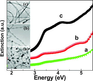 | ||
| Fig. 5 The low magnification TEM images and the optical extinction spectra of (a) well separated Si nanoparticles (connected by SiO2 nanowire), (b) nanoparticle chains with inter-particle separation of 20 ± 15 nm, and (c) Si/SiO2 core-shell nanocables. | ||
One shall note that the absorption measurement was performed on the macroscopic scale, so that the broadened extinction spectrum would represent the average behavior of the nanoparticle chains with different inter-particle separations (ranging from 5 to 35 nm). In addition, the SPR modes in individual Si nanostructures are essentially broader than those in metals, as the imaginary part of the dielectric function of Si is large. This suggests that Si may be less competitive to metals, such as Au, in the applications of waveguides and sensors.
Conclusions
In conclusion, the surface plasmon resonance in closely packed one-dimensional Si nanoparticle assemblies has been directly visualized using EELS and EFTEM imaging, which are techniques that enjoy spatial resolutions down to the nanometre scale. Near-field interactions between the adjacent nanoparticles result in splitting of the surface plasmon resonance into transverse and longitudinal polarizations with different spatial distributions. In particular, spatial re-distribution and enhancement of the longitudinal mode SPR intensity are observed to occur when the inter-particle separation is shorter than 10 nm. The experimental observation suggests possible tuning of the surface plasmons and local electromagnetic field enhancement by adjusting the interparticle separation in the one-dimensional particle chain, which may find promising applications in functional UV optical devices below the diffraction limit of light.Acknowledgements
This work is supported by the grants for the SEG large equipment (CUHK_06) and the CUHK Focused Investment Scheme C. Additional support was obtained from the National Institute for Nanotechnology (NINT) and Natural Sciences and Engineering Research Council (NSERC), Canada.Notes and references
- S. A. Maier, P. G. Kik, H. A. Atwater, S. Meltzer, E. Harel, B. E. Koel and A. A. G. Requicha, Nat. Mater., 2003, 2, 229 CrossRef CAS.
- M. Quinten, A. Leitner, J. R. Krenn and F. R. Aussenegg, Opt. Lett., 1998, 23, 1331 Search PubMed.
- J. R. Krenn, A. Dereux, J. C. Weeber, E. Bourillot, Y. Lacroute, J. P. Goudonnet, G. Schider, W. Gotschy, A. Leitner, F. R. Aussenegg and C. Girard, Phys. Rev. Lett., 1999, 82, 2590 CrossRef CAS.
- S. A. Maier, P. G. Kik and H. A. Atwater, Appl. Phys. Lett., 2002, 81, 1714 CrossRef CAS.
- M. L. Brongersma, J. W. Hartman and H. A. Atwater, Phys. Rev. B: Condens. Matter Mater. Phys., 2000, 62, R16356 CrossRef CAS.
- K. Lieberman, N. Ben-Ami and A. Lewis, Rev. Sci. Instrum., 1996, 67, 3567 CrossRef.
- T. Klar, M. Perner, S. Grosse, G. von Plessen, W. Spirkl and J. Feldman, Phys. Rev. Lett., 1998, 80, 4249 CrossRef CAS.
- J. Nelayah, M. Kociak, O. Stéphan, F. J. García de Abajo, M. Tencé, L. Henrard, D. Taverna, I. Pastoriza-Santos, L. M. Liz-Marzán and C. Colliex, Nat. Phys., 2007, 3, 348 CrossRef CAS.
- B. Schaffer, U. Hohenester, A. Trügler and F. Hofer, Phys. Rev. B: Condens. Matter Mater. Phys., 2009, 79, 041401 CrossRef.
- U. Hohenester, H. Ditlbacher and J. R. Krenn, Phys. Rev. Lett., 2009, 103, 106801 CrossRef.
- J. Nelayah, L. Gu, W. Sigle, C. T. Koch, I. Pastoriza-Santos, L. M. Liz-Martin and P. A. van Anken, Opt. Lett., 2009, 34, 1003 Search PubMed.
- A. Rivacoba, N. Zabala and J. Aizpurua, Prog. Surf. Sci., 2000, 65, 1 CrossRef CAS.
- M. W. Chu, V. Myroshnychenko, C. H. Chen, J. P. Deng, C. Y. Mou and F. J. García de Abajo, Nano Lett., 2009, 9, 399 CrossRef CAS.
- Q. Li and Y. Jiao, Appl. Phys. Lett., 2005, 87, 261905 CrossRef.
- J. Wang, X. J. Wang, Y. Jiao, Q. Li, M. W. Chu and M. Malac, Appl. Phys. Lett., 2009, 95, 133102 CrossRef.
- G. Mie, Ann. Phys., 1908, 330, 377 CrossRef.
- Y. Xia and N. J. Halas, MRS Bull., 2005, 30, 338 CAS.
- C. F. Bohren and R. D. Huffman, Absorption and scattering of light by small Particles, Wiley, New York, 1983 Search PubMed.
- M. Bosman, V. J. Keast, M. Watanabe, A. I. Maaroof and M. B. Cortie, Nanotechnology, 2007, 18, 165505 CrossRef.
- U. Hohenester and J. R. Krenn, Phys. Rev. B: Condens. Matter Mater. Phys., 2005, 72, 195429 CrossRef.
- N. Zabala, A. Rivacoba and P. M. Echenique, Phys. Rev. B: Condens. Matter, 1997, 56, 7623 CrossRef CAS.
- M. Schmeits and L. Dambly, Phys. Rev. B: Condens. Matter, 1991, 44, 12706 CrossRef.
- S. A. Maier, Plasmonics: Fundamentals and Applications, Springer, New York, 2007 Search PubMed.
- N. Zabala, E. Ogando, A. Rivacoba and F. J. Garcı'a de Abajo, Phys. Rev. B: Condens. Matter Mater. Phys., 2001, 64, 205410 CrossRef.
| This journal is © The Royal Society of Chemistry 2010 |