Highly end-doped silicon nanowires for field-effect transistors on flexible substrates
Caroline
Celle
*a,
Alexandre
Carella
a,
Denis
Mariolle
b,
Nicolas
Chevalier
b,
Emmanuelle
Rouvière
a and
Jean-Pierre
Simonato
*a
aCEA-Grenoble, LITEN/DTNM/LCRE, 17, rue des Martyrs, 38054, Grenoble Cedex 9, France. E-mail: caroline.celle@cea.fr; jean-pierre.simonato@cea.fr
bCEA-Grenoble, LETI/MINATEC, 17, rue des Martyrs, 38054, Grenoble Cedex 9, France
First published on 27th January 2010
Abstract
We report on the VLS (vapour–liquid–solid) fabrication and characterization of in situ axially doped silicon nanowires (SiNWs) at both ends, and on their integration into a bottom gate–top contact geometry on both rigid and flexible substrates to realize field-effect transistors (FETs). To improve contact resistance between SiNWs and source/drain electrodes, we axially tuned the level of doping at both ends of the SiNWs by sequential in situ addition of PH3. Characterisation of SiNWs by scanning spreading resistance microscopy in the device configuration allowed us to determine precisely the different sections of the SiNWs. The transfer to flexible substrates still allowed for workable FET structures. Transistors with electron mobilities exceeding 120 cm2 V−1 s−1, Ion/Ioff ratios greater than 107 and ambipolar behaviour were achieved.
Introduction
Over the past decade, sustained advances in macroelectronics have been achieved.1 The fabrication of electronic devices on flexible substrates has attracted considerable attention owing to the huge market that is foreseen during the coming years for lightweight, flexible, cheap and portable consumer electronics. To date, efforts have focused mainly on organic semiconductors which are clearly well suited for large area, low-cost and low-temperature processes, the latter being a strong constraint inherent to the low thermal stability of plastics. Nevertheless, despite very significant improvement, intrinsic electronic properties of organics still limit the scope of their application. Inorganic nanomaterials and carbon nanotubes are also studied for macroelectronics, and promising results have been recently obtained for high-performance bendable and stretchable devices.2–7As a raw material, silicon nanowires (SiNWs) have many attractive properties, including good charge carrier mobility when compared to organics or amorphous silicon.8,9 The CVD (chemical vapour deposition) synthesis temperature of SiNWs is not compatible with plastic substrates, but VLS (vapour–liquid–solid) nanowires can be first fabricated and then deposited by transfer techniques to realize electronic functions such as a field-effect transistor (FET) on solid or flexible substrates.10,11 Goldman et al. have reported good p-type aligned SiNW device behaviour with threshold voltages of ca. 3.0 V and an on/off current ratio >105.12 Lieber's group has also demonstrated the elaboration of logic gates with SiNWs and has reported a 135 cm2 V−1 s−1 value for hole mobility for SiNWs devices on flexible substrates.13
We report herein the synthesis of tailor-made SiNWs highly doped at both ends for the fabrication of SiNW-based FETs, and we present, more specifically, high-performance SiNW FETs fabricated at low temperature on flexible substrates.
The synthesis of SiNWs was realised by the VLS method as previously reported.14,15 The ends of the SiNWs were doped in situ during the synthesis through addition of phosphine (1% PH3 in hydrogen), with a P:Si ratio set to 2.10−2 for the doped parts of the nanowires.16 The axial doping structure of these SiNWs can be represented as n++–i–n++, with n++ corresponding to the highly doped parts and i to the intrinsic or unintentionally doped part. Gold catalyst was removed by placing the substrate in a IKI solution (Prolabo CMP) for 10 min. Phosphorous dopants were then activated by rapid thermal annealing at 750 °C (5 min in an RTA Addax oven) and surface dangling bond defects were passivated at 425 °C in forming gas (H2/N2 = 5%).
The devices were fabricated as fairly standard FETs in a bottom gate–top contact geometry by standard optical lithography, avoiding the common use of more complex technologies such as FIB, e-beam lithography or nanoimprint lithography. Top-contact stacking on SiNWs was chosen. Indeed, we observed high-resistance contacts when the SiNWs were just deposited on the source and drain contacts, whereas metal deposition on top of the SiNWs formed better contacts.
In the first part of the study, FETs are fabricated from SiNWs transferred onto highly As-doped silicon substrates, also used as gate electrodes, coated with 200 nm of thermal SiO2 as a dielectric. Nanowires were transferred by directly sliding the growth substrate with SiNWs onto the transistor substrate, this simple technique allows an efficient alignment of SiNWs with rather low density.17,18 Source and drain contacts were then processed with 5 to 10 μm channel lengths and 1000 μm channel width by standard UV photolithography and lift-off processes. Ni and Ti electrodes (thickness of ca. 30 nm) were deposited by metal evaporation just after removal of the SiNW oxide sheaths in the contact regions with buffered HF (1%). Ni and Ti were chosen because they provide low contact resistance.19 Ni-based devices were rapidly thermally annealed to generate Ni silicide (15 s at 450 °C in an RTA Addax oven, inset of Fig. 3) whereas no thermal treatment was applied to the Ti-based devices because of higher temperature (800 °C) of treatment needed.
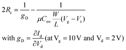
Two main routes have been developed to enhance the electrical performance of SiNW FETs by reducing contact resistance. The first one is to generate metal silicide contacts which reduce the parasitic resistance and improve device and circuit performances.20–23 The second one is to tune the level of doping along the axis of the SiNWs to afford conductive silicon areas.24,25 Our strategy, also recently developed by Mayer et al.,25 is to improve carrier injection by decreasing the contact resistance thanks to high doping at both ends of the SiNWs. Indeed, it is well known that contact resistance is negligible for the measurement of transconductance in heavily doped SiNW devices, while it makes a substantial contribution in lightly doped SiNW devices.9 For two-probe contact analysis, the total resistance is Rt = 2Rc + Rall![[hair space]](https://www.rsc.org/images/entities/char_200a.gif) SiNWs where 2Rc is the contact resistance at the source and drain electrodes, and RallSiNWs corresponds to the resistance of all the nanowires bridging the channel. For a single SiNW, RSiNW = Rundoped + 2Rhighly doped with R = ρLS−1 where ρ is the nanowire resistivity, L is the length of the active part of the nanowire and S the area of the nanowire section. The resistivities of undoped and doped (P:Si = 2 × 10⁻²) SiNWs reported in a previous work15 were respectively 44.4 Ω cm and 3.56 × 10⁻⁴ Ω cm, corresponding to doping concentrations of 1 × 10¹⁴ at cm−3 and 2 × 10¹⁹ at cm−3. It implies that Rundoped ≫ Rhighly doped thus RSiNW ≈ Rundoped. For instance, a 50 nm in diameter and 1 μm long SiNW has a resistance of Rundoped = 2.3 × 10⁸ Ω. In the devices, several SiNWs bridge the channel, acting as parallel resistors. The inverse of RallSiNWs is equivalent to n/Rundoped where n is the number of nanowires bridging the channel. No more than 5 SiNWs were connected between electrodes, which means that RallSiNWs could be estimated around 46 MΩ to 77 MΩ depending on the number of nanowires connecting the source and drain electrodes. From the FET characteristics, 2Rc values were calculated according to eqn (1) proposed by Jain:26,27
SiNWs where 2Rc is the contact resistance at the source and drain electrodes, and RallSiNWs corresponds to the resistance of all the nanowires bridging the channel. For a single SiNW, RSiNW = Rundoped + 2Rhighly doped with R = ρLS−1 where ρ is the nanowire resistivity, L is the length of the active part of the nanowire and S the area of the nanowire section. The resistivities of undoped and doped (P:Si = 2 × 10⁻²) SiNWs reported in a previous work15 were respectively 44.4 Ω cm and 3.56 × 10⁻⁴ Ω cm, corresponding to doping concentrations of 1 × 10¹⁴ at cm−3 and 2 × 10¹⁹ at cm−3. It implies that Rundoped ≫ Rhighly doped thus RSiNW ≈ Rundoped. For instance, a 50 nm in diameter and 1 μm long SiNW has a resistance of Rundoped = 2.3 × 10⁸ Ω. In the devices, several SiNWs bridge the channel, acting as parallel resistors. The inverse of RallSiNWs is equivalent to n/Rundoped where n is the number of nanowires bridging the channel. No more than 5 SiNWs were connected between electrodes, which means that RallSiNWs could be estimated around 46 MΩ to 77 MΩ depending on the number of nanowires connecting the source and drain electrodes. From the FET characteristics, 2Rc values were calculated according to eqn (1) proposed by Jain:26,27
 | (1) |
The different parts of the axially doped SiNWs were characterized and measured by scanning spreading resistance microscopy (SSRM) using a Dimension 3100 microscope from Veeco instruments. SSRM is an AFM-mode that maps simultaneously the topography and the local resistivity of the sample (Fig. 1).
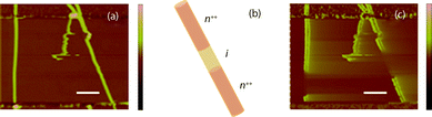 | ||
| Fig. 1 SSRM measurements performed on SiNWs bridged at both ends by two Ni pads, with characteristic pictures of (a) topography (Δz = 200 nm) and (c) resistivity mapping (ΔV = 20 V); scale bar is 1μm. (b) Schematic view of SiNWs axially doped at both ends. | ||
Measurements were carried out with a 1 V source–drain bias and the use of a diamond-coated metallic tip. Fig. 1(a) depicts the topography of two NWs bridging the Ni electrodes (after thermal silicidation as previously described). Fig. 1(c) shows the electrical response correlated to the height image [Fig. 1(a)]. Two equivalent conductive parts are measured at both ends of the SiNWs, and a resistive internal part of 1.0 μm corresponding to the non-intentionally doped segment can be easily observed. The two conductive parts of the SiNWs correspond actually to the highly n-doped part and not to Ni silicides which are only few tens of nanometres long as observed by SEM (see Fig. 2 inset). The lengths of sections along the SiNWs axis measured by SSRM were in good agreement with the experimental parameters used during the VLS synthesis.
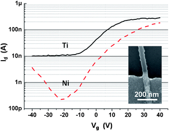 | ||
| Fig. 2 Transfer curves IdversusVg at Vd = 2 V for transistors having Ti (black solid line, not annealed) or Ni (red dashed line, annealed) electrodes on non-flexible substrate. Inset: SEM image of the Ni silicide. | ||
The number of SiNWs transferred and connected between the source and drain electrodes was roughly controlled by the pressure applied during the contact printing and then precisely measured by SEM. Representative transfer curves for SiNW FET fabricated on non flexible substrate with Ti or Ni electrodes are compared in Fig. 2.
For devices with nickel silicide, the FETs show an ambipolar behaviour, i.e. hole injection occurs for negative gate voltages and electron injection occurs for positive gate biases. Similar electronic transport for SiNW FETs was previously reported by Fisher et al. who clearly pointed out a transition from p-type enhancement mode FET to an ambipolar SiNW FET through nichrome gold contact annealing.29 Colli et al. also investigated the electronic transport in ambipolar SiNWs as a function of the electrode metal.18 Ti or Ni contacts on SiNWs and rapid thermal annealing were evaluated in terms of contact resistance and band alignment. They observed that annealed Ni contacts yield the lowest device resistance and highest on/off ratio.
The effective mobilities of the FET (Table 1) were extracted from the measured transconductance  of the current–voltage characteristics according to eqn (2) at Vd = 2 V:
 | (2) |
| Devices [substrate/pad] | μ /cm2 V−1 s−1 | I on/Ioff | I off/A | V t/V | Charge carriers |
|---|---|---|---|---|---|
| Si/Ni | 4.8 | 5.8 × 10² | 4.1 × 10⁻¹⁰ | 10.0 | e− |
| 1.0 × 10⁻² | 8.9 | 4.2 × 10⁻¹⁰ | −25.0 | h+ | |
| Si/Ti | 12.6 | 4 × 101 | 7.4 × 10⁻⁹ | −2.0 | e− |
| — | — | — | — | h+ | |
| PEN/Ti | 101.0 | 1.2 × 10⁷ | 2.0 × 10⁻¹⁴ | 14.3 | e− |
| 4.0 × 10⁻⁴ | 2.4 × 10⁴ | 2.0 × 10⁻¹⁴ | −33.3 | h+ |
Fig. 2 clearly shows that FETs with Ti contacts seem to lose their ambipolar behaviour on non-flexible substrates, in agreement with published results.18 The observed residual plateau can be ascribed to thermoionic emission.31 For Ni contacts an off state is clearly measured (Ioff = 2 × 10⁻¹⁰ A). The lack of thermoionic emission in Ni-based devices may be related to a different SB between the metal and the SiNWs. Indeed, SB energy (for holes) is about 0.08 eV using Ti31 whereas SB (for holes) between Ni and SiNW is 0.57 eV.32 The Ion increase between the two devices is mainly due to the number of silicon nanowires connected between the source and drain. Effective electron mobilities are respectively 5 and 12 cm2 V−1 s−1 for Ni and Ti contacts, in the same range but lower than the 28 cm2 V−1 s−1 recently reported for axially doped SiNW FETs on non-flexible substrates.25
In the second part of this study, the same SiNWs were transferred onto flexible substrates to evaluate the performances of flexible SiNW FETs. Poly(ethylenenaphthalate) (PEN) films TEONEX® Q65 were used as the flexible substrates. Gold (60 nm) was evaporated onto the films to form the gate electrode, then 800 nm of UV crosslinkable organic dielectric was spin-coated. SiNWs were transferred from their growth substrate onto the device (vide supra) and Ti or Ni-based source and drain electrodes were evaporated using optical lithography and a lift-off process. A schematic view and image of a flexible SiNW FET are presented in Fig. 3.
Due to low thermal stability of flexible substrate, no thermal annealing was carried out thereafter and thus no silicidation could be performed. Consequently, no functional transistors were obtained with Ni contacts as already reported by Byon et al. on non-flexible substrate,29 but transistors were achieved for Ti electrodes. Transfer curves of FET using Ti electrodes on both flexible and non-flexible substrates are presented in Fig. 4.
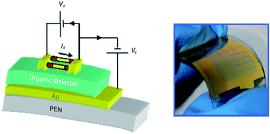 | ||
| Fig. 3 Stacking schematic view of a flexible FET having axially end-doped SiNWs in the channel, and image of a flexible device containing more than 50 linear transistors. | ||
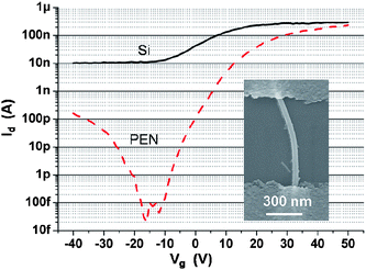 | ||
| Fig. 4 High-performance ambipolar SiNW device on plastic. Comparison of transfer curves (Vd = 2 V) of non-flexible SiNW FET (black solid line) and flexible ambipolar SiNW FET (red dashed line) having both Ti pads as source and drain electrodes. Inset: SEM image of a SiNW in a flexible device connected between Ti electrodes with no thermal annealing. | ||
For Ti contacts realised under identical processes, SiNW FET performance appears to be strongly substrate dependent. Flexible devices showed an ambipolar behaviour with a very low off current (Ioff <5 × 10⁻¹⁴ A). Electrical values presented in Table 1 point out an on/off ratio higher than 107, which is to our knowledge the highest value reported to date for flexible SiNW FETs. Moreover, an effective electron mobility ranging from 72 up to 124 cm2 V−1 s−1 was measured on five devices, which is also a very promising result though non-negligible variation (101 cm2 V−1 s−1 ± 28% for μ values) was observed. Although we have no clear explanation for such a difference between flexible and non-flexible substrates, all these results are very encouraging when compared to the literature.12,13,25,33,34 It is likely that surface potential at the organic dielectric/SiNW and SiO2/SiNW interfaces are quite different due to differences in interface charges, interface energetics and interface dipoles. Moreover, it is known that Schottky barrier height at the source and drain contacts is tuned by surface potential Ψs.35–37 Thus, different behaviours of SiNW FET devices on flexible and non-flexible substrates might be related to the modification of the Ti work function due to the dielectric nature which can significantly influence the surface potential near the bottom of the electrode and at the dielectric/SiNW interface. Further experiments are ongoing to investigate this issue.
Conclusion
In summary, a specific n-doped profile along the axis of SiNWs was designed by a VLS growth process. Integration of these heterostructured SiNWs by a bottom-up approach into FET has been performed on both non-flexible and flexible substrates. The SSRM technique allowed us to visualize and characterize the intrinsic or unintentionally doped part in between the highly doped ends. Ti-based SiNW devices were fabricated on flexible substrates at low temperature. They showed an ambipolar behaviour. Furthermore on/off ratios exceeding 107 and electron mobilities of 124 cm2 V−1 s−1 were measured. These performances are among the highest reported values in the literature for SiNW-based flexible devices. We hope the methods presented here should be applicable to more complex circuits such as OLED drivers or flexible sensors, and could be a useful direction for future development of macroelectronics based on SiNW FETs.Acknowledgements
This research was supported partly by the European integrated project Hydromel NMP2-CT-2006-026622. The authors would like to acknowledge Dr D. Vuillaume for valuable discussions and Dr M. Heitzmann and S. Poncet for their help.References
- X. Duan, MRS Bull., 2007, 32, 134–141 CAS.
- A. J. Baca, J. H. Ahn, Y. Sun, M. A. Meitl, E. Menard, H. S. Kim, W. M. Choi, D. H. Kim, Y. Huang and J. A. Rogers, Angew. Chem., Int. Ed., 2008, 47, 5524–5542 CrossRef CAS.
- T. Sekitani, H. Nakajima, H. Maeda, T. Fukushima, T. Aida, K. Hata and T. Someya, Nat. Mater., 2009, 8, 494–499 CrossRef CAS.
- D.-H. Kim, J.-H. Ahn, W. M. Choi, H.-S. Kim, T.-H. Kim, J. Song, Y. Y. Huang, Z. Liu, C. Lu and J. A. Rogers, Science, 2008, 320, 507–511 CrossRef CAS.
- S. Logothetidis, Mater. Sci. Eng., B, 2008, 152, 96–104 CrossRef CAS.
- R. A. Street, Adv. Mater., 2009, 21, 2007–2022 CrossRef CAS.
- E.-A. Chung, J. Koo, M. Lee, D.-Y. Jeong and S. Kim, Small, 2009, 5, 1821–1824 CrossRef CAS.
- T. N. Ng, S. W. William, A. L. Rene and A. S. Robert, Adv. Mater., 2009, 21, 1855–1859 CrossRef CAS.
- X. Wu, J. S. Kulkarni, G. Collins, N. Petkov, x. Alme, D. cija, J. J. Boland, D. Erts and J. D. Holmes, Chem. Mater., 2008, 20, 5954–5967 CrossRef CAS.
- G. Yu, A. Cao and C. M. Lieber, Nat. Nanotechnol., 2007, 2, 372–377 CrossRef CAS.
- W. Lu, P. Xie and C. M. Lieber, IEEE Trans. Electron Devices, 2008, 55, 2859–2876 CrossRef CAS.
- X. Duan, C. Niu, V. Sahi, J. Chen, J. W. Parce, S. Empedocles and J. L. Goldman, Nature, 2003, 425, 274–278 CrossRef CAS.
- M. C. McAlpine, R. S. Friedman, S. Jin, K.-h. Lin, W. U. Wang and C. M. Lieber, Nano Lett., 2003, 3, 1531–1535 CrossRef CAS.
- L. Latu-Romain, C. Mouchet, C. Cayron, E. Rouviere and J. P. Simonato, J. Nanopart. Res., 2008, 10, 1287–1291 CrossRef CAS.
- C. Cayron, M. Den Hertog, L. Latu-Romain, C. Mouchet, C. Secouard, J.-L. Rouviere, E. Rouviere and J.-P. Simonato, J. Appl. Crystallogr., 2009, 42, 242–252 CrossRef CAS.
- C. Celle, C. Mouchet, E. Rouvière, J.-P. Simonato, D. Mariolle, N. Chevalier and A. Brioude, J. Phys. Chem. C, 2010, 114, 760–765 CrossRef CAS.
- A. Javey, Nam, R. S. Friedman, H. Yan and C. M. Lieber, Nano Lett., 2007, 7, 773–777 CrossRef CAS.
- A. Colli, S. Pisana, A. Fasoli, J. Robertson and A. C. Ferrari, Phys. Status Solidi B, 2007, 244, 4161–4164 CrossRef CAS.
- L. J. Chen, Silicide Technology for Integrated Circuits, The Institution of Engineering and Technology, London, 2004 Search PubMed.
- W. M. Weber, L. Geelhaar, A. P. Graham, E. Unger, G. S. Duesberg, M. Liebau, W. Pamler, C. Cheze, H. Riechert, P. Lugli and F. Kreupl, Nano Lett., 2006, 6, 2660–2666 CrossRef CAS.
- Y.-C. Lin, K.-C. Lu, W.-W. Wu, J. Bai, L. J. Chen, K. N. Tu and Y. Huang, Nano Lett., 2008, 8, 913–918 CrossRef CAS.
- S. M. Sze, Semiconductor Devices: Physics and Technology, John Wiley & Sons, New York, 2nd edn, 2002 Search PubMed.
- A. L. Schmitt, J. M. Higgins, J. R. Szczech and S. Jin, J. Mater. Chem., 2010, 20, 223 RSC.
- H. Schmid, M. T. Bjork, J. Knoch, S. Karg, H. Riel and W. Riess, Nano Lett., 2009, 9, 173–177 CrossRef CAS.
- T. T. Ho, Y. F. Wang, S. Eichfeld, K. K. Lew, B. Z. Liu, S. E. Mohney, J. M. Redwing and T. S. Mayer, Nano Lett., 2008, 8, 4359–4364 CrossRef CAS.
- J. Collet, O. Tharaud, A. Chapoton and D. Vuillaume, Appl. Phys. Lett., 2000, 76, 1941–1943 CrossRef CAS.
- S. Jain, IEEE Proc., 1988, 135, 162–164.
- G. Jing, W. Jing, E. Polizzi, S. Datta and M. Lundstrom, IEEE Trans. Nanotechnol., 2003, 2, 329–334 CrossRef.
- K. Byon, D. Tham, J. E. Fischer and A. T. Johnson, Appl. Phys. Lett., 2007, 90, 143513 CrossRef.
- W. Lu, P. Xie and C. M. Lieber, IEEE Trans. Electron Devices, 2008, 55, 2859–2876 CrossRef CAS.
- A. Colli, A. Fasoli, P. Beecher, P. Servati, S. Pisana, Y. Fu, A. J. Flewitt, W. I. Milne, J. Robertson, C. Ducati, S. De Franceschi, S. Hofmann and A. C. Ferrari, J. Appl. Phys., 2007, 102, 034302 CrossRef.
- Y. Ahn, J. Dunning and J. Park, Nano Lett., 2005, 5, 1367–1370 CrossRef CAS.
- B. Salem, F. Dhalluin, H. Abed, T. Baron, P. Gentile, N. Pauc and P. Ferret, Solid State Commun., 2009, 149, 799–801 CrossRef CAS.
- A. Colli, A. Tahraoui, A. Fasoli, J. M. Kivioja, W. I. Milne and A. C. Ferrari, ACS Nano, 2009, 3, 1587–1593 CrossRef CAS.
- J. Collet and D. Vuillaume, Appl. Phys. Lett., 1998, 73, 2681–2683 CrossRef CAS.
- R. T. Tung, Mater. Sci. Eng., R, 2001, 35, 1–138 CrossRef.
- S. G. J. Mathijssen, M. Kemerink, A. Sharma, M. Cölle, P. A. Bobbert, R. A. J. Janssen and D. M. de Leeuw, Adv. Mater., 2008, 20, 975–979 CrossRef CAS.
| This journal is © The Royal Society of Chemistry 2010 |