Pinning of organic nanofiber surface growth
Roana Melina
de Oliveira Hansen
*,
Jakob
Kjelstrup-Hansen
and
Horst-Günter
Rubahn
NanoSYD, Mads Clausen Institute, University of Southern Denmark, Alsion 2, DK-6400 Sønderborg, Denmark. E-mail: roana@mci.sdu.dk
First published on 6th October 2009
Abstract
In situ growth constitutes a very promising strategy for integrating functional nanostructures into device platforms due to the possibility of parallel, high-volume integration. Here, we demonstrate how electron-beam-lithography-defined metal nanostructures can be used to guide the surface diffusion and thereby steer the self-assembly process of organic molecules (here para-hexaphenylene) leading to morphologically well-defined molecular nanofibers with preferred growth directions. Results from a systematic investigation of the influence of the nanofiber growth parameters (such as pinning structure dimensions, substrate temperature, etc.) are presented and an appropriate parameter set is found that enables control over nanofiber length, position and orientation. The ability to achieve such parallel growth control opens a wide range of possible applications including fabrication of polarization-controlled light-emitting arrays and nanofiber growth between electrodes for direct electrical connection in organic LEDs.
Introduction
The combination of bottom-up and top-down technologies leads to a range of new device functionalities by integrating new materials into conventional silicon microsystem technology. For example, optoelectronic devices, which are often difficult to realize in silicon due to its indirect bandgap, can be made possible by integration of nanowires made from inorganic semiconductors such as III–V or II–VI materials with direct bandgaps.1 This has made possible both active2–4 and passive5 optoelectronic and photonic components such as LEDs, lasers, photodetectors, and waveguides. In addition, such nanostructures can function as advanced bio-sensors based on evanescent wave sensing due to their sub-wavelength cross-sectional dimensions.6Typically, the integration of inorganicnanowires into silicon technology is done by first fabricating the nanowires on an appropriate growth substrate, followed by a transfer process to the silicon platform and additional processing to create the necessary interface.4,7 Although large-scale assembly has recently been demonstrated with such methodology,4 it is restricted to planar geometries and requires the use of special donor substrates. An alternative technique is in situ growth, in which the nanowires are fabricated directly on the silicon substrate typically using catalystnanoparticles to define nanowire diameter and position.8 Despite problems regarding lattice mismatch and differences in crystal structure and thermal expansion coefficients, III–Vnanowires can be grown epitaxially on silicon9 enabling, for example, nanowire LEDs.10
Inorganic materials offer only limited design flexibility as compared to their organic counterparts, which through synthetic chemistry methods can be tailored for a particular application.11,12 It has been shown that organic semiconductors can be formed into nanoscale, elongated, crystalline structures – ‘nanofibers’ – through bottom-up methods.13,14 For example, para-hexaphenylene (p6P) molecules can self-assemble into lateral nanofiber structures by physical vapor deposition onto a heated mica substrate.13 Such p6P nanofibers exhibit a range of functional properties such as emission of polarized, blue light through photoluminescence,15 waveguiding,16 and lasing,17 while electrical connection to the nanofibers18 could enable OLED applications. In addition, by modifying the molecular building blocks, the nanofiber properties can be engineered for a particular application, for example tuning of the emission spectrum15 or color conversion through frequency doubling.19
Alternative methods for obtaining elongated, organic nanostructures exist such as electrospinning20–22 and template wetting.23Electrospinning uses electrical forces to create polymer fibers with diameters in the range of 40–2000 nm.20 When electrical forces on free charges on the surface or inside a polymer material resting on a sharp conductive tip overcome the surface tension, it causes an electrically charged jet to be emitted. This jet solidifies and an electrically charged fiber can be collected at an appropriate device platform. This method can also enable the fabrication of light-emitting nanofibers,21,22 which, however, are polymer-based (i.e. non-crystalline) and cannot be fabricated in situ. A method based on wetting of porous alumina templates also exists23 but suffers from some of the same drawbacks in terms of lacking crystallinity and in situ growth possibilities.
The standard substrate for p6P nanofiber growth is the mineral muscovite mica.13 On this substrate, a dipole-induced dipole interaction between the molecules and the substrate causes the nanofibers to grow along one of the high-symmetry directions of the mica surface, and the nanofibers are therefore straight and mutually parallel. However, as further processing of mica is not practical, the nanofibers need to be transferred to another platform for device applications, conceptually similar to the transfer strategy for the inorganicnanowires. However, large-scale device fabrication requires efficient placement and integration methods, which are, up to now, missing for organic nanofibers due to the soft and fragile nature of such van der Waals-bonded molecular crystals.24In situ growth would therefore constitute a highly interesting alternative. This requires that a suitable growth substrate is identified and a method for nanofiber growth control is developed. It has been shown that thin gold films constitute an alternative nanofiber growth platform, albeit without mutual alignment of the nanofibers.25 If the substrate surface is structured on the micrometre scale, however, the nanofiber growth orientation will be affected by the microstructures.26 The use of gold-coated silicon platforms as the growth substrate is very beneficial, since the processing technology for silicon structuring is highly developed and advanced growth substrates can therefore be fabricated.
In the present work we go a step further and use ultrathin, nanoscale titanium lines on a gold-coated silicon substrate as pinning structures, thus avoiding the necessity to fabricate grooves into the substrates. The pinning lines are fabricated by electron-beam lithography, titanium deposition and lift-off, and nanofibers are grown on the substrate by physical vapor deposition of the p6P molecules. We present results from a systematic investigation of the influence of various processing parameters such as pinning-line dimensions, pitch distance, substrate temperature and p6P thickness on the nanofiber alignment, length and position control. From this study we determine optimum parameters for pinning of the growth.
Results and discussion
Upon deposition of p6P molecules on the nanostructured substrates, the nanofibers were investigated with scanning electron microscopy (SEM). Figs. 1a and b show SEM images of nanofibers grown on a gold film by deposition of 4 nm p6P at substrate temperatures of 418 K (Fig. 1a) and 448 K (Fig. 1b), respectively. The pinning lines have a width of 250 nm and a height of 25 nm. The pitch distance varies between 2.5 µm (label ‘1’ in Fig. 1a) and 17.5 µm (label ‘7’). The deposited p6P molecules undergo diffusional motion on the heated gold surface until they reach a pinning line, causing the nanofibers to grow from the line. Different deposition conditions such as different substrate temperatures lead to distinct differences in the orientation and morphology of the resulting nanofibers. As observed from the SEM images, the fibers grow longer if the deposition is performed at a higher substrate temperature since the diffusional range is increased. The nanofiber length is also influenced by the pinning line pitch distance. Under appropriate conditions, the nanofibers bridge between two lines and length control can thereby be achieved as shown in Fig. 2. | ||
| Fig. 1 (a and b) SEM images of p6P nanofibers grown on sputtered gold with titanium pinning lines (width of 250 nm and height of 25 nm) at substrate temperatures of 418 K (a) and 448 K (b), respectively. The distances between the lines are 2.5 µm (1), 5 µm (2) … 17.5 µm (7); (c and d) orientational distributions for the fibers growing between lines at a pitch distance of 10 µm (4) for substrate temperatures of 418 K (c) and 448 K (d), respectively. Here, 90 degrees refers to the long fiber axes being perpendicular to the pinning lines. | ||
 | ||
| Fig. 2 SEM image of a nanofiber bridge between two pinning lines (width of 250 nm and height of 50 nm) at a pitch distance of 2.5 µm. The substrate temperature during deposition of 4 nm p6P was 433 K. | ||
The fiber orientation is another characteristic property affected by the growth conditions. The fibers grown on a high-temperature substrate exhibit a better alignment, i.e. they grow more perpendicular to the pinning lines. This effect has been observed also for nanofibers growing on or between microstructures.26 At high temperatures, most fibers grow from the pinning lines even for long pitch distances. At lower temperatures and long pitch distances, some fibers nucleate inbetween and are thereby disconnected from the lines, which results in a decrease of the alignment factor.
Systematic analyses with the objective of obtaining quantitative data for the fibers’ alignment were made by measuring their angle with respect to the pinning line direction. 90° refers to fibers oriented perpendicularly to the pinning lines. The orientational distributions corresponding to the fibers grown at a pitch distance of 10 µm (label ‘4’ in Fig. 1a) at 418 K and at 448 K are plotted in Figs. 1c and d, respectively. As seen, the width of the distribution is narrower for fibers grown at a high temperature as compared to those grown at a low temperature.
Another factor affecting the nanofiber growth is the quality of the gold, which is influenced by the deposition method. Figs. 3a and b show SEM images of nanofibers grown from titanium pinning lines on a gold film that had been deposited by either DC sputtering or electron-beam evaporation, respectively, while Fig. 3c shows a SEM image of nanofibers grown on a sputter-deposited gold film without pinning lines (4 nm p6P deposition, substrate temperature of 418 K). The pinning line dimensions are the same as in Fig. 1.
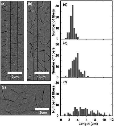 | ||
| Fig. 3 (a and b) SEM image of p6P nanofibers grown on sputtered (a) and electron-beam evaporated (b) gold films with titanium pinning lines (width 250 nm and height 50 nm), respectively, at a substrate temperature of 418 K; (c) SEM image of p6P nanofibers grown on a sputtered gold film without pinning lines at a substrate temperature of 418 K; (d–f) length distribution for the fibers grown between pinning lines (separation 2.5 µm) on the samples shown in (a and b) and for the substrate shown in (c), respectively. | ||
The nanofiber lengths for the fibers grown between the 2.5 µm pitch distance lines for the samples presented in Figs. 3a and b are plotted in the histograms in Figs. 3d and e, respectively, while the length distribution on the unstructured film is shown in Fig. 3f. The distributions illustrate that the pinning lines are indeed limiting the nanofiber lengths on both types of gold film, but the effect is more pronounced on the gold film that was deposited by sputtering. A better alignment to the pinning lines is observed on the sputter deposited film, while on the film deposited by evaporation, more fibers are not perpendicular to the pinning lines, making it possible for them to grow longer. Fig. 4 shows 3D AFM images of 60 nm of Au deposited on Si by sputtering (4a) and by electron-beam evaporation (4b). The maximum z-range is 3.8 nm. An analysis of the surface roughness shows that the evaporated gold film has a 20% larger surface roughness than the sputtered film. We propose that this is affecting the diffusional motion of the molecules and that it could cause the observed difference in alignment.
 | ||
| Fig. 4 AFM images of a 60 nm Au film deposited on Si by (a) sputtering and (b) electon-beam evaporation. | ||
The ability of the pinning lines to control the nanofiber length is also demonstrated in Fig. 3. In order to compare to nanofibers grown on an unstructured gold film, Fig. 3c displays such nanofibers grown under the same conditions as the fibers in Fig. 3a. The length distribution for these fibers is very wide (Fig. 3f), since this is a statistical process without any limiting factors and there is therefore no length control. An improvement in length control can be seen by comparing Figs. 3d and f, where the length distribution is significantly narrower for the former case.
Fig. 5 shows how the various processing parameters affect the nanofibers. In the first row, the average lengths for the fibers are shown with the different processing parameters varied on the five columns. The fiber orientation as a function of the parameters is plotted in the second row. Here, it is plotted as 100 divided by the standard deviation of the orientational distribution. In this way, the fiber orientation factor is increasing when the alignment is improved. The characteristic shown in the last row is the position control or pinning factor, which is defined as:
| PC = Nc/(Nnc + Nc) |
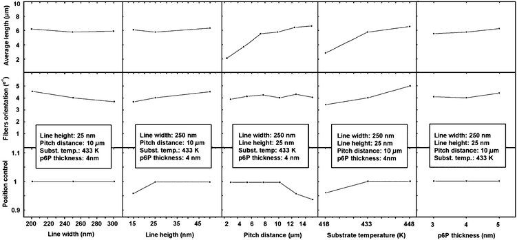 | ||
| Fig. 5 Nanofiber average length, orientation, and position control as a function of substrate and growth parameters. | ||
As observed from the first column, the line width does not have a significant influence on most of the parameters, except for a slightly decreasing fiber orientation for increasing line width. The opposite trend is observed for increasing line height (second column), in which case the fibers exhibit a better orientation. This indicates that the optimum conditions are lines with a large aspect ratio. The pitch distance factor is crucial for the nanofiber length as well for the position control, since for large areas inbetween pinning lines, some of the molecules do not have sufficient thermal energy to diffuse to the lines, and fibers are grown disconnected from the lines. The effect of the pitch distance is to determine the average length of the nanofibers, since the fiber lengths are limited by the available space inbetween two pinning lines. If the pitch distance is small enough, length control can be achieved.
The substrate temperature is an essential parameter since it influences length, alignment and position control, while the p6P thickness does not have a significant influence. It has been shown that there is a maximum substrate temperature for nanofiber growth, which is around 450 K.26 At the highest temperature used here (448 K), the standard deviation of the orientational distribution is 19°. This could be compared to nanofibers grown on mica, in which the epitaxial relation with the substrate causes a mutual alignment of the nanofibers with a standard deviation of the angular distribution of just 1.2°.25,27 However, as previously noted, any processing on mica is practically impossible, rendering the silicon-based platform the preferred choice for in situ growth experiments despite the inferior nanofiber alignment properties. In addition, the use of pinning lines also enables length control on the silicon-based platform, which is not possible on plain mica, where the length distribution function is similar to that on plain Au (see above).
The p6P molecules emit blue light upon UV excitation with the emitted photons polarized along the long molecular axis. In the nanofiber crystal structure, the molecules are mutually parallel and aligned almost perpendicular to the long nanofiber axis.13 The photoluminescence output from the nanofibers is therefore also polarized approximately perpendicular to the long nanofiber axis. Fig. 6 illustrates how this property causes the emitted light from the aligned nanofibers to be polarized.
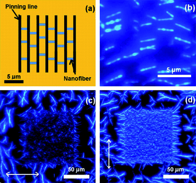 | ||
| Fig. 6 (a) Outline of sample geometry: parallel pinning lines (width of 250 nm and height of 25 nm) with a pitch distance of 2.5 µm; (b) fluorescence microscopy images of p6P nanofibers grown at substrate temperature of 433 K; (c and d) The nanofibers are illuminated with unpolarized light and imaged through a polarizer. The polarizer direction is parallel (c) and perpendicular (d) to the long lines axis as indicated by the arrows. | ||
The nanofibers are grown on an array of pinning lines with a pitch distance of 2.5 µm, as illustrated in Fig. 6a. The pinning lines are vertical with a width of 250 nm while their heights are 25 nm. The deposition of 4 nm p6P was performed at a substrate temperature of 433 K, forming nanofibers perpendicular to the lines, as shown in Fig. 6b. Figs. 6c and d show epifluorescence microscopy images of nanofibers illuminated with unpolarized light and imaged through a polarizer. In Fig. 6c, the polarizer direction is horizontal while in Fig. 6d the direction is vertical. When the polarizer is rotated for observation of light polarized approximately parallel to the long nanofiber axes, only minor light emission is observed, however, rotating the polarizer by 90° causes a significant increase in the observed light intensity. This indicates that the light-emitting molecules are oriented all perpendicular to the long nanofiber axes and thus parallel to the pinning lines. The pinning lines thus allow one to fabricate areas with well defined polarization on samples that otherwise emit unpolarized light.
Experimental
Substrate preparation
The nanofiber growth platform consists of silicon (100) substrates, which initially were coated with a 5 nm Ti adhesion layer deposited by electron-beam deposition and a 60 nm thick Au film deposited by electron-beam deposition (rate: 2 Å s−1, background pressure in the 10−6 mbar range) or by DC sputtering (rate: 5 Å s−1, pressure in the 10−3 mbar range). Nanoscale titanium lines were fabricated by electron-beam lithography, titanium deposition, and lift-off: 150 nm PMMA was applied by spin coating, and the electron-beam lithography was performed at 30 keV in a Hitachi S-4800 SEM with a Raith ELPHY Quantum module. After exposure, the pattern was developed by immersion in a 3 : 1 IPA:MIBK solution, rinsed, and dried, followed by Ti deposition (rate 1 Å s−1, background pressure in the 10−6 mbar range). Different thicknesses of Ti were used in order to study the Ti height influence. The resist was lifted-off by immersing the samples in a Remover PG solution and applying ultrasonic agitation. Before deposition of p6P molecules, the samples were cleaned with a mild oxygen plasma to remove any organic residues.Nanofiber growth
Organic nanofibers were grown on the nanostructured substrates by physical vapour deposition of p6P molecules at a rate of 0.1 Å s−1. During deposition, the substrate was heated to temperatures in the range 418–448 K and the deposition was performed under high vacuum conditions (10−8 mbar). The organic material is deposited from a Knudsen cell, and the p6P thickness was changed from sample to sample to study its influence on growth control.Characterization
The samples were characterized by scanning electron microscopy (SEM) and epifluorescence microscopy (excitation wavelength of 365 nm).Conclusions
By use of ultrathin titanium lines on gold films, a method for controlling the length, position and orientation of substrate-grown, crystalline organic nanofibers has been developed. Substrate and growth parameters were varied to find the optimum nanofiber growth conditions. Nanofiber growth control is influenced by the gold film deposition method with sputtering providing better oriented fibers than electron-beam evaporation. This is most probably due to the difference in surface roughness between the two gold films, as this will influence the molecular diffusion. Better orientation is obtained for higher aspect ratios of the pinning lines, since taller lines are more difficult to bridge and are thus more effectively stopping the diffusion and creating nucleation centers from where the fibers start to grow. At high temperatures, the fibers are long and straight and can bridge between two lines even at long pitch distances since the diffusion coefficient is increased.The pinning line method relies on general growth parameters such as diffusion properties of the organic molecules on the substrate. It thus requires appropriate surface energetics (e.g., a Au surface is appropriate), but no specific adsorbate/substrate crystalline relationships. The method is thus not limited to the present case of para-hexaphenylene molecules, but should be applicable to all functionalized organic molecules that show nanofiber growth.14
As an extension of the present work, a more accurate growth control might be achieved in the future by designing the pinning lines in special forms, including micro- and nanostructures in the lines or dots. Finally, large-scale growth could be achieved by scaling up the pinning line fabrication by nanoimprint lithography.
Acknowledgements
The authors thank Morten Madsen for valuable discussions. This work was financially supported by the Danish Council for Technology and Innovation through the Octopus innovation consortium. We also thank the Danish Research Council for continued financial support.References
- R. Agarwal and C. M. Lieber, Appl. Phys. A: Mater. Sci. Process., 2006, 85, 209–215 CrossRef.
- E. Lai, W. Kim and P. Yang, Nano Res., 2008, 1, 123–128 Search PubMed.
- X. Duan, Y. Huang, R. Agarwal and C. M. Lieber, Nature, 2003, 421, 241–245 CrossRef CAS.
- Z. Fan, J. C. Ho, Z. A. Jacobson, H. Razavi and A. Javey, Proc. Natl. Acad. Sci. U. S. A., 2008, 105, 11066–11070 CrossRef CAS.
- D. J. Sirbuly, M. Law, P. Pauzauskie, H. Yan, A. V. Maslov, K. Knutsen, C.-Z. Ning, R. J. Saykally and P. Yang, Proc. Natl. Acad. Sci. U. S. A., 2005, 102, 7800–7805 CrossRef CAS.
- D. J. Sirbuly, A. Tao, M. Law, R. Fan and P. Yang, Adv. Mater., 2007, 19, 61–66 CrossRef CAS.
- Y. Huang, X. Duan, Q. Wei and C. M. Lieber, Science, 2001, 291, 630–633 CrossRef CAS.
- T. Mårtensson, M. Borgström, W. Seifert, B. J. Ohlsson and L. Samuelson, Nanotechnology, 2003, 14, 1255–1258 CrossRef CAS.
- T. Mårtensson, C. P. T. Svensson, B. A. Wacaser, M. W. Larsson, W. Seifert, K. Deppert, A. Gustafsson, L. R. Wallenberg and L. Samuelson, Nano Lett., 2004, 4, 1987–1990 CrossRef CAS.
- C. P. T. Svensson, T. Mårtensson, J. Ttägårdh, C. Larsson, M. Rask, D. Hessman, L. Samuelson and J. Ohlsson, Nanotechnology, 2008, 19, 305201 CrossRef.
- K. Müllen, U. Scherf, in Organic Light Emitting Devices, Wiley-VCH, Weinheim, 2005 Search PubMed.
- H. Hoppe and N. S. Sariciftci, J. Mater. Res., 2004, 19, 1924–1945 CAS.
- F. Balzer and H.-G. Rubahn, Appl. Phys. Lett., 2001, 79, 3860–3862 CrossRef CAS.
- M. Schiek, F. Balzer, K. Al-Shamery, J. R. Brewer, A. Lützen and H.-G. Rubahn, Small, 2008, 4, 176–181 CrossRef CAS.
- M. Schiek, A. Lützen, R. Koch, K. Al-Shamery, F. Balzer, R. Frese and H.-G. Rubahn, Appl. Phys. Lett., 2005, 86, 153107 CrossRef.
- F. Balzer, V. G. Bordo, A. C. Simonsen and H.-G. Rubahn, Phys. Rev. B: Condens. Matter Mater. Phys., 2003, 67, 115408 CrossRef.
- F. Quochi, F. Cordella, A. Mura, G. Bongiovanni, F. Balzer and H.-G. Rubahn, J. Phys. Chem. B, 2005, 109, 21690–21693 CrossRef CAS.
- J. Kjelstrup-Hansen, H. H. Hensichsen, P. Bøggild and H.-G. Rubahn, Thin Solid Films, 2006, 515, 827–830 CrossRef CAS.
- J. Brewer, M. Schiek, A. Lützen, K. Al-Shamery and H.-G. Rubahn, Nano Lett., 2006, 6, 2656–2659 CrossRef CAS.
- D. Reneker and I. Chun, Nanotechnology, 1996, 7, 216–223 CrossRef CAS.
- J. M. Moran-Mirabal, J. D. Slinker, J. A. DeFranco, S. S. Verbridge, R. Ilic, S. Flores-Torres, H. Abruña and G. Malliaras, Nano Lett., 2007, 7(2), 458–463 CrossRef CAS.
- F. Di Benedetto, A. Camposeo, S. Pagliara, E. Mele, L. Persano, R. Stabile, R. Cingolani and D. Pisignano, Nat. Nanotechnol., 2008, 3, 614–619 CrossRef CAS.
- D. O'Carroll, I. Lieberwirth and G. Redmond, Nat. Nanotechnol., 2007, 2, 180–184 CrossRef CAS.
- J. Kjelstrup-Hansen, O. Hansen, H.-G. Rubahn and P. Bøggild, Small, 2006, 2, 660–666 CrossRef CAS.
- F. Balzer, L. Kankate, H. Niehus, R. Frese, C. Maibohm and H.-G. Rubahn, Nanotechnology, 2006, 17, 984–991 CrossRef CAS.
- M. Madsen, J. Kjelstrup-Hansen and H.-G. Rubahn, Nanotechnology, 2009, 20, 115601 CrossRef.
- F. Balzer, private communication, 2009.
| This journal is © The Royal Society of Chemistry 2010 |