TiO2 nanotubes and their application in dye-sensitized solar cells
Poulomi
Roy
a,
Doohun
Kim
a,
Kiyoung
Lee
a,
Erdmann
Spiecker
b and
Patrik
Schmuki
*a
aDepartment of Materials Science, WW4-LKO, University of Erlangen–Nürnberg, Martensstrasse 7, 91058 Erlangen, Germany. E-mail: schmuki@ww.uni-erlangen.de; Fax: +49-9131-852-7582; Tel: +49-9131-852-7575
bDepartment Werkstoffwissenschaften, Lehrstuhl Mikrocharakterisierung/VII, University of Erlangen–Nürnberg, Cauerstraße 6, 91058 Erlangen, Germany
First published on 4th December 2009
Abstract
The present article reviews the current status of using TiO2 nanotubes in Grätzel-type, dye-sensitized solar cells and extends the overview with the latest results and findings. Critical factors in tube geometry (length, diameter, top morphology), crystal structure (amorphous, anatase, rutile) as well as factors affecting dye loading or electron mobility are addressed. The highest solar cell efficiencies today for pure nanotube systems reach approximately 4% while for some mixed systems, around 7% has been reported. For both systems significant room for enhancement is anticipated and some key points and strategies for improvement are outlined.
 Poulomi Roy | Poulomi Roy received her MSc degree in Inorganic Chemistry from Vidyasagar University, India and obtained her PhD degree in Inorganic Nanomaterials from the Indian Institute of Technology, Kharagpur, in 2007. She joined the group of Prof. Patrik Schmuki at the University of Erlangen–Nürnberg, Germany in 2008 as a post-doctoral fellow, where currently she is continuing her research. Her research interests include the synthesis of semiconductor nanomaterials and their application in various energy fields, especially in solar cells. |
 Doohun Kim | Doohun Kim received his MSc degree from Inha University, Inchon, South Korea in 1999. He then worked at Solartech Corp., Seoul for four years. Currently, he is persuing his PhD degree in Prof. Patrik Schmuki’s lab at the University of Erlangen–Nürnberg, Germany. His research interest includes synthesis of self-organized nanomaterials by electrochemical means and their applications in different energy devices. |
 Kiyoung Lee | Kiyoung Lee obtained his MSc degree in Chemical Engineering from Inha University, Korea in 2009. He is currently a PhD student under the supervision of Prof. Schmuki at the University of Erlangen–Nürnberg in Germany. His research interests include functional nanomaterial synthesis by electrochemical methods with the direction of application in energy conversion and storage devices. |
 Erdmann Spiecker | Erdmann Spiecker received his PhD in physics in 1999 from the University of Göttingen. In 2000 he joined the Materials Science Department of the University of Kiel as research associate. He was awarded a Humboldt Fellowship in 2005 and spent over a year at the National Center for Electron Microscopy in Berkeley. In 2007 he received his habilitation from the University of Kiel. Since September 2008 he has been Professor of Materials Science and head of the Electron Microscopy group at the University of Erlangen–Nürnberg. His research focuses on electron microscopy techniques for investigation of nanostructured materials. |
 Patrik Schmuki | Patrik Schmuki studied physical chemistry at the University of Basel, and obtained his PhD degree from ETH-Zurich in 1992. From 1994–97 he worked at Brookhaven National Laboratory, USA and the Institute for Microstructural Sciences of the NRC, Canada. From 1997–2000 he was an Associate Professor for Microstructuring Materials at EPFL, Switzerland, and since 2000 he is Full Professor and head of the Institute for Surface Science at the Materials Science Department of the University of Erlangen–Nürnberg. His current research interests cover electrochemistry and materials at the nanoscale—with particular focus on functional materials and the control of self-assembly. |
1. Introduction
1.1 General overview
Currently the majority of commercial solar cells are made of different solid-state junction devices, usually from silicon. These cells reach light-to-electricity conversion efficiencies of ≈ 20% for multicrystalline and ≈ 25% for monocrystalline silicon at reasonable cost, and thus represent the milestone of terrestrial applications.1 However, several other concepts are explored that are geared to achieve either higher efficiencies, or manufacture at more attractive costs, or are expected to be overall more environmentally friendly. A particularly striking photoelectrochemical concept is based on dye-sensitized TiO2 – it involves neither expensive semiconductor substrates nor high-level processing steps.In 1985, Desilvestro et al.2 reported TiO2 nanoparticles onto which suitable organic molecules (Ru-based complexes) were adsorbed. Such electrodes were active under visible-light irradiation and allowed solar energy to be converted to electricity with a quantum efficiency of 80%.3 Later on, Grätzel and O'Regan extended the concept to a full solar cell,4–6 which is nowadays known as a dye-sensitized solar cell (DSSC). In these DSSCs the hole-transmitting medium is a redox species in an electrolyte, liquid or gel (quasi solid-state). The principle of such a DSSC is described in Fig. 1. The classic DSSC is composed of a layer of nanocrystalline TiO2 particles on a conducting substrate, a platinum counter electrode, and an adsorbed Ru-dye as a sensitizer and an electrolyte. Using such constructions 11% conversion efficiency has been achieved.7 Usually, the TiO2 nanoparticles are deposited on a conducting glass substrate, and sintered to convert the particles to an anatase crystal phase and to improve the electronic conduction between the conductive glass and the TiO2 nanoparticles. On the TiO2 surface adsorbed is a dye, which serves as a light absorber (sensitizer), and is anchored (attached) to the surface of the TiO2 nanoparticles by specific functional groups. A key requirement for the dye is that the LUMO of the dye molecule is energetically positioned slightly higher than the conduction band of TiO2. Under irradiation with sunlight, HOMO–LUMO transitions in the dye occur. Excited electrons can then be injected from the LUMO into the conduction band of the semiconductor electrode (Fig. 1B). For typically used Ru-ligand dyes the electron injection from the dye sensitizer to the conduction band of TiO2 occurs through a metal-to-ligand charge transfer (MLCT) pathway as shown in Fig. 1C.8 The oxidized dye is reduced to its original state by electron donation from the redox couple in the electrolyte. Usually the electrolyte is an organic solvent or ionic liquid containing an I3−/I− redox system. After the I3− ion is oxidized to I−, it regenerates the dye (refills the HOMO levels). The resulting I− species can diffuse to the Pt counter electrode where they are regenerated to I3− by reduction.
 | ||
| Fig. 1 (A) Schematic representation of the principle of a dye-sensitized solar cell. (B) Schematic diagram of the light-induced electron excitation (HOMO–LUMO transition) and injection process from the LUMO of the dye to the conduction band of TiO2. (C) Excited electron transfer from Ru-metal to the TiO2 conduction band occurs by the so-called metal-to-ligand charge transfer pathway (MLCT). | ||
The potential difference under illumination corresponds to the difference between the Fermi level of the electron in the semiconductor electrode and the redox potential of the electrolyte (i.e., this represents the achievable Voc).
However, not only energetic (thermodynamic) considerations are crucial but also the reaction kinetics. The rate constant for electron injection from the conduction band has to be faster than the de-excitation of the dye and the regeneration time constant for the dye has to be sufficiently fast to avoid depletion effects8,9 (Fig. 2A). Generally, the rate-limiting factor is the dynamic competition between the electron transport in the TiO2 and interfacial recombination of electrons. Typically the electron transport time constants in TiO2 nanoparticles are comparably slow (due to a trapping/de-trapping type of electron transport).10,11 Low electron diffusion coefficients within the TiO2 nanoparticles can be due to defects, surface states, grain boundaries etc. that act as electron trapping sites, thus slowing down electron flow, enhancing recombination and thereby diminishing the electron collection at the back contact.12,13 In order to considerably improve this behaviour, recently research has been prompted towards the use of one-dimensional nanostructures of TiO2, such as, nanotubes,14–19nanorods,20–23nanowires24,25etc. These 1D nanostructures are expected to significantly improve the electron transport properties due to a directional smooth electron mobility (limiting random walk in the wide nanocrystalline network) as well as decreased inter-crystalline contacts, thereby accelerating electron transport and lowering the recombination probability as shown in the schematic diagram of Fig. 2B–C.14
 | ||
| Fig. 2 (A) The most relevant kinetic constants involved in the dynamics of the redox processes involving electron injection from the dye into TiO2, dye regeneration, electron transportation and back-transfer of the electrons to the redox medium. The electron diffusion length (Ln) in TiO2, one of the key parameters in DSSCs, depends on the diffusion constant (Dn) and the electron lifetime (τc) (reproduced with permission from ref. 8. Copyright American Chemical Society, 2005). (B) Schematic representation of typical solar cell construction using TiO2 nanotubes grown on a Ti substrate. (C) A comparison of the electron pathways through nanoparticulate and nanotubular structured TiO2 (3D random walk vs. 1D transport). | ||
Various techniques for synthesizing TiO2 nanotubes and other 1D structures have been reported in recent years, such as sol –gel processes, or hydrothermal approaches.26–30 Although comparably high-efficiency solar cells have been produced with these chemically synthesized 1D morphologies of TiO2, a multidirectional orientation of TiO2 nanotubes or nanorods may not ensure the most efficient unidirectional electron flow along the length of a restricted passage towards the back contact. In principle, as long as the nanotube or nanorod systems are ideal i.e., they provide a highly conductive, rapid electron transport, their orientation on the substrate is of minor importance. This, for example, may hold for single crystalline defect-free nanowires. However, many approaches to grow TiO2 nanotubes lead to a polycrystalline material with substantial recombination possibilities along the electron path. In this case the optimally increased rate of electron transport and the higher charge collection efficiencies can only be expected for nanotubes vertically aligned with the conductive substrate. Therefore approaches to produce self-ordered titaniananotubes by anodic oxidation of Ti in adequate electrolyte31,32 have become of a significant interest – the present review will focus on this point in later sections but will first give a brief overview of some general concepts in DSSCs.
1.2 Key factors for DSSCs
More than 2000 papers have been published on dye-sensitized solar cells with the goal of understanding and optimizing key factors, such as, the TiO2 morphology and structure,33–36 and the dye and the electrolyte.37–41 It is beyond the scope of this article to give a detailed review on these topics. However, some of the most important points with reference to further reading shall be briefly outlined. While in the beginning, advances in DSSCs were almost entirely based on experimental findings, for some elementary steps a much higher degree of understanding is achieved through modelling and detailed optical and electrical characterization.9–16,22 The development of the dye and the electrolyte are still dominated by general guidelines and empirical approaches. The dyes used and explored in DSSCs can be broadly characterized as (1) ruthenium complexes (mostly polypyridyl), or (2) metal-free donor–acceptor systems.37,38,42–45 Some typical examples are shown in Fig. 3. Both classes of dyes were recently reviewed, for Ru-dyes see ref. 38, for metal-free dyes see refs. 37 and 42. In addition to Ru, other transition metals, such as, Os, Pt, Cu or Fe have been explored46–51 and although some metal-free dyes can reach solar cell efficiencies of ∼9%,42 still the dominating structures are the Ru-based dyes shown in Fig. 3A–D. For these dyes it is well established that charge transfer from the Ru-dye to the TiO2 is a two-step process (MLCT).8 Ligands not only influence charge separation in the dye and thus can control the kinetics of electron transfer from metal to ligand but also affect the electron injection kinetics to the conduction band of TiO2.8,38 Attachment (adsorption) of the dye to the TiO2 surface is usually achieved via carboxylate groups. Although other coordination groups, such as, phosphates or silanes may even lead to a stronger bond between TiO2 and the dye,38,52,53 they usually do not yield as high an efficiency. The reason may be that carboxylate ligands attached to the bipyridine molecule lower the energy of the ligand π*-orbital – thus giving charge transfer the desired direction. Some room for improvement is believed to be achieved with dyes with a significantly higher molar extinction coefficient.37,38 This would allow the use of thinner TiO2 particle layers (as full light absorption could be reached in a shorter path and thus the length for recombination would be reduced too). In this regard, several metal-free organic dyes were found to be very useful in DSSCs and for example, coumarin, squaraine, porphyrin and phthalocyaninedyes in DSSCs with solar cell efficiencies of 6–8% have been reported.54–58 Due to the wide possibilities of synthetic chemistry it is also reasonable to assume that the absorption spectra of these dyes may be even further tuned and particularly be better extended into the infrared range. A problem in dye design and application is to avoid multilayer formation or non-bound dye residues, simply as this material absorbs light but is not able to inject the carriers to TiO2 and thus leads to recombination losses. Proper monolayer formation may be supported by co-adsorption for example of deoxycholic acid or by optimized design of the ligands.37 | ||
| Fig. 3 The most efficient Ru-complex and metal-free dyes with their maximum achieved solar cell efficiencies. (Reproduced with permission from ref. 37. Copyright Wiley-VCH, 2009). | ||
Three different types of electrolytes are usually used in DSSCs:39–41,59 liquid electrolytes, quasi-solid-state electrolytes, and solid electrolytes. Typically, various nitriles, such as, acetonitrile, valeronitrile, 3-methoxypropionitrile, and esters such as ethylene carbonate, propylene carbonate, γ-butyrolactoneetc. have been used. The active redox couple is almost exclusively I3−/I−. The achievable voltage in the solar cell Voc, depends directly on the redox potential of the redox system. The redox potential should be as positive as possible but still sufficiently negative to be able to regenerate the dye. With regard to the energy level of the most common dyes, it can be assumed that with a suitable redox system Voc could be improved by ∼0.1 V. Therefore, several researchers tried to change the redox couple. For example, Wang et al.60 investigated the role of the redox couple Br−/Br2 as well as I3−/I− on various dyes. And indeed a higher solar cell efficiency was obtained by replacing the I3−/I− redox couple with Br−/Br2 if eosin Y was used as a dye. The use of the Co(II)/Co(III) redox couple as polypyridyl cobalt(II/III) complexes in the electrolyte of the solar cell in presence of Ru-dye (Z316) showed promising activity and may become a rival to I3−/I−.61,62Pseudohalide redox couples, such as, SCN−/(SCN)2- and SeCN−/(SeCN)2-containing electrolytes were also tested in DSSCs.63,64 Grätzel and his co-workers used a solvent-free, SeCN−/(SeCN)3-based ionic liquid electrolyte and achieved 7.5% conversion efficiency under standard AM 1.5 conditions.64 In spite of all of these efforts, to the date the highest efficiency is observed by using a classic Ru-dye (N719) and I3−/I− as the redox couple.
A key consideration regarding the redox couple is the back reaction. Probably still the main efficiency loss mechanism today is interface recombination, i.e., loss by the reaction of electrons already injected into the TiO2 back to the redox couple in the electrolyte. The kinetics of the back reaction is, among others, determined by interface states at the TiO2/electrolyte interface. While certain orientations at TiO2 crystallites may show a lower defect density, there may also be the possibility of blocking reactive interface states by adequate chemical or physicochemical treatments. Additives to the electrolyte such as 4-tert-butyl pyridine are reported to preferentially adsorb at defect sites, thus blocking, to a certain extent, these recombination sites (reducing the dark current) and as a result a higher Voc is obtained.65
In comparison to conventional organic solvent electrolytes, ionic liquids have several advantages, but mainly their negligible vapor pressure combined with their high ionic conductivity make them interesting as alternative electrolytes for DSSCs. Recently, Grätzel achieved 7.6% conversion efficiency using 1-propyl-3-methylimidazolium iodide and 1-ethyl-3-methylimidazolium tetracyanoborate as an ionic liquid electrolyte in a TiO2-based DSSC.66 Solid electrolytes are typically based on hole-conducting polymers. While difficulties in complete filling and penetration of the nanoparticulate material with the hole-conducting polymer exist, efficiencies in the range of ∼5% are reported – recent reviews on this topic are provided in refs. 67 and 68.
Very recently, Grätzel reported 8.2% solar cell efficiency using eutectic melts to produce solvent-free liquid redox electrolytes.69 As mentioned before, a key factor affecting the overall efficiency of the solar cell is the competition between charge carrier transport and interface recombination. Therefore, approaches that lead to a significantly faster (or shorter) overall transport of electrons from the point of injection to the back contact are highly promising. Therefore nanoscale TiO2, not present as an extended 3D network, but as a highly directional 1D nanostructure with potentially very fast carrier kinetics, has attracted considerable attention as dye-support material.
As the role of the TiO2 in DSSCs is solely to act as a good electron conducting semiconductor, harvesting the electrons injected from the dye, various other oxide materials may be considered for this role as an alternative. Semiconducting oxides, having a wide bandgap, such as, ZnO, SnO2, Nb2O570–75 have also been explored for DSSCs. Particularly in the case of ZnO, 1D nanostructures also seem attractive and are being explored.75 However, up to now TiO2 is still regarded as by far the best choice.
TiO2 nanorods, nanowires and nanotubes have been prepared by various approaches, such as, template-assisted growth, sol –gel methods, hydrothermal methods and so on.26–30 The recent findings of self-ordered growth of vertically aligned TiO2 nanotube arrays by a simple anodic oxidation reaction on titanium metal attracted wide interest.31,32 It is believed that these nanotubes will be superior to nanorods or nanowires because of the availability of inner as well as outer wall of tubes for dye adsorption.
In the following we will discuss the current state-of-the-art in dye-sensitized solar cells based on self-organized TiO2 nanotubes and we will show some results from ongoing research on DSSCs. We will try to discuss the critical factors of DSSC efficiency when using TiO2 nanotubes, such as, tube morphology, dimensions and annealing. We will also demonstrate how different secondary treatments can affect DSSC performance.
2. Anodic self-organized TiO2 nanotube arrays
2.1 Growth of layers
Self-organized TiO2 nanotube layers as shown in Fig. 4 are formed by anodic oxidation of a Ti-metal sheet (illustrated in Fig. 4A). This simple electrochemical process can be carried out in an electrochemical cell with a two- or three-electrode system: Ti-foil as the working electrode (the anode) and for example Pt as the counter electrode, and using a standard voltage source or a high-voltage potentiostat. The key to forming self-ordered nanotube layers on the metal substrate is that samples are anodized under a set of optimized conditions in solutions containing fluoride ions. Reviews of this topic have recently been published.31,32,76 The process originates from work by Zwilling and co-workers published in 1999, on the anodization of Ti and Ti alloys in chromic acid–HF mixtures.77 These authors could grow the first generation of tubes to layers of a thickness of few 100 nm. Later on, this process was used by Gong et al.78 and Beranek et al.79 to grow organized TiO2 nanotubular layers in aqueous HF electrolytes or H2SO4/HF electrolytes to establish better defined growth conditions. However, although considerable order in wall thickness, diameter and short-range arrangement was established, the tube length remained limited to ∼500 nm and the walls showed considerable disorder (side-wall ripples and other etch effects). Two key steps in improving the geometry were introduced by Macak et al.:80–82 (i) the use of neutral electrolytes80 that allowed, under suitable conditions, significantly longer tubes to be grown,81 and (ii) the use of non-aqueous electrolytes that allowed to significantly improve the tube wall roughness (smooth, high aspect ratio nanotubes).82 Using such an an anodization procedure in non-aqueous electrolytes, not only very thick TiO2 nanotube layers (several 100 μm) can be grown but they also show a very smooth wall83 and can be grown to show an almost ideal hexagonal arrangement84 (Fig. 4C).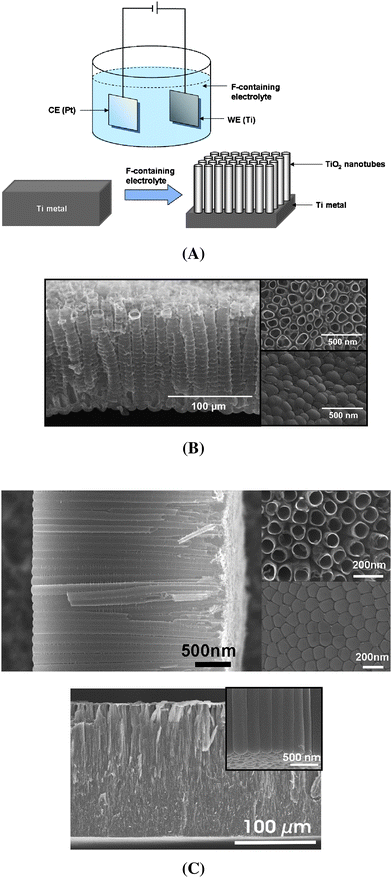 | ||
| Fig. 4 (A) Schematic diagram of a electrochemical set-up and anodic growth of TiO2 nanotubes on a Ti-metal sheet. (B) SEM images of the self-organized nanotubeTiO2 layer formed in aqueous electrolyte (1 M Na2SO4/0.14 M NaF electrolyte). (C) SEM images of TiO2 nanotube layers formed by the anodic oxidation of Ti-metal in non-aqueous electrolyte (cross section, top view and bottom view) and also showing a very high-aspect-ratio nanotube layer (several hundred μm). | ||
Nowadays, even more advanced geometries of TiO2 nanotubes can be prepared by altering the voltage during growth.15,85,86 For example, by regular voltage cycling a ‘bamboo-type’ morphology of TiO2 nanotubes can be grown in HF-containing ethylene glycol electrolyte15,85 (Fig. 5A). By using different AV pulse durations the distance between the ‘bamboo rings’ can be adjusted. Voltage stepping furthermore allows the growth of branched tubes (tube multilayers) or some 2D TiO2 networks (nanolaces).85,87–89
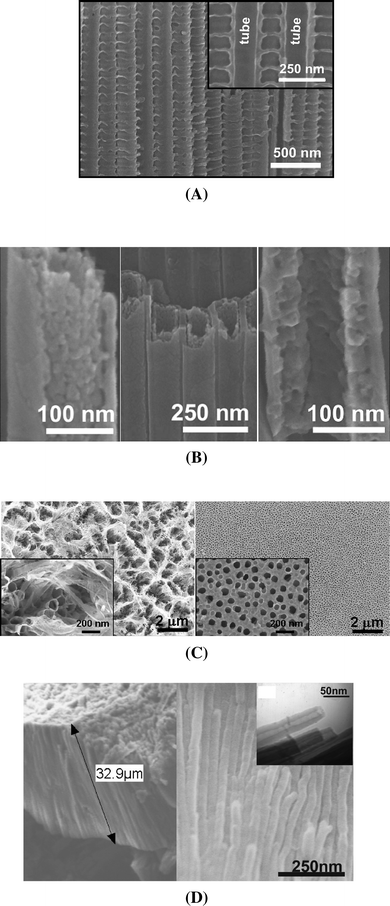 | ||
| Fig. 5 Example of advanced geometries of self-organized TiO2 nanotube layers: (A) A ‘bamboo-type’ nanotube layer (inset: half broken tube); (Reproduced with permission from ref. 85. Copyright Wiley-VCH, 2008). (B) Double-walled TiO2 nanotube structure; (Reproduced with permission from ref. 90. Copyright Wiley-VCH, 2008). (C) Nanograss formation at TiO2 tube tops under normal anodization conditions (left) and after pre-conditioning (Reproduced with permission from ref. 16. Copyright Elsevier, 2008). (D) 2nanotubes grown by rapid breakdown anodization; (Reproduced with permission from ref. 94. Copyright Elsevier, 2007). | ||
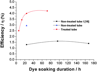
Recently we reported that adequate heat treatment of some TiO2 nanotubes leads to the characteristic double-wall structure shown in Fig. 5B.90 The smooth tubes are grown in ethylene glycol electrolytes and then, by rapid thermal annealing, the tubes are separated in two separate entities. As shown in Fig. 5B, the inner wall has a very high porosity providing a high surface area and the outer wall of the tubes is comparably smooth. A common feature is observed, if self-organized tubes are grown for extended periods of time: ‘grass’ formation at the tube top occurs. Although several times attributed to the formation of nanorods, nanospikes, or nanowires,91 this feature simply originates from the continuous thinning of the tube walls in the fluoride electrolyte. These ‘grassy’ tube tops may interfere with the defined electron transfer through nanotubes but in any case the disorder at the tube top may hamper optimized solar cell performance. In order to avoid this problem, various approaches have been developed to achieve ordered and open tube tops (Fig. 5C)15,18,92,93 and effects on the solar cell performance will be discussed in next section.
Another electrochemical approach to form high aspect nanotubes is so called rapid breakdown anodization (RBA).94–96 Such tubes form very rapidly (within seconds), if Ti is anodized under breakdown conditions in chloride or perchlorate containing electrolytes. This rapid process leads to formation of flower-like bundles of nanotubes as shown in Fig. 5D, with very high aspect ratio of tubes having lengths of 3–50 μm within some minutes. These structures have also been reported to show a good performance in DSSC.96,97
2.2. Modification and characterization of TiO2 nanotubes
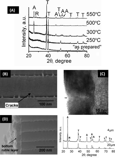 | ||
| Fig. 6 (A) XRD analysis of TiO2 nanotube layers at different annealing temperatures, revealing the amorphous ‘as-prepared’ material and anatase ‘A’ or rutile ‘R’ formation after the heat treatment. (B)–(C) SEM and TEM images of TiO2 nanotubes after annealing at 450 °C showing the crack lines and the grains present in the tube wall, respectively. (D) SEM image of TiO2 nanotubes after annealing at 450 °C showing the bottom rutile layer underneath the nanotubes. Inset: XRD of short tubes (4 μm) and long tubes (20 μm), indicating the rutile peak only for short tubes. | ||
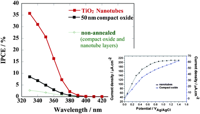 | ||
| Fig. 7 Photoelectrochemical behavior of TiO2 nanotubes and compact oxide layers on annealing (photocurrent spectra taken in 0.1M Na2SO4 at 500 mV vs. Ag/AgCl. Inset: voltage dependence of the photocurrent measured at a wavelength of 350 nm for the annealed samples). | ||
2.3 Tubes in DSSCs
For example, Kang and his group29 fabricated highly ordered TiO2 nanotubes using a nanoporous alumina templating method. Such nanotubes with 15 μm lengths were heat treated at 500 °C for 30 min and soaked in N3 dye for 24 h, which afterwards showed a solar cell efficiency of 3.5%. Some efforts are directed towards using completely anodized sputter-deposited layers on conductive glass117,120 but claims such as conversion efficiency of 2.9% fabricated on an only 360-nm-thick TiO2 nanotube arrays on conductive glass substrates remain unconfirmed and somewhat questionable.117 In particular, sputtering or evaporating a >10 μm thick Ti-metal layer on conductive glass to convert it to TiO2 nanotubes or lift-off processes seem not economically competitive. On the other hand, recent reports on hydrothermally fabricated nanorods such as the work by Liu et al.121 may provide valuable alternatives. Recently, Grätzel and his co-workers19 fabricated a flexible dye-sensitized solar cell from highly ordered TiO2 nanotube layers further treated with TiCl4. They used the conductive polymer Pt/ITO-PEN as the counter electrode in combination with an ionic liquid electrolyte. The solar cell performance depends on the thickness of the nanotube layers, and the highest energy conversion efficiency of 3.6% at AM 1.5 simulated full sunlight was obtained for 14 μm long tubes.
Also, RBA tubes (shown in Fig. 5D) were used in DSSCs (in a similar arrangement to Fig. 2B). The growth process leads to the advantage that high-aspect-ratio nanostructures (several dozens of μm in length vs. several dozens of nm in diameter) in the form of nanobundles can be prepared in a very short time (minutes). Some points regarding these tubes will be discussed in section 2.3.9.
The most detailed study on charge carrier behaviour in dye-sensitized TiO2 nanotube arrays stems from Jennings et al.14 It was shown that at about 20 μm tube length, IPCE values close to 100% could be obtained (Fig. 8A) when corrected for reflection losses. The measured and calculated IPCE values for 20 μm long nanotubes show good agreement. Most remarkable is that the electron diffusion length, based on experimental results to determine the diffusion coefficient and lifetime of the photoinjected electrons is of the order of 100 μm in the titania nanotube cells (Fig. 8B). This means a value of L that is significantly larger than 20 μm and 100% collection of electrons (without recombination) could be achieved with significantly longer tubes. The value of Lel = 100 μm seems to be in contrast to a value of Lel ≈ 30 μm obtained from data in the work by Zhu et al.18,25 However, it seems that tube properties are sensitive to the preparation procedure as mentioned in the next section, as for the differently prepared nanotubes considerable differences in Lel were obtained. The study of Jennings et al.14 also revealed a substantial discrepancy between the shapes of the electron trap distributions measured experimentally using charge extraction techniques and those inferred indirectly from transient current and voltage measurements.
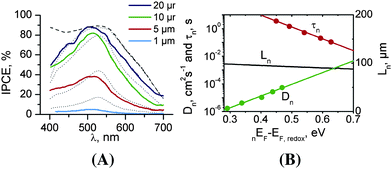 | ||
| Fig. 8 (A) Comparison of measured (solid line) and calculated (dotted line) IPCE values for different thicknesses of TiO2 nanotube layers; dashed line – the calculated IPCE spectrum for 20 μm long nanotubes without including the absorption loss due to I3 in the electrolyte. (B) Estimation of electron diffusion length (Ln) of 20 μm long TiO2 nanotubes from the experimental values of Dn and τc by taking the quasi Fermi level (QFL) into account. (Reproduced with permission from ref. 14. Copyright American Chemical Society, 2008). | ||
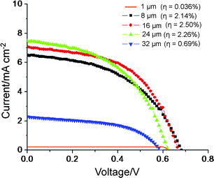 | ||
| Fig. 9 I–V characteristics measured for the solar cell configuration of Fig. 2B for different lengths of TiO2 nanotube layers after annealing at 450 °C for 1 h using commercial R50 as electrolyte and dye soaking (N719) for 1 day. | ||
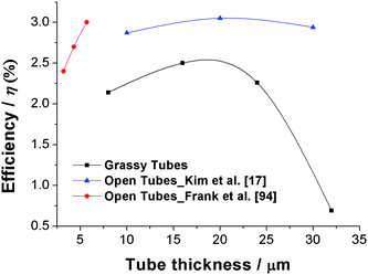
The tube diameter also has significant effect on the solar cell performance. It was found that for the same thickness of nanotube layers, smaller diameter tubes show a higher energy conversion efficiency.17Fig. 10 compiles a series of results obtained for several different tube geometries. Although some details such as the electrolyte or solar cell geometry vary slightly in different articles, the clear trend that a smaller diameter (at the same length) increases the solar cell response is observed as indicated in the inset. These findings overall correlate with the trend that an increase in the surface area of tubes increases the specific dye loading. This holds for decreasing the diameter or increasing the length of the nanotubes. In several cases this finding was confirmed by dye desorption measurements.14,17 As a bottom line for the tubes: though a better electrical performance is provided than in nanoparticulate layers, the lower specific surface area [BETtubes ≈ 30 m2 g−1; BETnanoparticles ≈ 80 m2 g−1] lowers the dye loading and thus reduces the efficiency. Some measures against this will be discussed in sections 2.3.5 and 2.3.8.
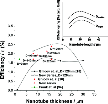 | ||
| Fig. 10 Influence of tube geometry: Comparison of solar cell efficiencies from literature and unpublished data, illustrating the effect of TiO2 nanotube length and diameter. All of the new series of experiments were carried out using R50 as electrolyte and N719 dye soaking for 1 day. Inset: Schematic trend of solar cell performances of TiO2 nanotube layers with tube length and diameter. | ||
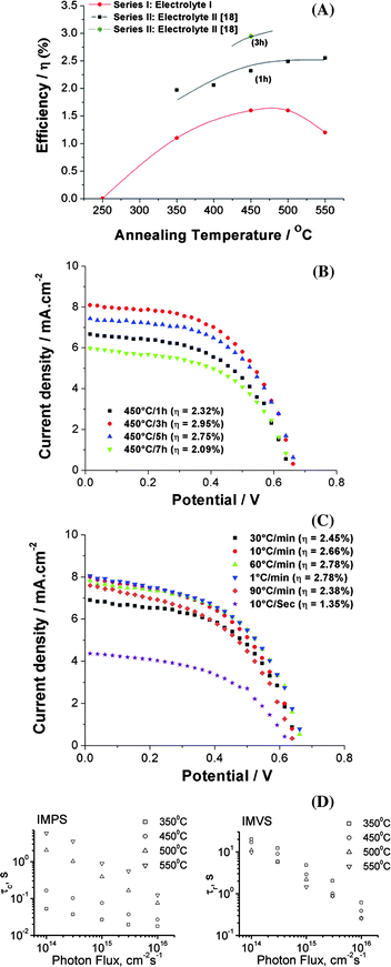 | ||
| Fig. 11 Influence of tube annealing: (A) Compilation of solar cell efficiencies of 16 μm TiO2 nanotube layers at different annealing temperatures (Series I measurements were carried out with 0.1 M lithium iodide +0.05 M iodine containing 0.6M tert-butyl pyridine as electrolyte I and Series II measurements were carried out using R50 as electrolyte II and N719 as dye for both cases). (B) I–V characteristics of 16 μm TiO2 nanotube layers annealed at 450 °C for different durations; (C) I–V characteristics of 16 μm TiO2 nanotube layers annealed at 450 °C for different annealing ramping speeds. (D) Electron transport (τc) and recombination time (τr) constants calculated from IMPS and IMVS curves for 16 μm TiO2 nanotube layer-based DSSCs at different annealing temperatures (reproduced with permission from ref. 17. Copyright Wiley-VCH, 2009). | ||
Very remarkable is a recent finding by Ghicov et al.17 that the electron transport properties through nanotubes can strongly depend on the annealing temperature. The electron recombination (τr) and transport time constants (τc) can be evaluated by intensity-modulated photocurrent spectroscopy (IMPS) and intensity-modulated photovoltage spectroscopy (IMVS) measurements as shown in Fig. 11D (from ref. 17). Extracting the transport time constants shows that τc is 10× smaller for tubes annealed at 350 °C compared with tubes annealed at 450 °C, which means the electron transport is drastically faster in the tubes annealed at 350 °C. This may be attributed to many fewer cracks induced at this annealing temperature100 or less rutile formation underneath the tubes. Although the finding of high rate constants at lower annealing temperatures is extremely promising for further research, the authors point out in their article that for these tubes a significantly lower dye loading was attained. The reasons for this at the current stage are unclear and further work is required to possibly exploit these effects.
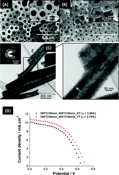 | ||
| Fig. 12 Influence of TiCl4 treatment: (A)–(B) SEM images of TiO2 nanotubes before and after TiCl4 treatment, showing tube decoration with TiO2 nanoparticles (reproduced with permission from ref. 129. Copyright Elsevier, 2009). (C) TEM and HRTEM of TiO2 nanotubes after TiCl4 treatment. (D) I–V curve for non-treated (NT) and treated tubes (TT). | ||
In order to avoid these problems, or at least reduce it, several approaches have been developed by various researchers. Frank and his co-workers25 improved the solar cell efficiency from 1.6% to 1.9% by modifying the cleaning and drying step using supercritical CO2 drying of tube layers. This approach leads to bundle-free and crack-free nanotube films. The positive effect on the solar cell efficiency was ascribed to an enhancement of the total surface area and making the tube tops more accessible to dye molecules. According to these authors, the inter-tube connection in the compact nanotube bundle effects the electron transport mechanism from the expected one-dimensional pathway to a mixture of one- and three-dimensional pathways. By making bundle-free and crack-free nanotubes, the one-dimensional transport shortens the transport pathway and reduces multiple electron trapping events.
Another approach to making ‘nanograss-free’ TiO2 nanotubes is by polishing the Ti-foil prior to anodization.16 A protective top layer can be formed on polished Ti samples, which delays the chemical attack of the tube ends and thus the formation of ‘nanograss’ and tube bundling can be avoided. Additionally, the layer seems also to act as a stratification against disorder induced by the drying process. Such highly aligned, ordered, and ‘nanograss’-free geometries show higher solar cell efficiencies than the conventional nanotubes (see Fig. 14). The maximum energy conversion efficiency is obtained again for 20 μm thick nanotube layers. The open-circuit voltage of nanograss-free nanotubes is found to be higher than that for ‘grassy’ tubes. This may be due to the fact that in more ordered grass-free tubes the electron lifetime is higher due to the presence of fewer defects.
 | ||
| Fig. 14 Influence of tube top morphology: A comparative study of solar cell performances of ‘nanograss-free’ and ‘grassy’ tube tops of TiO2 layers. | ||
Another approach to create top ordered layer was reported by Song et al.93 In this approach a thermal rutile layer is first formed on the Ti metal surface and tubes are then grown underneath. This treatment was found to be very effective to produce defined tubetops up to considerable length of >50 μm.93 Clearly, such tubes are very promising in view of achieving defined tube tops. Most recently also direct growth approaches in optimized electrolytes are being explored to avoid “grass” formation.92 However, it should be noted that smooth and regular tube tops may not represent the most ideal case as the disorder has an anti-reflection effect which helps high light harvesting as evident from the high Isc values.
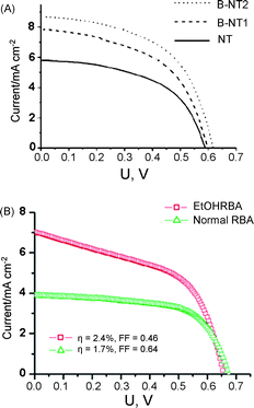 | ||
| Fig. 15 Influence of tube morphology modifications: I–V characteristics for DSSCs of different advanced geometries of TiO2 nanotubes. (A) Bamboo nanotube (B-NT) with different ring distance and normal nanotubes (NT) (reproduced with permission from ref. 15. Copyright American Chemical Society, 2008). (B) RBA tubes formed in aqueous electrolyte and in ethanolic electrolyte. | ||
2.4 Conclusions
The present article tries to give an overview of the current state of using TiO2 nanotubes in DSSCs. It is remarkable that since the first results in 2005 with efficiencies of 0.04%, reproducible results in the order of 4–5% efficiency have since been obtained. This although a number of parameters, such as, tube annealing, dye optimization and solar cell geometry, are far from optimized. Exciting results involve the finding of much higher electron diffusion length in tubes than in particles, and the finding that the tube geometry strongly affects electron lifetime – in optimized tubes electron diffusion lengths of ∼100 μm have been observed. The fact that annealing conditions strongly affect electron collection values give room for significant improvement as here one of the crucial loss mechanisms in DSSCs (recombination with the electrolyte) can be reduced. While some higher efficiencies up to 7% have been reported in literature for mixing tubes with nanoparticles, one has to carefully judge if these effects are indeed due to tubes or must be ascribed primarily to the effect of the nanoparticles.However, from the current state of investigations it is clear that specific dye loading in the tubes need to be improved – i.e., TiO2 structures with a larger surface area need to be created. This may be achieved in various ways by modifying the tube walls with porous materials (double-walled tubes), TiO2 nanoparticle decoration or creating defined ‘bamboo-type’ rings. Also, several issues relating to practical solar cell construction, such as, front- or backside illumination, optimized layout, surface reflectivity, or designed light absorption are further open research areas and exciting new findings can also be expected in the development in these “technology” areas.
References
- F. Pfisterer, Photovoltaic Cells, Ullmann's Encyclopedia of Industrial Chemistry, 2002,Wiley-VCH, Germany Search PubMed.
- J. Desilvestro, M. Grätzel, L. Kavan and J. Moser, J. Am. Chem. Soc., 1985, 107, 2988 CrossRef CAS.
- N. Vlachopoulos, P. Liska, J. Augustynski and M. Grätzel, J. Am. Chem. Soc., 1988, 110, 1216 CrossRef CAS.
- B. O'Regan and M. Grätzel, Nature, 1991, 353, 737 CrossRef CAS.
- M. Grätzel, Nature, 2001, 414, 338 CrossRef CAS.
- M. K. Nazeeruddin, F. D. Angelis, S. Fantacci, A. Selloni, G. Viscardi, P. Liska, S. Ito, B. Takeru and M. Grätzel, J. Am. Chem. Soc., 2005, 127, 16835 CrossRef CAS.
- Y. Chiba, A. Islam, Y. Watanabe, R. Komiya, N. Koide and L. Han, Jpn. J. Appl. Phys., 2006, 45, L638 CrossRef CAS.
- M. Grätzel, Inorg. Chem., 2005, 44, 6841 CrossRef.
- S. E. Koops, B. C. O'Regan, P. R. F. Barnes and J. R. Durrant, J. Am. Chem. Soc., 2009, 131, 4808 CrossRef CAS.
- J. Nelson, Phys. Rev. B: Condens. Matter Mater. Phys., 1999, 59, 15374 CrossRef CAS LP.
- J. Bisquert, Phys. Rev. Lett., 2003, 91, 010602 CrossRef.
- S. Nakade, Y. Saito, W. Kubo, T. Kitamura, Y. Wada and S. Yanagida, J. Phys. Chem. B, 2003, 107, 8607 CrossRef CAS.
- L. M. Peter, J. Phys. Chem. C, 2007, 111, 6601 CrossRef CAS.
- J. R. Jennings, A. Ghicov, L. M. Peter, P. Schmuki and A. B. Walker, J. Am. Chem. Soc., 2008, 130, 13364 CrossRef CAS.
- D. Kim, A. Ghicov, S. P. Albu and P. Schmuki, J. Am. Chem. Soc., 2008, 130, 16454 CrossRef CAS.
- D. Kim, A. Ghicov and P. Schmuki, Electrochem. Commun., 2008, 10, 1835 CrossRef CAS.
- A. Ghicov, S. Albu, R. Hahn, D. Kim, T. Stergiopoulos, J. Kunze, C.-A. Schiller, P. Falaras and P. Schmuki, Chem.–Asian J., 2009, 4, 520 CrossRef.
- K. Zhu, N. R. Neale, A. Miedaner and A. J. Frank, Nano Lett., 2007, 7, 69 CrossRef CAS.
- D. Kuang, J. Brillet, P. Chen, M. Takata, S. Uchida, H. Miura, K. Sumioka, S. M. Zakeeruddin and M. Grätzel, ACS Nano, 2008, 2, 1113 CrossRef CAS.
- S. H. Kang, S.-H. Choi, M.-S. Kang, J.-Y. Kim, H.-S. Kim, T. Hyeon and Y.-E. Sung, Adv. Mater., 2008, 20, 54 CrossRef CAS.
- M. Y. Song, D. K. Kim, K. J. Ihn, S. M. Jo and D. Y. Kim, Nanotechnology, 2004, 15, 1861 CrossRef CAS.
- S. Pavasupree, S. Ngamsinlapasathian, Y. Suzuki and S. Yoshikawa, J. Nanosci. Nanotechnol., 2006, 6, 3685 CrossRef CAS.
- Y. Ohsaki, N. Masaki, T. Kitamura, Y. Wada, T. Okamoto, T. Sekino, K. Niihara and S. Yanagida, Phys. Chem. Chem. Phys., 2005, 7, 4157 RSC.
- M. Adachi, Y. Murata, J. Takao, J. Jiu, M. Sakamoto and F. Wang, J. Am. Chem. Soc., 2004, 126, 14943 CrossRef CAS.
- K. Zhu, T. B. Vinzant, N. R. Neale and A. J. Frank, Nano Lett., 2007, 7, 3739 CrossRef CAS.
- H.-H. Ou and S.-L. Lo, Sep. Purif. Technol., 2007, 58, 179 CrossRef CAS.
- X. Chen and S. S. Mao, Chem. Rev., 2007, 107, 2891 CrossRef CAS.
- D. V. Bavykin, J. M. Friedrich and F. C. Walsh, Adv. Mater., 2006, 18, 2807 CrossRef CAS.
- T.-S. Kang, A. P. Smith, B. E. Taylor and M. F. Durstock, Nano Lett., 2009, 9, 601 CrossRef CAS.
- G. R. Patzke, F. Krumeich and R. Nesper, Angew. Chem., Int. Ed., 2002, 41, 2446 CrossRef.
- A. Ghicov and P. Schmuki, Chem. Commun., 2009, 2791 RSC.
- J. M. Macak, H. Tsuchiya, A. Ghicov, K. Yasuda, R. Hahn, S. Bauer and P. Schmuki, Curr. Opin. Solid State Mater. Sci., 2007, 11, 3 CrossRef CAS.
- M. J. Cass, A. B. Walker, D. Martinez and L. M. Peter, J. Phys. Chem. B, 2005, 109, 5100 CrossRef CAS.
- N. G. Park, J. van de Lagemaat and A. J. Frank, J. Phys. Chem. B, 2000, 104, 8989 CrossRef CAS.
- H. Lindström, A. Holmberg, E. Magnusson, S. E. Lindquist, L. Malmqvist and A. Hagfeldt, Nano Lett., 2001, 1, 97 CrossRef.
- H. Lindström, E. Magnusson, A. Holmberg, S. Sodergren, S. E. Lindquist and A. Hagfeldt, Sol. Energy Mater. Sol. Cells, 2002, 73, 91 CrossRef.
- A. Mishra, M. K. R. Fischer and P. Bauerle, Angew. Chem., Int. Ed., 2009, 48, 2474 CrossRef CAS.
- N. Robertson, Angew. Chem., Int. Ed., 2006, 45, 2338 CrossRef CAS.
- M. Grätzel, Progr. Photovolt.: Res. Appl., 2006, 14, 429 Search PubMed.
- M. Grätzel, J. Photochem. Photobiol., A, 2004, 164, 3 CrossRef CAS.
- P. Bonhôte, A.-P. Dias, N. Papageorgiou, K. Kalyanasundaram and M. Grätzel, Inorg. Chem., 1996, 35, 1168 CrossRef CAS.
- S. Hwang, J. H. Lee, C. Park, H. Lee, C. Kim, C. Park, M.-H. Lee, W. Lee, J. Park, K. Kim, N.-G. Park and C. Kim, Chem. Commun., 2007, 4887 RSC.
- M. K. Nazeeruddin, A. Kay, I. Rodicio, R. Humpbry-Baker, E. Miiller, P. Liska, N. Vlachopoulos and M. Grätzel, J. Am. Chem. Soc., 1993, 115, 6382 CrossRef CAS.
- M. K. Nazeeruddin, P. Pechy and M. Grätzel, Chem. Commun., 1997, 1705 RSC.
- M. K. Nazeeruddin, S. M. Zakeeruddin, R. Humphrey-Baker, M. Jirousek, P. Liska, N. Vlachopoulos, V. Shklover, C.-H. Fischer and M. Grätzel, Inorg. Chem., 1999, 38, 6298 CrossRef CAS.
- D. Kuciauskas, M. S. Freund, H. B. Gray, J. R. Winkler and N. S. Lewis, J. Phys. Chem. B, 2001, 105, 392 CrossRef CAS.
- R. Argazzi, G. Larramona, C. Contado and C. A. Bignozzi, J. Photochem. Photobiol., A, 2004, 164, 15 CrossRef CAS.
- A. Islam, H. Sugihara, K. Hara, L. P. Singh, R. Katoh, M. Yanagida, Y. Takahashi, S. Murata and H. Arakawa, Inorg. Chem., 2001, 40, 5371 CrossRef CAS.
- E. A. M. Geary, L. J. Yellowlees, L. A. Jack, I. D. H. Oswald, S. Parsons, N. Hirata, J. R. Durrant and N. Robertson, Inorg. Chem., 2005, 44, 242 CrossRef CAS.
- N. Alonso-Vante, J.-F. Nierengarten and J.-P. Sauvage, J. Chem. Soc., Dalton Trans., 1994, 1649 RSC.
- P. M. Jayaweera, S. S. Palayangoda and K. Tennakone, J. Photochem. Photobiol., A, 2001, 140, 173 CrossRef CAS.
- P. Wang, C. Klein, J.-E. Moser, R. Humphry-Baker, N.-L. Cevey-Ha, R. Charvet, P. Comte, S. M. Zakeeruddin and M. Grätzel, J. Phys. Chem. B, 2004, 108, 17553 CrossRef CAS.
- H. Park, E. Bae, J.-J. Lee, J. Park and W. Choi, J. Phys. Chem. B, 2006, 110, 8740 CrossRef CAS.
- K. Hara, Z.-S. Wang, T. Sato, A. Furube, R. Katoh, H. Sugihara, Y. Dan-oh, C. Kasada, A. Shinpo and S. Suga, J. Phys. Chem. B, 2005, 109, 15476 CrossRef CAS.
- S. Alex, U. Santhosh and S. Das, J. Photochem. Photobiol., A, 2005, 172, 63 CrossRef CAS.
- T. Horiuchi, H. Miura, K. Sumioka and S. Uchida, J. Am. Chem. Soc., 2004, 126, 12218 CrossRef CAS.
- W. M. Campbell, A. K. Burrell, D. L. Officer and K. W. Jolley, Coord. Chem. Rev., 2004, 248, 1363 CrossRef CAS.
- Q. Wang, W. M. Campbell, E. E. Bonfantani, K. W. Jolley, D. L. Officer, P. J. Walsh, K. Gordon, R. Humphrey-Baker, M. K. Nazeeruddin and M. Grätzel, J. Phys. Chem. B, 2005, 109, 15397 CrossRef CAS.
- M. Grätzel, J. Photochem. Photobiol., C, 2003, 4, 145 CrossRef CAS.
- Z.-S. Wang, K. Sayama and H. Sugihara, J. Phys. Chem. B, 2005, 109, 22449 CrossRef CAS.
- H. Nusbaumer, J.-E. Moser, S. M. Zakeeruddin, M. K. Nazeeruddin and M. Grätzel, J. Phys. Chem. B, 2001, 105, 10461 CrossRef CAS.
- S. A. Sapp, C. M. Elliott, C. Contado, S. Caramori and C. A. Bignozzi, J. Am. Chem. Soc., 2002, 124, 11215 CrossRef CAS.
- G. Oskam, B. V. Bergeron, G. J. Meyer and P. C. Searson, J. Phys. Chem. B, 2001, 105, 6867 CrossRef CAS.
- P. Wang, S. M. Zakeeruddin, J.-E. Moser, R. Humphry-Baker and M. Grätzel, J. Am. Chem. Soc., 2004, 126, 7164 CrossRef CAS.
- G. Boschloo, L. Haggman and A. Hagfeldt, J. Phys. Chem. B, 2006, 110, 13144 CrossRef CAS.
- D. B. Kuang, C. Klein, Z. P. Zhang, S. Ito, J. E. Moser, S. M. Zakeeruddin and M. Grätzel, Small, 2007, 3, 2094 CrossRef CAS.
- J.-H. Yum, P. Chen, M. Grätzel and M. K. Nazeeruddin, Chem. Sus. Chem., 2008, 1, 699 CrossRef CAS.
- H. J. Snaith and L. Schmidt-Mende, Adv. Mater., 2007, 19, 3187 CrossRef CAS.
- Y. Bai, Y. Cao, J. Zhang, M. Wang, R. Li, P. Wang, S. M. Zakeeruddin and M. Grätzel, Nat. Mater., 2008, 7, 626 CrossRef CAS.
- A. B. F. Martinson, J. W. Elam, J. T. Hupp and M. J. Pellin, Nano Lett., 2007, 7, 2183 CrossRef CAS.
- N. N. Dinh, M.-C. Bernard, A. H.-L. Goff, T. Stergiopoulos and P. Falaras, C. R. Chim., 2006, 9, 676 CrossRef CAS.
- K. Tennakone, G. R. R. Kumara, I. R. M. Kottegoda and V. S. P. Perera, Chem. Commun., 1999, 15 RSC.
- K. Sayama, H. Suguhara and H. Arakawa, Chem. Mater., 1998, 10, 3825 CrossRef CAS.
- F. Lenzmann, J. Krueger, S. Burnside, K. Brooks, M. Grätzel, D. Gal, S. Rühle and D. Cahen, J. Phys. Chem. B, 2001, 105, 6347 CrossRef CAS.
- J. B. Baxter and E. S. Aydil, Appl. Phys. Lett., 2005, 86, 053114 CrossRef.
- P. Schmuki, in Electrochemistry at the Nanoscale, ed. P. Schmuki and S. Virtanen, Springer, New York, 1st edn, 2009, pp. 435–466 Search PubMed.
- V. Zwilling, E. Darque-Ceretti, A. Boutry-Forveille, D. David, M. Y. Perrin and M. Aucouturier, Surf. Interface Anal., 1999, 27, 629 CrossRef CAS.
- D. Gong, C. A. Grimes, O. K. Varghese, Z. Chen and E. C. Dickey, J. Mater. Res., 2001, 16, 3331 CrossRef CAS.
- R. Beranek, H. Hildebrand and P. Schmuki, Electrochem. Solid-State Lett., 2003, 6, B12 CrossRef CAS.
- J. M. Macak, K. Sirotna and P. Schmuki, Electrochim. Acta, 2005, 50, 3679 CrossRef CAS.
- J. M. Macak, H. Tsuchiya, L. Taveira, S. Aldabergerova and P. Schmuki, Angew. Chem., Int. Ed., 2005, 44, 7463 CrossRef CAS.
- J. M. Macák, H. Tsuchiya and P. Schmuki, Angew. Chem., Int. Ed., 2005, 44, 2100 CrossRef CAS.
- S. P. Albu, A. Ghicov, J. M. Macak and P. Schmuki, Phys. Status Solidi RRL, 2007, 1, R65 Search PubMed.
- J. M. Macak, S. P. Albu and P. Schmuki, Phys. Status Solidi RRL, 2007, 1, 181 Search PubMed.
- S. P. Albu, D. Kim and P. Schmuki, Angew. Chem., Int. Ed., 2008, 47, 1916 CrossRef CAS.
- W. Chanmanee, A. Watcharenwong, C. R. Chenthamarakshan, P. Kajitvichyanukul, N. R. Tacconi and K. Rajeshwar, J. Am. Chem. Soc., 2008, 130, 965 CrossRef CAS.
- Y.-Y. Song, F. Schmidt-Stein, S. Bauer and P. Schmuki, J. Am. Chem. Soc., 2009, 131, 4230 CrossRef CAS.
- J. M. Macak, S. Albu, D. H. Kim, I. Paramasivam, S. Aldabergerova and P. Schmuki, Electrochem. Solid-State Lett., 2007, 10, K28 CrossRef CAS.
- K. Yasuda and P. Schmuki, Electrochem. Commun., 2007, 9, 615 CrossRef CAS.
- S. P. Albu, A. Ghicov, S. Aldabergenova, P. Drechsel, D. LeClere, G. E. Thompson, J. M. Macak and P. Schmuki, Adv. Mater., 2008, 20, 4135 CAS.
- J. H. Lim and J. Choi, Small, 2007, 3, 1504 CrossRef CAS.
- K. Lee, D. Kim, P. Roy and P. Schmuki, unpublished work.
- Y.-Y. Song, R. Lynch, D. Kim, P. Roy and P. Schmuki, Electrochem. Solid-State Lett., 2009, 12, C17 CrossRef CAS.
- R. Hahn, J. M. Macak and P. Schmuki, Electrochem. Commun., 2007, 9, 947 CrossRef CAS.
- K. Nakayama in: 208th ECS Meeting, California, 2005, abstract 819 and abstract 843 Search PubMed.
- K. Ishibashi, R. Yamaguchi, Y. Kimura and M. Niwano, J. Electrochem. Soc., 2008, 155, K10 CrossRef CAS.
- R. Hahn, T. Stergiopoulus, J. M. Macak, D. Tsoukleris, A. G. Kontos, S. P. Albu, D. Kim, A. Ghicov, J. Kunze, P. Falaras and P. Schmuki, Phys. Status Solidi RRL, 2007, 1, 135 Search PubMed.
- H. Tang, K. Prasad, R. Sanjinbs, P. E. Schmid and F. Levy, J. Appl. Phys., 1994, 75, 2042 CrossRef CAS.
- N.-G. Park, J. van de Lagemaat and A. J. Frank, J. Phys. Chem. B, 2000, 104, 8989 CrossRef CAS.
- S. P. Albu, H. Tsuchiya, S. Fujimoto and P. Schmuki, Chem. Phys. Lett., 2009 Search PubMed , to be submitted.
- R. P. Vitiello, J. M. Macak, A. Ghicov, H. Tsuchiya, L. F. P. Dick and P. Schmuki, Electrochem. Commun., 2006, 8, 544 CrossRef CAS.
- J. M. Macak, A. Ghicov, R. Hahn, H. Tsuchiya and P. Schmuki, J. Mater. Res., 2006, 21, 2824 CrossRef CAS.
- R. Hahn, A. Ghicov, J. Salonen, V.-P. Lehto and P. Schmuki, Nanotechnology, 2007, 18, 105604 CrossRef.
- R. Hahn, F. Schmidt-Stein, J. Salonen, S. Thiemann, Y. Y. Song, J. Kunze, V.-L. Lehto and Patrik Schmuki, Angew. Chem., Int. Ed., 2009, 48, 7236 CrossRef CAS.
- R. Beranek, H. Tsuchiya, T. Sugishima, J. M. Macak, L. Taveira, S. Fujimoto, H. Kisch and P. Schmuki, Appl. Phys. Lett., 2005, 87, 243114 CrossRef.
- W. W. Gärtner, Phys. Rev., 1959, 116, 84 CrossRef CAS.
- J. W. Schultze and M. M. Lohrengel, Electrochim. Acta, 2000, 45, 2499 CrossRef CAS.
- L. V. Taveira, A. A. Sagües, J. M. Macak and P. Schmuki, J. Electrochem. Soc., 2008, 155, C293 CrossRef CAS.
- H. Tsuchiya, J. M. Macak, A. Ghicov, A. S. Räder, L. Taveira and P. Schmuki, Corros. Sci., 2007, 49, 203 CrossRef CAS.
- U. Diebold, Surf. Sci. Rep., 2003, 48, 53 CrossRef CAS.
- A. Hagfeldt, U. Björksten and M. Gra1tzel, J. Phys. Chem., 1996, 100, 8045 CrossRef CAS.
- S. Södergren, A. Hagfeldt, J. Olsson and S.-E. Lindquist, J. Phys. Chem., 1994, 98, 5552 CrossRef.
- R. Lynch, A. Ghicov and P. Schmuki, J. Electrochem. Soc., submitted Search PubMed.
- J. M. Macak, H. Tsuchiya, A. Ghicov and P. Schmuki, Electrochem. Commun., 2005, 7, 1133 CrossRef CAS.
- T. Stergiopoulos, A. Ghicov, V. Likodimos, D. S. Tsoukleris, J. Kunze, P. Schmuki and P. Falaras, Nanotechnology, 2008, 19, 235602 CrossRef.
- K.-M. Lee, V. Suryanarayanan, J.-H. Huang, K. R. J. Thomas, J. T. Lin and K.-C. Ho, Electrochim. Acta, 2009, 54, 4123 CrossRef CAS.
- G. K. Mor, K. Shankar, M. Paulose, O. K. Varghese and C. A. Grimes, Nano Lett., 2006, 6, 215 CrossRef CAS.
- J. H. Park, T.-W. Lee and M. G. Kang, Chem. Commun., 2008, 2867 RSC.
- W. J. Lee, E. Ramasamy and D. Y. Lee, Sol. Energy Mater. Sol. Cells, 2009, 93, 1448 CrossRef CAS.
- S. Berger, A. Ghicov, Y.-C. Nah and P. Schmuki, Langmuir, 2009, 25, 4841 CrossRef CAS.
- B. Liu, E. S. Aydil and J. Am, J. Am. Chem. Soc., 2009, 131, 3985 CrossRef CAS.
- V. Yong, S.-T. Ho and R. P. H. Chang, Appl. Phys. Lett., 2008, 92, 143506 CrossRef.
- J. Nelson, The Physics of Solar Cells, Imperial College Press, London, 2003, ch. 1 Search PubMed.
- L. Kavan, B. O'Regan, A. Kay and M. Grätzel, J. Electroanal. Chem., 1993, 346, 291 CrossRef CAS.
- M. K. Nazeeruddin, A. Kay, I. Rodicio, R. Humpbry-Baker, E. Miiller, P. Liska, N. Vlachopoulos and M. Grätzel, J. Am. Chem. Soc., 1993, 115, 6382 CrossRef CAS.
- N.-G. Park, G. Schlichthrl, J. van de Lagemaat, H. M. Cheong, A. Mascarenhas and A. J. Frank, J. Phys. Chem. B, 1999, 103, 3308 CrossRef CAS.
- S. Ito, P. Liska, P. Comte, R. Charvet, P. Pechy, U. Bach, L. Schmidt-Mende, S. M. Zakeeruddin, A. Kay, M. K. Nazeeruddin and M. Grätzel, Chem. Commun., 2005, 4351 RSC.
- B. C. O'Regan, J. R. Durrant, P. M. Sommeling and N. J. Bakker, J. Phys. Chem. C, 2007, 111, 14001 CrossRef CAS.
- P. Roy, D. Kim, I. Paramasivam and P. Schmuki, Electrochem. Commun., 2009, 11, 1001 CrossRef CAS.
- P. Roy, D. Kim, K. Lee, E. Spiecker and P. Schmuki, unpublished work.
- S. Funk, B. Hokkanen, U. Burghaus, A. Ghicov and P. Schmuki, Nano Lett., 2007, 7, 1091 CrossRef CAS.
- D. Kim, J. M. Macak, F. Schimidt-Stein and P. Schmuki, Nanotechnology, 2008, 19, 305710 CrossRef.
| This journal is © The Royal Society of Chemistry 2010 |