GaOOH, and β- and γ-Ga2O3 nanowires: preparation and photoluminescence
Chih-Chia
Huang
and
Chen-Sheng
Yeh
*
Department of Chemistry, National Cheng Kung University, Tainan, Taiwan. E-mail: csyeh@mail.ncku.edu.tw
First published on 16th October 2009
Abstract
A composite methodology using laser ablation followed by a solution refluxing process was demonstrated to prepare GaOOH and (β-, γ-) Ga2O3 nanowires, where GaOOH and γ-Ga2O3 nanowires were prepared for the first time. The CTAB surfactant and PVP polymer facilitated the nucleation and growth of GaOOH nanorods, and played different roles in selectively controlling the growth rates of different facets. In the PVA/CTAB-assisted reaction, a high aspect ratio (of at least 200) of GaOOH nanowires was approached. The calcination of GaOOH nanowires at a temperature of 500 °C (6 h) transformed them into γ-Ga2O3 nanowires and converted them further into β-Ga2O3 nanowires at 750 °C (18 h). Photoluminescence measurements were conducted at room temperature for the GaOOH and (β-, γ-) Ga2O3 nanowires using a high resolution synchrotron X-ray source. The blue emissions from the GaOOH and (β-, γ-) Ga2O3 nanowires were resolved into a few sharp peaks, and may provide a valuable reference for further understanding the PL mechanisms. Although luminescence spectra of the GaOOH and γ-Ga2O3 nanowires were recorded for the first time, the similar optical band gap and emission contour observed for β-Ga2O3 nanowires suggests that the optical behavior of GaOOH and γ-Ga2O3 nanowires are likely to closely follow the PL mechanisms of β-Ga2O3 nanowires.
Introduction
Gallium oxide hydroxide (GaOOH) is considered to be an important precursor for the direct preparation of wide band-gap gallium oxide (Ga2O3), 4.2–4.9 eV,1,2 and gallium nitride (GaN), ∼3.4 eV,3 semiconductors by simple thermal transformation methods. In considering the polymorphism of Ga2O3, GaOOH could be transformed by dehydration into different phases of Ga2O3: α-, γ-, δ-, ε- and β-Ga2O3.4,5 β-Ga2O3 is a transparent conducting oxide and shows field emission characteristics in optoelectronics.6 α-, β- and γ-Ga2O3 have also been reported to have potential applications in the adsorption of chemical reagents (H2O, alcohols, carboxylic acids, CO and CO2).7–9One-dimensional (1D) nanomaterials have been the subject of intensive research due to their distinctive electronic, optoelectronic and mechanical properties.10–12 Considerable effort has been devoted to developing the bulk synthesis of 1D materials. Up to now, a number of wet chemistry approaches, such as forced hydrolysis,13 sol–gel methods,14 a protein filament templated approach,15 hydrothermal treatments16–18 and sonochemical processes19 have been employed to fabricate shaped GaOOH with a variety of morphologies, including rod-like,20–22 spindle-like5 and scroll-like cylindrical structures.19 However, the fabrication of GaOOH and γ-Ga2O3 nanowires remains a challenge, and has yet to be reported. In this study, GaOOH nanowires were synthesized and transformed into (β-, γ-) Ga2O3 nanowires by a thermal treatment.
Herein, we report that a composite strategy using laser ablation23 followed by a soft solution-phase approach24,25 at a low temperature of ∼121 °C has been developed to manipulate GaOOH nanorods and nanowires with a prism-like morphology. Two stabilizing agents, a polymer (PVP or PVA) and/or CTAB, were utilized to facilitate nanorod and nanowire formation, and had a cooperative effect on shape and size control. In the presence of PVA and CTAB, high aspect ratios (at least 200) of GaOOH nanowires were obtained. Following a calcination treatment, as-prepared GaOOH nanowires could readily form cubic γ-Ga2O3 (500 °C) and monoclinic β-Ga2O3 (750 °C) nanowires. The optical properties of the as-grown GaOOH and (β-, γ-) Ga2O3 nanowires were also investigated. The photoluminescence (PL) properties of the GaOOH and (β-, γ-) Ga2O3 nanowires were well resolved into a few sharp peaks using a high-resolution synchrotron X-ray source. As compared to the previous studies of β-Ga2O3 nanorods and nanowires, having a broad band emission covering from the UV to the visible region,1,2,5,16,17,26–28 our findings may provide a valuable reference for further understanding PL mechanisms.
Experimental
Preparation of GaOOH nanorods and nanowires
Laser ablation was performed by placing a gallium plate (>99.9%, 1.5 × 1 cm) on the bottom of a Pyrex vial filled with 5 mL of solution.23,24 The formation of GaOOH nanorods was achieved by the preparation of a 5 mL solution from a 4 mL aqueous solution containing 2.2 mmol of cetyltrimethylammonium bromide (CTAB) mixed with 1 mL of 2-propanol containing 1 mmol of poly(vinylpyrrolidone) (PVP, Mw = 40![[thin space (1/6-em)]](https://www.rsc.org/images/entities/char_2009.gif) 000). An unfocused Nd:YAG laser (Quantel Brilliant) operating at 10 Hz (5 ns pulse width) with a wavelength of 1064 nm was utilized to irradiate the Ga plate immersed in 5 mL of the as-prepared solution. In general, a laser intensity of 100 mJ pulse−1 was employed to ablate the metal plate with irradiation for a duration of 20 min. All manipulations were carried out in air. On the other hand, GaOOH nanowires were synthesized by the addition of 1 mL of 2-propanol containing 1 mmol of poly(vinylalcohol) (PVA; Mw = 22000) to a 4 mL aqueous solution containing 2.2 mmol of CTAB.
000). An unfocused Nd:YAG laser (Quantel Brilliant) operating at 10 Hz (5 ns pulse width) with a wavelength of 1064 nm was utilized to irradiate the Ga plate immersed in 5 mL of the as-prepared solution. In general, a laser intensity of 100 mJ pulse−1 was employed to ablate the metal plate with irradiation for a duration of 20 min. All manipulations were carried out in air. On the other hand, GaOOH nanowires were synthesized by the addition of 1 mL of 2-propanol containing 1 mmol of poly(vinylalcohol) (PVA; Mw = 22000) to a 4 mL aqueous solution containing 2.2 mmol of CTAB.
Once laser irradiation was complete, the resulting solutions were transferred into a round-bottomed flask for the refluxing process, and the solutions heated to ∼121 °C. A period of 23 h reflux led to the formation of GaOOH nanorods in the presence of PVP and GaOOH nanowires with lengths up to several tens of micrometers via PVA assistance. After completion of the reflux process, the solutions were allowed to cool to room temperature. The precipitates were collected and washed several times with distilled water to remove excess surfactants, and then dried in a vacuum desiccator. Calcination processes were performed to thermally treat the GaOOH nanowires at 500 °C for 6 h and at 750 °C for 18 h to obtain γ-Ga2O3 and β-Ga2O3 nanowires, respectively, under ambient pressure.
Characterization
Electron micrographs using transmission electron microscopes (TEM; JEOL 3010 at 300 kV and Philips CM-200 at 200 kV) were obtained by placing a drop of the sample on a copper mesh coated with an amorphous carbon film, followed by evaporation of the solvent in a vacuum desiccator. Scanning electron microscope (SEM) images accompanied by an energy dispersive spectrometer (EDS) analysis on Al substrates were carried out by using a Hitachi S4200 field emission SEM. X-Ray diffraction (XRD) data were collected on a Rigaku D-Max IIIV diffractometer using Cu-Kα radiation (λ = 1.54056 Å) at 30 kV and 30 mA. The optical properties of the GaOOH and (β-, γ-) Ga2O3 nanowires dispersed in an aqueous solution were monitored using a UV-vis spectrophotometer (Hewlett-Packard 8452A).Luminescence spectra were measured by a PL end station using synchrotron as the excitation radiation. In brief, VUV–UV light produced by the National Synchrotron Radiation Research Center in Taiwan was dispersed by a high-flux cylindrical grating monochromator (CGM; focal length 6 m) beam line. A focused and monochromatic beam was monitored with light reflected from an LiF beam splitter placed before the sample and at an angle of 45° to the beam line. The intensity of light reflected from the beam splitter defined the flux of the incident beam for normalization. Light transmitted through the LiF beam splitter irradiated the sample. The PL spectra of GaOOH and Ga2O3 anisotropic nanostructures were analyzed by a monochromator (Jobin-Yvon HR320, focal length 0.32 m) with a grating (1200 grooves mm−1) blazed at 500 nm. The fluorescence intensity of the sample was detected by a photomultiplier (Hamamatsu R943-02) in a photon-counting mode.
Results and discussion
Laser ablation was conducted in aqueous solutions containing CTAB and PVP. After laser irradiation for 20 min, the nascent solutions appeared transparent with a yellowish color.23,24 Subsequently, the nascent laser-ablated solutions were transferred to a round-bottomed flask for the reflux process, leading to a turbid whiteness. Fig. 1 displays TEM and SEM images of the GaOOH nanorods with lengths of up to 1.2–1.3 μm and an aspect ratio close to 7. The magnified SEM image shown in the inset of Fig. 1(b) reveals that these nanorods have a prism-like cross-section and that their lateral dimensions vary from 140 to 220 nm. These prismatic shapes are composed of an interior angle of 129.9° between two {110} surfaces.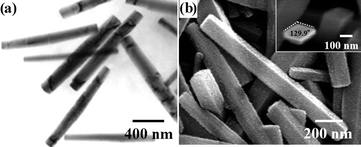 | ||
| Fig. 1 (a) TEM and (b) SEM images of GaOOH nanorods with an aspect ratio of ∼7 (inset of Fig. 1(b): a typical prism-shaped cross-section of a nanorod). | ||
The as-synthesized nanorods were characterized by XRD measurements, as shown in Fig. 2. The peaks that arose could be indexed as orthorhombic gallium oxide hydroxide (GaOOH). The lattice constants (a = 4.55, b = 9.79, c = 2.97 Å) calculated from the XRD pattern are consistent with the reported data (a = 4.58, b = 9.8, c = 2.97 Å; JCPDS file 06-180). The sharp and strong peaks in the XRD data indicate that the GaOOH nanorods were well crystallized. The ratio of the intensity between the (110) and (111) (the 2nd strongest) peaks is 5, two times larger than the theoretical ratio of 2.5, indicating the preferential orientation along the [001] direction. The electron diffraction (ED) pattern of an individual nanorod (inset in Fig. 3) further confirmed the single-crystalline structure and the [001] growth direction.
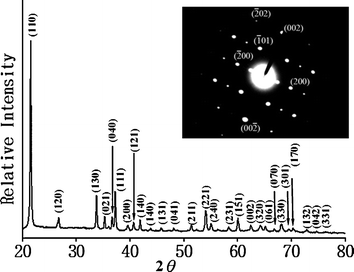 | ||
| Fig. 2 Powder XRD and the corresponding ED patterns of GaOOH nanorods with aspect ratio of ∼7. | ||
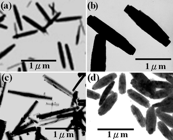 | ||
| Fig. 3 TEM images of the as-synthesized GaOOH products under various conditions: (a) 20 mmol of PVP, (b) 0.03 mmol of PVP, (c) PVP only and (d) CTAB only. | ||
Several reports have successfully employed PVP polymer as a structure-directing agent in the preparation of one-dimensional nanomaterials.29–32 All of the evidence has shown the importance of PVP in the control of nanorod growth. In this study, we adjusted the concentration of PVP to investigate the fate of GaOOH morphology (Fig. 3). With an increase of PVP from 1 mmol (Fig. 1) to 20 mmol, the GaOOH nanorods were dramatically shortened, with lengths less than 700 nm, and the lateral cross-sections were confined to the range 40–120 nm (Fig. 3(a)). On the other hand, if PVP was decreased to 0.03 mmol (Fig. 3(b)), the GaOOH morphology transformed into more spindle-like structures with longer (∼1.5 μm) and thicker sizes (∼384 nm). Although the exact PVP-assisted growth mechanism of the GaOOH nanorods is not clear, it is believed that PVP plays the function of kinetically controlling the growth rate by being preferentially absorbed on certain crystalline surfaces, leading to highly anisotropic growth. For the growth of the GaOOH nanorods, the pyrrolidone ring groups and the hydrocarbon chains of the PVP molecules are likely to be absorbed onto the {110} facets of the GaOOH nanocrystals through hydrogen bonds and/or van der Waals forces. This would result in growth along the [001] direction due to limited growth along the [110] direction. However, a too high molar concentration (20 mmol) of PVP might cause high coverage of PVP on the other faces, so, for example, confining the [001] direction growth rate in addition to {110} facets. The incomplete coverage of PVP (0.03 mmol) could not effectively passivate either end face or side surface growth. Consequently, the lateral cross-section grows prominently, as well as showing enhanced length.
Additional experiments were conducted to reveal more clearly the control of the growth of GaOOH nanorods from both CTAB- and PVP-stabilizing surfactants. Experiments with PVP only showed that the absence of CTAB favored the growth of longer GaOOH nanostructures (Fig. 3(c)). For example, nanorods longer than 1.2 μm could be readily achieved. The lateral dimensions also became randomly distributed over a wide range between 100–600 nm. Parallel experiments with CTAB only were performed under the same conditions and spindle-like structures were yielded (Fig. 3(d)). These spindle-like particles had an average length of 710 nm and an ellipsoidal width of 220 nm. These experiments clearly suggest that PVP predominately determines the formation of GaOOH nanorod structures. That is, PVP is preferentially oriented along an [001] direction by confining the side surface {110} facets. Meanwhile, the CTAB surfactant had a better effect on controlling the longitudinal growth due to passivation on the end faces. However, CTAB also took part in controlling the lateral dimension to achieve a better uniform size by incorporation with PVP.
We have seen that PVP polymer plays a role in assisting the growth of GaOOH nanorods. It is supposed that long-chain polymers might facilitate an increase in the longitudinal direction of the anisotropic nature. As compared to PVP (Mw 40000) with 360 repeating monomer units, a poly(vinyl alcohol) (Mw 22000) with 458 repeating units was introduced to synthesize GaOOH nanostructures. Fig. 4(a) shows the TEM image of PVA-assisted GaOOH nanowires. A long-chain PVA promoted highly anisotropic growth with lengths of up to 10 µm and lateral dimensions of ∼50 nm, resulting in an aspect ratio of at least 200. EDS analysis (Fig. 4) of the as-grown GaOOH identified Ga signal. The ED pattern indicated the formation of crystalline GaOOH nanowires with a 〈001〉 direction in the growth axis (Fig. 4(c) and (d)).
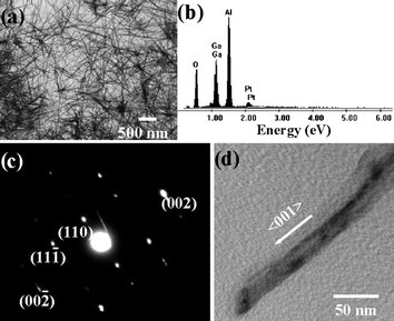 | ||
| Fig. 4 (a) TEM image, (b) EDS analysis and (c) ED pattern of GaOOH nanowires synthesized in the presence of PVA/CTAB. (d) TEM image corresponding to the ED pattern of (c). EDS measurements were carried out on an Al substrate with a Pt coating. | ||
The thermal treatments of the as-synthesized GaOOH nanowires were studied by a simple calcination process. Ga2O3 (Fig. 5) retained the same morphology as that of the GaOOH nanowires after thermal treatment. The as-prepared Ga2O3 nanowires exhibited lengths of up to 10 µm, and diameters slightly reduced to ∼38 nm for β-Ga2O3 and ∼42 nm for γ-Ga2O3, as compared to ∼50 nm for the GaOOH nanowires. The XRD pattern shows that the GaOOH nanowires were converted to a monoclinic β-Ga2O3 structure at a temperature of 750 °C over 18 h, as shown in Fig. 6(a). Calcination at 500 °C for 6 h, on the other hand, formed an F-center cubic γ-Ga2O3 structure with broadened diffraction peaks (Fig. 6(b)), which have also been reported in previous literature for crystalline γ-Ga2O3 materials.7,8,33
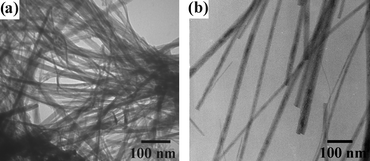 | ||
| Fig. 5 TEM images of (a) β-Ga2O3 nanowires formed by the calcination of GaOOH nanowires at a temperature of 750 °C for 18 h and (b) γ-Ga2O3 nanowires obtained by the calcination of GaOOH nanowires at a temperature of 500 °C for 6 h. | ||
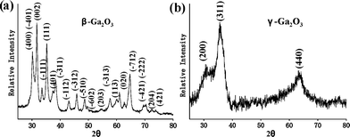 | ||
| Fig. 6 XRD spectra of (a) β-Ga2O3 nanowires formed by the calcination of GaOOH nanowires at a temperature of 750 °C for 18 h and (b) γ-Ga2O3 nanowires obtained by the calcination of GaOOH nanowires at a temperature of 500 °C for 6 h. | ||
The as-prepared β-Ga2O3 and γ-Ga2O3 nanowires were further characterized by HR-TEM images and ED patterns (Fig. 7). The reflection spots of the diffraction pattern corresponding to the marked area in Fig. 7(a) indicate well-crystallized β-Ga2O3 nanowires, with preferred growth orientation along the [100] direction. The additional HRTEM image clearly shows the lattice fringes of (002) and (400) (Fig. 7(b)). For the γ-Ga2O3 nanowires, two preferred growth orientations along [110] (Fig. 7(c)) and [121] (Fig. 7(d)) are observed. However, the presence of the elongated diffraction spots from the γ-Ga2O3 nanowires suggests non-single crystalline characteristics consisting of multiple nanocrystallites.
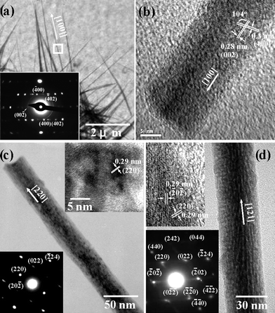 | ||
| Fig. 7 TEM images and ED patterns of (a,b) β-Ga2O3 nanowires and (c,d) γ-Ga2O3 nanowires. The insets show the corresponding ED patterns and lattice fringes of the respective nanowires. | ||
Although spindle-, rod- and wire-shaped β-Ga2O3 nanostructures have been fabricated and reported to exhibit a broad PL,1,2,5,16,17,26–28 the optical properties of GaOOH and γ-Ga2O3 nanowires remain unknown. Fig. 8(a) shows the UV-vis optical absorption of GaOOH, β-Ga2O3 and γ-Ga2O3 nanowires. An estimate of the optical band gap (Eg) can be obtained using the following equation:25,34
| (αhν)n = B(hν − Eg). |
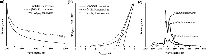 | ||
| Fig. 8 (a) UV-vis absorption spectra and (b) plot of (αEphoton)2vs. Ephoton for GaOOH, γ-Ga2O3 and β-Ga2O3 nanowires. (c) Room temperature PL spectra of GaOOH and (β-, γ-) Ga2O3 nanowires upon excitation at 280 nm. | ||
Fig. 8(c) shows the PL spectrum of β-Ga2O3 nanowires excited at 280 nm, generating two narrow blue emissions centered at 387 and 415 nm. In addition, a broad UV emission band ranging from 360 to 300 nm was observed. The GaOOH and cubic phase γ-Ga2O3 nanowires were also included in the PL investigation and excited at 280 nm, consequently producing similar luminescence peaks centered at 390 and 412 nm. Because the luminescence contour appeared to be close to that of β-Ga2O3 nanowires (Fig. 8(c)), it is reasonably assumed that these Ga-related nanowires (GaOOH, β-Ga2O3 and γ-Ga2O3) may have similar Ga–O electronic transitions in their PL mechanisms. The emission spectrum of GaOOH and γ-Ga2O3 nanocrystals are reported for the first time. As for the PL mechanism of β-Ga2O3, the blue emission could be associated with the presence of oxygen vacancies.1,2,36–38 The blue range emission is proposed to be due to either the recombination of an electron on a donor formed by oxygen vacancies and a hole on an acceptor formed by gallium vacancies or through a recombination of oxygen vacancies and acceptors of gallium–oxygen vacancy pairs.34 Furthermore, Binet and Gourier put forward a PL model for β-Ga2O3, where the blue emission originates from an excited hole on an acceptor capturing an electron in a donor oxygen vacancy, resulting in the formation of a trapped exciton.1 Meanwhile, the UV emission appears to be due to a self-trapped exciton from a detrapped electron emitting a UV photon. It is worth noting that the PL spectrum of β-Ga2O3 nanowires based on previous studies exhibited a broad band covering from the UV to the visible range.1,2,5,17,26–28 With the high-resolution synchrotron X-ray source employed in the present work, the blue emissions of the GaOOH and (β-, γ-) Ga2O3 nanowires could be resolved into a few sharp peaks, providing a valuable reference for further understanding the PL mechanisms involved.
Conclusions
A simple, low temperature, solution-phase approach has been employed to manipulate GaOOH and Ga2O3. The cationic surfactant CTAB, and polymers PVP and PVA, are requisite for the formation of nanorods and nanowires. Cationic CTAB has a greater effect on the confined growth in the longitudinal direction, while the polymers have more control over the lateral dimensions. A high-resolution synchrotron X-ray source was used to investigate the PL spectra of GaOOH and Ga2O3 nanowires, where the luminescent structures of GaOOH and γ-Ga2O3 were demonstrated for the first time. Due to the similarity in their emission contours, these gallium oxide-based nanowires are likely have similar PL mechanisms.Acknowledgements
This work was supported by the National Science Council, Taiwan. We thank Dr Bing-Ming Cheng and Mrs Hsiao-Chi Lu for valuable help with PL measurements.References
- L. Binet and D. Gourier, J. Phys. Chem. Solids, 1998, 59, 1241–1249 CrossRef CAS.
- Z. Hajnal, J. Miró, G. Kiss, F. Réti, P. Deák, R. C. Herndon and J. M. Kuperberg, J. Appl. Phys., 1999, 86, 3792–3796 CrossRef CAS.
- H. Amano, I. Akasaki, K. Hiramstsu, N. Koide and N. Sawaki, Thin Solid Films, 1988, 163, 415–420 CrossRef CAS.
- R. Roy, V. G. Hill and E. F. Osborn, J. Am. Chem. Soc., 1952, 74, 719–722 CrossRef CAS.
- H. S. Qian, P. Gunawan, Y. X. Zhang, G. F. Lin, J. W. Zheng and R. Xu, Cryst. Growth Des., 2008, 8, 1282–1287 CrossRef CAS.
- J. Zhan, Y. Bando, J. Hu, Y. Li and D. Golberg, Chem. Mater., 2004, 16, 5158–5161 CrossRef CAS.
- M. Rodríguez Delgado and C. Otero Areán, Z. Anorg. Allg. Chem., 2005, 631, 2115–2120 CrossRef.
- S. E. Collins, M. A. Baltanás and A. L. Bonivardi, J. Phys. Chem. B, 2006, 110, 5498–5507 CrossRef CAS.
- V. M. Bermudez, Langmuir, 2008, 24, 12943–12952 CrossRef CAS.
- A. P. Alivisatos, Science, 1996, 271, 933–937 CrossRef CAS.
- A. M. Morales and C. M. Lieber, Science, 1998, 279, 208–211 CrossRef CAS.
- J. Hu, T. W. Odom and C. M. Liber, Acc. Chem. Res., 1999, 32, 435–445 CrossRef CAS.
- A. C. Taş, P. J. Majewski and F. Aldinger, J. Am. Ceram. Soc., 2002, 85, 1421–1429 CrossRef CAS.
- M. Ristić, S. Popovic and S. Music, Mater. Lett., 2005, 59, 1227–1233 CrossRef CAS.
- D. Kisailus, J. H. Choi, J. C. Weaver, W. J. Yang and D. E. Morse, Adv. Mater., 2005, 17, 314–318 CrossRef CAS.
- S. Fujihara, Y. Shibata and E. Hosono, J. Electrochem. Soc., 2005, 152, C764–C768 CrossRef.
- X. H. Liu, G. Z. Qiu, Y. Zhao, N. Zhang and R. Yi, J. Alloys Compd., 2007, 439, 275–278 CrossRef CAS.
- S. G. Chen, S. M. Luo, Y. Zhou, Y. Chen, T. Q. Liu and C. G. Long, Mater. Lett., 2008, 62, 4566–4569 CrossRef CAS.
- S. Avivi, Y. Mastai, G. Hodes and A. Gedanken, J. Am. Chem. Soc., 1999, 121, 4196–4199 CrossRef CAS.
- J. Zhang, Z. Liu, C. Lin and J. Lin, J. Cryst. Growth, 2005, 280, 99–106 CrossRef CAS.
- Y. Zhao, R. L. Frost and W. N. Martens, J. Phys. Chem. C, 2007, 111, 16290–16299 CrossRef CAS.
- Y. Zhao, R. L. Frost, J. Yang and W. N. Martens, J. Phys. Chem. C, 2008, 112, 3568–3579 CrossRef CAS.
- C.-C. Huang, C.-S. Yeh and C.-J. Ho, J. Phys. Chem. B, 2004, 108, 4940–4945 CrossRef CAS.
- C.-C. Huang, C.-H. Su, M.-Y. Liao and C.-S. Yeh, Phys. Chem. Chem. Phys., 2009, 11, 6331–6334 RSC.
- C.-C. Huang, J. R. Hwu, W.-C. Su, D.-B. Shieh, Y. Tzeng and C.-S. Yeh, Chem.–Eur. J., 2006, 12, 3805–3810 CrossRef CAS.
- K. W. Chang and J. J. Wu, Adv. Mater., 2004, 16, 545–549 CrossRef CAS.
- E. G. Víllora, T. Atou, T. Sekiguchi, T. Sugawara, M. Kikuchi and T. Fu, Solid State Commun., 2001, 120, 455–458 CrossRef CAS.
- S. Cho, J. Lee, I. Y. Park and S. Kim, Mater. Sci. Eng., B, 2002, 95, 275–278 CrossRef.
- Y. Sun, B. Gates, B. Mayers and Y. Xia, Nano Lett., 2002, 2, 165–168 CrossRef CAS.
- Y. Sun, Y. Yin, B. T. Mayers, T. Herricks and Y. Xia, Chem. Mater., 2002, 14, 4736–4745 CrossRef CAS.
- J. Wang, X. Wang, Q. Peng and Y. Li, Inorg. Chem., 2004, 43, 7552–7556 CrossRef CAS.
- Y. Gao, P. Jiang, D. F. Liu, H. J. Yuan, X. Q. Yan, Z. P. Zhou, J. X. Wang, L. Song, L. F. Liu, W. Y. Zhou, G. Wang, C. Y. Wang, S. S. Xie, J. M. Zhang and D. Y. Shen, J. Phys. Chem. B, 2004, 108, 12877–12881 CrossRef CAS.
- C.-N. Lin and M. H. Huang, J. Phys. Chem. C, 2009, 113, 925–929 CrossRef CAS.
- H. Zhou, W. Cai and L. Zhang, Appl. Phys. Lett., 1999, 75, 495–497 CrossRef CAS.
- G. Sinha, K. Adhikary and S. Chaudhuri, J. Phys.: Condens. Matter, 2006, 18, 2409–2415 CrossRef CAS.
- L. Fu, Y. Liu, P. Hu, K. Xiao, G. Yu and D. Zhu, Chem. Mater., 2003, 15, 4287–4291 CrossRef CAS.
- T. Harwig and F. Kellendonk, J. Solid State Chem., 1978, 24, 255–263 CrossRef CAS.
- C. H. Liang, G. W. Meng, G. Z. Wang, Y. W. Wang, L. D. Zhang and S. Y. Zhang, Appl. Phys. Lett., 2001, 78, 3202–3204 CrossRef CAS.
| This journal is © The Royal Society of Chemistry and the Centre National de la Recherche Scientifique 2010 |