Fabrication of a cyclic olefin copolymer planar waveguide embedded in a multi-channel poly(methyl methacrylate) fluidic chip for evanescence excitation
Paul I.
Okagbare
ac,
Jason M.
Emory
ac,
Proyag
Datta
c,
Jost
Goettert
c and
Steven A.
Soper
*abc
aDepartment of Chemistry, Louisiana State University, Baton Rouge, LA 70803, USA. E-mail: chsope@lsu.edu
bDepartment of Mechanical Engineering, Louisiana State University, Baton Rouge, LA 70803, USA
cCenter for BioModular Multi-Scale Systems, Louisiana State University, Baton Rouge, LA 70803, USA
First published on 4th November 2009
Abstract
The fabrication and characterization of a novel cyclic olefin copolymer (COC) waveguide embedded in a poly(methyl methacrylate), PMMA, fluidic chip configured in a multi-channel format with an integrated monolithic prism for evanescent fluorescence excitation are reported. The fabrication approach allowed the embedded waveguide to be situated orthogonal to a series of fluidic channels within the PMMA wafer to sample fluorescent solutions in these channels using the evanescence properties of the waveguide. Construction of the device was achieved using several fabrication techniques including high precision micromilling, hot embossing and stenciling of a polymer melt to form the waveguide and coupling prism. A waveguide channel was fabricated in the fluidic chip's cover plate, also made from PMMA, and was loaded with a COC solution using a pre-cast poly(dimethylsiloxane), PDMS, stencil containing a prism-shaped recess. The PMMA substrate contained multiple channels (100 µm wide × 30 µm deep with a pitch of 100 µm) that were situated orthogonal to the waveguide to allow penetration of the evanescent field into the sampling solution. The optical properties of the waveguide in terms of its transmission properties and penetration depth of the evanescent field in the adjacent solution were evaluated. Finally, the device was used for laser-induced fluorescence evanescent excitation of a dye solution hydrodynamically flowing through multiple microfluidic channels in the chip and processed using a microscope equipped with a charge-coupled device (CCD) for parallel readout. The device and optical system were able to image 11 channels simultaneously with a limit-of-detection of 7.1 × 10⁻²⁰ mol at a signal-to-noise ratio of 2. The waveguide was simple to manufacture and could be scaled to illuminate much higher channel numbers making it appropriate for high-throughput measurements using evanescent excitation.
Introduction
Lab-on-a-chip (LOC) systems offer a number of compelling advantages compared to their conventional bench-top counterparts, including the ability to process large amounts of chemical/biochemical information due to the ability to build chips in a highly parallel format and the high processing speed they offer.1–6 A major challenge associated with these miniaturized, multi-channel systems is the associated ultra-small sampling volumes, which places a high demand on the detection system to provide the required limit-of-detection for interrogating a few molecules present in these small detection volumes. While several detection modalities exist for microfluidic systems,7,8 laser-induced fluorescence (LIF) has been widely adopted due to the high sensitivity, selectivity and extremely low limits-of-detection obtainable.9,10Classical optical configurations for LIF are often based on epi-illumination formats,11,12 in which both excitation and fluorescence light propagate in the same optical path with spectral sorting accomplished using dichroic filters. Another optical configuration, which has found applications in LIF detection, is total internal reflection (TIR) fluorescence,13–15 in which fluorescent samples are excited using a surface-confined excitation field. Several reports have documented the use of TIR optics, which use prisms,16–18 microscope objectives,19,20 or optical fibers.21,22 In all cases, fluorescence excitation utilized the evanescent field generated by TIR at a high refractive index to a low refractive index boundary.
The penetration depth of the evanescent field is usually fairly small (<750 nm) with the absolute value dependent upon the excitation wavelength, the refractive indices of the waveguiding material and substrate, and the launch angle of the incident light. The intensity of the evanescent field, which is proportional to the square of the electric field amplitude,23 normally drops off exponentially into the lower index medium, thus enabling the realization of small excitation volumes.
A common class of materials used for TIR fluorescence is optical waveguides,24,25 which offer advantages such as the realization of compact sensing elements suitable for LOC applications and the potential for fabricating multiple sensors on a single chip.26 Planar waveguides for biosensing have been made using a variety of materials, such as metal films,27 metal oxide films,28 photonic crystals,29,30 or silicon oxynitride.31 While glass remains the most commonly used material for waveguide applications,15,32 its incorporation into other sample processing units required for LOC sensing is a challenge due to its limited and sometimes costly fabrication modalities. As a result, polymer-based waveguides33,34 have attracted much interest because of their simple fabrication characteristics and in some cases, their favorable optical properties.35 Also, the ease of integrating these materials into instruments suitable for point-of-care (POC) applications is of great value.
Several polymer materials have been employed for waveguiding including poly(dimethylsiloxane) (PDMS),36,37 SU-8,26,38–40 and poly(methyl methacrylate) (PMMA).41 As an example, Xu et al.41 recently demonstrated the use of a PMMA-based air-embedded planar waveguide for reading DNA microarrays. This waveguide was fabricated in a single step using double-sided hot embossing from two metal mold masters. Another polymeric material, which holds promise as a potential waveguide material, is cyclic olefin copolymer (COC). COC has properties that can be tailored within a wide range of physicochemical characteristics during polymerization.42 COC possesses high optical transparency, excellent electrical properties, high rigidity, good biocompatibility, high chemical resistance to acids and alkalis and good thermal properties.42,43 Several works have reported on the microfabrication of COC devices,44–49 which have created avenues for expanding the utility of this polymer, especially as a waveguide material due to its exquisite optical properties and the fact that the optical properties, such as the refractive index, can be tuned by adjusting the percent composition of the monomer comprising the copolymer.50
Although progress has been made toward integrating waveguides into microfluidic systems,14,51–53 the effective propagation of light through a single planar waveguide for evanescent excitation of multiple fluidic channels suitable for high-throughput fluorescence analyses has not been reported to date. In this paper, we present for the first time the fabrication of a polymer waveguide embedded in a lower refractive index polymer serving as a cover plate for a substrate that contained a series of fluidic channels. The waveguide was situated orthogonal to the microfluidic channels to provide evanescent excitation of the material moving through the fluidic channels. The fluidic channels were hot embossed from a metal master into a PMMA sheet, which was thermally fusion bonded to a PMMA cover plate containing the orthogonal COC waveguide. To carefully control the laser launch angle into the waveguide near the critical angle, which was defined by the refractive index of COC (n = 1.53) and PMMA (n = 1.48), a monolithic prism was integrated to the COC waveguide in a single fabrication step eliminating the need for an external prism and index matching oil.
Experimental
Materials and reagents
COC sheets (grade: 5010L; Tg = 110 °C; n = 1.53) were obtained from Topas (Topas Advanced Polymer, USA); the molecular structure of Topas COC is shown in Fig. 1a with the monomer units represented as x and y. Toluene was obtained from Fisher Scientific (Fisher Chemicals, USA) and used as supplied to make a polymer solution of COC, which was obtained by dissolving pieces of COC in toluene. A PDMS base and curing agents were obtained from Dow Corning (Dow Corning Corporation, Midland, USA). AlexaFluor 647 was obtained from Molecular Probes (Eugene, Oregon, USA) with stock and sample solutions made in 1× Tris–Taps–EDTA (TTE) buffer (pH = 8.7).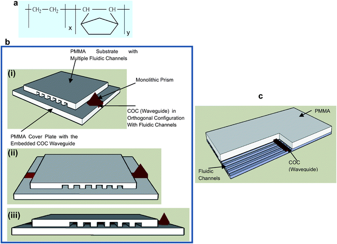 | ||
| Fig. 1 (a) Molecular structure of Topas COC; x and y represent the monomer units, which are polymerized by metallocene catalyzed polymerization. The Tg and the refractive index, n, can be modified by increasing or decreasing the amount of norbornene (y) units in the monomer mixture during polymerization. (b) Schematic representation of the fluidic device with embedded COC planar waveguide with a monolithic coupling prism: (i) diagonal view, (ii) frontal view, and (iii) cross-sectional view. (c) Schematic representation of a portion of the device showing the multi-channel fluidic architecture and interconnected waveguide. | ||
Image acquisition
All fluorescence images were acquired using a Roper Scientific (Trenton, NJ) Spec-10 charge-coupled (CCD) camera that was thermally cooled to −90 °C and contained a 1 MHz digital converter. The CCD camera had 20 µm pixels that were configured in a 1340 × 100 back-illuminated format. Scanning electron micrograph (SEM) images were acquired using a Cambridge S-260 SEM (Cambridge instruments Ltd. Cambridge, UK) interfaced to Video Wave 5 (Real Networks Inc. Washington, USA). Atomic force microscopy (AFM) images were acquired using a Nanoscope III instrument (Digital Instruments, CA).Layout of the waveguide and fluidic network
Fig. 1b shows a schematic diagram of the multi-channel fluidic device with an embedded COC waveguide and monolithic prism. The device consisted of two layers: a PMMA cover plate (refractive index, n, = 1.48, Tg = 107 °C) into which the COC waveguide (n = 1.53) was embedded and a PMMA substrate, which contained the fluidic channels (100 µm × 30 µm) that were replicated/embossed from a metal mold master (see Fig. 1c). The waveguide (200 µm × 200 µm) was situated orthogonal to the longitudinal axis of the fluidic channels along the width of the PMMA cover plate, the size of which defined the excitation volume in each fluidic channel along with the penetration depth of the evanescent field. The monolithic prism (see Fig. 1b) facilitated coupling the excitation light into the waveguide without the need for an external prism or index matching oil.Fabrication of the embedded waveguide
The stepwise fabrication process for creating the embedded COC orthogonal planar waveguide and monolithic prism is shown in Fig. 2a. The first step involved the generation of a PDMS stencil, which was used to define the waveguide and coupling prism and was produced by casting the PDMS against a relief. The relief contained a prism-shaped structure that was aligned to a 1 mm diameter pole structure (height of structure = 2.0 mm) used to create an access reservoir. The plastic relief was replicated from a brass mold master fabricated by high precision micromilling (Kern MMP micromilling machine).54,55 A PDMS pre-polymer solution was obtained by mixing the PDMS base and the curing agent at a ratio of 10 : 1 by mass. This solution was degassed and loaded through the injection port of a molding frame containing the relief to completely fill the mold cavity (see (i) in Fig. 2a). Curing of the PDMS pre-polymer solution was achieved in 1.5 h using a vacuum oven set at 70 °C. The resulting PDMS stencil containing the prism-shaped recess and a 1 mm diameter reservoir (created by the 1 mm diameter pole) was peeled from the relief (see (ii) in Fig. 2a).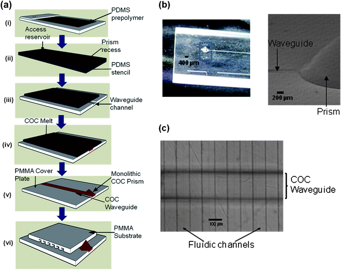 | ||
| Fig. 2 (a) Schematic representation of the stepwise process for the fabrication of the embedded COC orthogonal waveguide in a PMMA chip. A relief was used for casting a PDMS pre-polymer (PDMS + curing agent at 10 : 1 ratio) to form the stencil, which contained the recess for molding the COC prism and an access reservoir to allow filling of the COC melt (i). The PDMS stencil was peeled from the relief after curing at 70 °C for 90 min (ii) and placed on the surface of a PMMA sheet, which would serve as the device cover plate, containing a pre-fabricated waveguide channel (waveguide channel was embossed from a mold master fabricated using high precision micromilling) (iii) and a COC melt (prepared using toluene as the solvent) was introduced into the assembly to form the waveguide and coupling prism (iv). The PDMS stencil was then peeled off from the PMMA cover plate, which created the embedded waveguide with the monolithic coupling prism (v). Finally, the PMMA cover plate with waveguide assembly was thermal fusion bonded to a PMMA substrate containing multiple fluidic channels (vi) that were prepared using hot embossing. The fluidic substrate and the PMMA cover plate were thermally fusion bonded at ∼105 °C, near the Tg of both polymeric materials. (b) Photographs of the PMMA sheet showing the embedded waveguide with the integrated monolithic prism (to the right is the SEM of a section of the prism). (c) Optical micrograph of the embedded waveguide integrated to the fluidic channels. | ||
The PDMS stencil was then placed onto a sheet of PMMA containing a pre-fabricated waveguide channel (200 µm × 200 µm) (see (iii) in Fig. 2a). The waveguide channel was replicated onto a sheet of PMMA from a brass mold master that was fabricated by high precision micromilling. The prism-shaped recess on the PDMS stencil and the access reservoir were carefully aligned with the waveguide channel under a microscope. A COC solution (melt) was then introduced into the waveguide channel through the access reservoir in the PDMS stencil to fill the channel and the prism-shaped recess (see (iv) in Fig. 2a). This assembly was allowed to cure in a vacuum oven for 24 h at room temperature. Following curing of the COC, the PDMS stencil was carefully peeled from the PMMA sheet, which formed the embedded COC waveguide and the monolithic coupling prism (see (v) in Fig. 2a). Fig. 2b shows an image of the embedded COC waveguide with monolithic prism.
Integration of the embedded waveguide with the multi-channel substrate
The fluidic channels were replicated into a PMMA substrate (thickness = 250 µm) via hot embossing from a brass mold master, which was fabricated by high precision micromilling.54,55 This PMMA wafer contained channels with dimensions of 100 µm width × 30 µm depth and was thermally fusion bonded to the waveguide-bearing PMMA cover plate in an orthogonal configuration with the waveguide spanning the length of the entire array of fluidic channels (see (vi) in Fig. 2a). In this case, the embedded waveguide defined the illumination area for each fluidic channel. Fig. 2c shows an optical micrograph of the waveguide and the fluidic channel when thermally assembled.Water absorption measurements
The COC polymer was prepared for water absorption measurements by coating a portion of the COC melt onto a glass slide to a thickness of 200 µm. The COC coated glass slide was then placed into a vacuum oven for 24 h at room temperature. Following curing, the polymer film was extracted for water absorption measurements. The polymer films were heated to 95 °C for 50 min, allowed to cool to room temperature, and subsequently weighed. The sample was then immersed into water for 24 h at room temperature and re-weighed following drying under a constant flow of N2 to remove surface moisture. The difference in weight was calculated in order to establish the percentage of water absorption.50Coupling of light into the waveguide
The excitation laser (635 nm) was generated from a laser diode (HL6322G Hitachi Laser Diode, Thorlabs) and coupled into a fiber optic cable (AFS50/125Y, Thorlabs), which at its distal end was coupled to an OFR fiber port (PAF-X-2-B) equipped with a collimation lens to generate a collimated laser beam. To minimize light loss at the entrance to the waveguide, the collimated laser beam was passed through a beam expander that was used in the reverse mode to reduce the beam diameter from 2 mm to ∼200 µm. The resulting beam (4.4 mW) was launched through the monolithic prism into the waveguide with a launch angle adjusted to ∼76° (critical angle θc = 75°) using a goniometer, which allowed the light to propagate through the waveguide via total internal reflection. The critical angle (θc = sin−1nclad/ncore) was defined by the refractive indices of the PMMA cladding (n = 1.48) and the COC core (n = 1.53).Results and discussion
Evaluation and characterization of the embedded COC waveguide
To confirm that loading of the waveguide channel with the COC melt generated an optically homogeneous interface between the COC core and PMMA after curing the COC, a SEM of the empty waveguide channel and the COC filled channel were obtained (data not shown). In addition, we also inspected via optical microscopy the COC core for any in-homogeneities resulting from air bubbles that may create speckle patterns in the waveguide due to refractive index changes. Close examination of the SEMs revealed a highly uniform interface between the COC and PMMA with no observable imperfections in the COC core. These results were further supported by AFM images (see Fig. 3a) of the surface of the embedded waveguide, which generated a RMS value (surface roughness) of 61.2 ± 0.1 nm. As can be seen from this image, the COC core surface was smooth and showed no evidence of large pits arising from air bubbles or other materials during its production, which could generate light loss. We also noticed no speckles in the waveguide when light was coupled into it.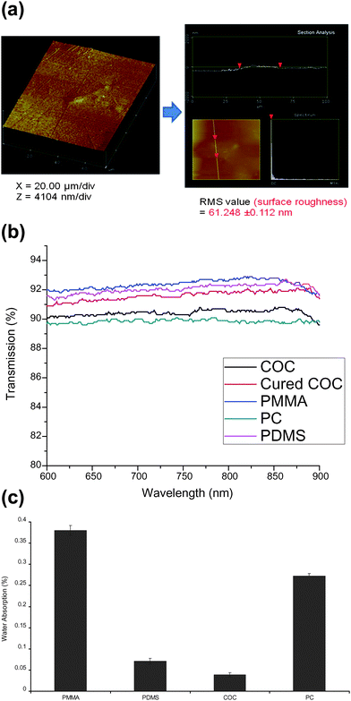 | ||
| Fig. 3 (a) Left: AFM image of the surface of the cured COC planar polymer waveguide embedded in sheet PMMA; z-scale is 4104 nm per div., and x-scale is 20 µm per div. Right: section analysis of the waveguide surface; top panel shows the surface roughness with RMS = 61.248 ± 0.112 nm. (b) Optical transmission spectra (600 nm–900 nm) of COC (black), cured COC waveguide (red), PMMA (blue), PC (polycarbonate) (green) and PDMS (purple). (c) Moisture resistance of COC compared to other polymers. | ||
Among the properties of waveguides that define their suitability for efficient operation is their optical transparency at different wavelengths. This is particularly important for fluorescence applications because light loss due to optical absorption by the waveguide can give rise to autofluorescence that can degrade the signal-to-noise ratio in any sensitive fluorescence measurement.35 Therefore, transmission spectra were collected between 600 and 900 nm for both the native COC sheet material and the cured COC core waveguide. A comparison of the transmission properties of COC was made to other potential polymeric waveguiding materials as well. The results of these measurements can be seen in Fig. 3b. COC showed high optical transparency (∼91%) across the entire wavelength range interrogated. In addition, there was no significant difference in the transmission spectrum obtained for native COC and the cured COC waveguide. This indicated that the fabrication procedure did not impact the optical properties of COC preserving its high optical transparency, making it suitable for sensitive fluorescence applications.
Water absorption is also a critical issue in selecting proper waveguide materials because water absorption can change the refractive index of the material inducing light loss or specularly scattered radiation increasing the background in any optical measurement. Therefore, an investigation of the moisture resistance of the embedded COC waveguide was carried out. A COC melt was spin-coated onto a glass slide, dried, weighed, soaked in water and then re-weighed as described in the Experimental section. Films of other polymers were also processed in a similar fashion, but using a solvent in which each particular polymer showed high solubility. Fig. 3c shows the water absorption characteristics of COC and other polymer films with COC providing the highest moisture resistance. This result could be explained based on COC's more hydrophobic nature compared to the other investigated materials. The high moisture resistance of COC indicates that it will maintain stable optical properties, especially its refractive index, during the fluorescence measurements even though the waveguide is in contact with the interrogating solution (see Fig. 1b).
Another important optical characteristic of waveguides is their transmission efficiency. We measured light attenuation in decibels (dB) per unit length (cm) using the equation:
| A = −10log (Pout/Pin) × 1/L | (1) |
As mentioned earlier, propagation of light through a planar waveguide generates an evanescent electromagnetic field, which penetrates into the surrounding medium with an amplitude that decays exponentially with distance from the interface. The penetration depth (at the 1/e intensity) of the evanescent field can be estimated with respect to the launch angle from the expression:56
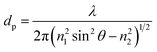 | (2) |
We evaluated the ability of our embedded polymer waveguide for efficient fluorescence excitation into the adjacent solution by depositing 20 µL of a 1 µM solution of AlexaFluor 647 onto the waveguide and placing a thin cover slip on the surface with a spacer to provide a uniform thickness of fluid above the waveguide. Laser light (λ = 635 nm) was launched into the embedded waveguide through the prism and fluorescent signals were collected at different launch angles using a 2× microscope objective to image the entire length (see top panel of Fig. 4) of the waveguide onto a CCD camera (exposure time = 1 s). Fig. 4 shows a plot of the fluorescence intensity as a function of launch angle. As can be seen, the highest fluorescence intensity was obtained at a launch angle of 76°, which is close to the critical angle of this waveguide. We also plotted eqn (2) (see solid blue line in Fig. 4) to show the decay in dp as a function of launch angle. As can be seen from this plot, the results from eqn (2) agreed with the observed trend in the fluorescence yield, indicating that the decrease in fluorescence intensity was most likely due to the effective decrease in the sampling zone defined by the evanescent field thickness. The modest agreement at launch angles below 82° most likely resulted in errors associated with adjusting the launch angle in this region because abrupt changes in dp occur with slight changes in θ. Measurements carried out below 75° showed negligible levels of fluorescence (data not shown). This is expected because the laser light did not undergo total internal reflection when launched at angles below the critical angle.
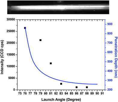 | ||
| Fig. 4 The top panel shows a typical fluorescence image acquired with the CCD when light was launched into the waveguide with a fluorescent solution sandwiched between a cover slip and the COC waveguide surface. The bottom panel shows the resultant fluorescence intensity at different launch angles. The solid blue line represents the penetration depth plotted as a function of the launch angle using eqn (2). | ||
Fluorescence measurements from orthogonal microfluidic channels
The ability to utilize the waveguide and fluidic architecture after assembly for fluorescence measurements in a multi-channel format was demonstrated by hydrodynamically pumping fluorescent solutions through the fluidic channels (see Fig. 2c) using a 100 nM solution of AlexaFluor 647 and reading the fluorescence signal from each fluidic channel with the CCD (relay optic was a 10× objective, NA = 0.5). The results of these measurements are shown in Fig. 5.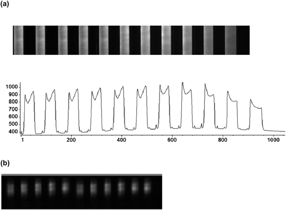 | ||
| Fig. 5 (a) Fluorescence image acquired from multiple fluidic channels (11 microchannels shown) filled with 100 nM AlexaFluor 647 when light was launched into the COC planar waveguide through the monolithic prism; there was a clear distinction between channels (with sample) showing fluorescence signal with fairly uniform intensity (bottom panel) and the inter-channel area showing dark background. The image was acquired with a 10× microscope objective (NA = 0.5). (b) Fluorescence image from the same device acquired with a 2× microscope objective (NA = 0.1) to clearly show the waveguide geometry. | ||
In Fig. 5a, a fluorescence image from 11 microchannels (100 µm wide × 30 µm deep with a 100 µm pitch) is shown with a clear demarcation between the dye-filled channels and the inter-channel space, which showed negligible fluorescence signal. The fluorescence generated using a 100 nM dye solution produced an SNR (signal-to-noise ratio) of 25. It is important to note that the background signal registered in this image is primarily due to camera bias and electronic offset. This bias is stable and can be subtracted from the image using a zero exposure time as background.57 We determined that the SNR was ∼48 after this bias was removed. With the volume interrogated in this fluorescence measurement, which is defined by the dimensions of the waveguide and the fluidic channel and the depth of the evanescent field (100 µm × 200 µm × 0.87 µm at a launch angle of 76°; ∼17 pL sampling volume), the optical system could detect 7.1 × 10⁻²⁰ mol at SNR = 2 or ∼42![[thin space (1/6-em)]](https://www.rsc.org/images/entities/char_2009.gif) 000 molecules occupying the sampling volume. We should note that we are using a relatively low NA objective in this case, which provides low light gathering ability. The use of higher NA relay objective would significantly increase the signal-to-noise in these measurements, but also reduce the field-of-view of the optical system.
000 molecules occupying the sampling volume. We should note that we are using a relatively low NA objective in this case, which provides low light gathering ability. The use of higher NA relay objective would significantly increase the signal-to-noise in these measurements, but also reduce the field-of-view of the optical system.
Artifacts and imperfections in the wall of the fluidic channels generated some speckles along the fluidic channel walls, which were partially responsible for the high levels of apparent fluorescence along the edges of the channel/solution interface. We can potentially reduce this artifact by improving the fabrication process of the fluidic channels by reducing surface roughness of the channel walls. For example, employing UV-lithography in conjunction with LiGA (lithography, electroplating and molding) for generating the mold master would produce sidewalls with significantly less surface roughness compared to micromilling.58 We also note that slight variations in the measured fluorescence intensity across the effective field-of-view comprising the multiple fluidic channels are partially a result of the non-flatness of the collection field by the relay microscope objective, which in this case does not have a high ‘flatness of field’ value. Implementation of an improved optical system with a wide field-of-view with a high flatness factor would improve intensity uniformity.
To clearly visualize the waveguide geometry for collecting fluorescence from the fluidic channels using evanescent excitation of the intervening solution contained in the channels, a lower magnification objective (2×, NA = 0.1) was used to acquire a second image. Fig. 5b shows this fluorescence image from each fluidic channel with the region outside the waveguide area showing a relatively dark background. This indicated that fluorescence excitation was confined only to the area corresponding to the waveguide, which generated the evanescent field.
Conclusion
We have fabricated and evaluated a novel COC planar waveguide embedded into a PMMA cover plate that was situated orthogonal to multiple fluidic channels and sampled the resulting fluorescence in the channels via evanescent excitation. The geometry employed for this COC waveguide and the fluidic network can be configured to allow matching the excitation area with the dimensions of the collection optics and array detector. The design reported herein allowed for fluorescence detection from the multiple fluidic channels using evanescent excitation and a CCD camera for parallel readout. The use of a monolithic prism allowed for precise control of the laser launch angle into the waveguide to provide sampling via the evanescent field. The launch angle was found to play a critical role in achieving high sampling efficiency by maximizing the penetration depth of the evanescent field into the adjoining solution. While the sampling efficiency is rather modest in the present case (100% × 0.87/30 ≈ 3%), this can be improved by matching the fluidic channel depth to the depth of penetration of the evanescent field.This design generated an evanescent field for the wide field excitation of fluorescent solutions traveling above the waveguide in fluidic channels, which enabled reading fluorescence signals from multiple fluidic channels in a parallel format using a CCD camera. This technology may be particularly attractive for high-throughput or multiplexed sample analyses and point-of-care applications due to the simplicity in design and fabrication. In the present studies, we monitored fluorescence produced from 11 fluidic channels. However, this throughput could be dramatically improved by reducing the channel width and also the channel pitch. For example, if we match the channel width to the CCD pixel size as well as the channel pitch, we could monitor ∼670 fluidic channels for an optical system with 1× magnification.
In future studies, the waveguide described herein will be integrated to a high density fluidic network possessing multiple channels for high-throughput screening of biochemical reactions for drug discovery applications. While the present design provides for the ability to build inexpensive microfluidic devices with integrated optics, future work will also investigate alternative steps to further reduce fabrication complexity. For example, the use of double injection molding can produce the embedded waveguide within the cover plate in a single step.59 Other future design implementations will include lenses into the integrated device to facilitate coupling of the fluorescence signal to array detectors.
Acknowledgements
The authors acknowledge support of this work through the National Institutes of Health (EB-006639), the National Science Foundation (EPS-0346411) and the Louisiana Board of Regents.References
- D. R. Reyes, D. Iossifidis, P. A. Auroux and A. Manz, Anal. Chem., 2002, 74, 2623–2636 CrossRef CAS.
- P. A. Auroux, D. Iossifidis, D. R. Reyes and A. Manz, Anal. Chem., 2002, 74, 2637–2652 CrossRef CAS.
- T. Vilkner, D. Janasek and A. Manz, Anal. Chem., 2004, 76, 3373–3385 CrossRef CAS.
- M. G. Whitesides, Nature, 2006, 442, 368–373 CrossRef CAS.
- S. P. Dittrich, K. Tachikawa and A. Manz, Anal. Chem., 2006, 78, 3887–3907 CrossRef CAS.
- J. West, M. Becker, S. Tombrink and A. Manz, Anal. Chem., 2008, 80, 4403–4419 CrossRef CAS.
- W. R. Vandaveer, S. A. Pasas-Farmer, D. J. Fischer, C. N. Frankenfeld and S. M. Lunte, Electrophoresis, 2004, 25, 3528–3549 CrossRef.
- K. B. Mogensen, H. Klank and J. P. Kutter, Electrophoresis, 2004, 25, 3498–3512 CrossRef CAS.
- L. Tao and T. R. Kennedy, Trends Anal. Chem., 1998, 17, 484–491 CrossRef.
- C. Gooijer, S. J. Kok and F. Ariese, Analusis, 2000, 28, 679–685 CrossRef CAS.
- L. G. Duveneck, P. A. Abel, A. M. Bopp, M. G. Kresbach and M. Ehrat, Anal. Chim. Acta, 2002, 469, 49–61 CrossRef CAS.
- R. Bermini, N. Cennamo, A. Minardo and L. Zeni, IEEE Sens. J., 2006, 6, 1218–1226 CrossRef.
- M. N. Kronick and W. A. Little, J. Immunol. Methods, 1975, 8, 235–240 CrossRef CAS.
- K. E. Sapdford, Y. S. Shubin, J. B. Delehanty, J. P. Golden, C. R. Taitt, L. C. Shriver-Lake and F. S. Ligler, J. Appl. Microbiol., 2004, 96, 47–58 CrossRef CAS.
- C. R. Taitt, G. P. Anderson and F. S. Ligler, Biosens. Bioelectron., 2005, 20, 2470–2487 CrossRef CAS.
- W. E. Moerner, E. J. G. Peterman, S. Brasselet, S. Kummer and R. M. Dickson, Cytometry, Part A, 1999, 36, 232–238 Search PubMed.
- N. X.-H. Xu and S. Y. Edward, Science, 1998, 281, 1650–1653 CrossRef CAS.
- X.-H. Xu and S. Y. Edward, Science, 1997, 275, 1106–1109 CrossRef CAS.
- M. F. Paige, E. J. Bjerneld and W. E. Moerner, Single Molecules, 2001, 2, 191–201 CrossRef CAS.
- W. P. Ambrose, P. M. Goodwin and J. P. Nolan, Cytometry, Part A, 1999, 36, 224–231 Search PubMed.
- M. Mehrvar, C. Bis, J. M. Scharer, M. Moo-Young and J. H. Luong, Anal. Sci., 2000, 16, 677–692 CAS.
- X. Fang and W. Tan, Anal. Chem., 1999, 71, 3101–3105 CrossRef CAS.
- W. E. Moerner and D. P. Fromm, Rev. Sci. Instrum., 2003, 74, 3597–3619 CrossRef CAS.
- A. R. Potyrailo, E. S. Hobbs and M. G. Hieftje, Fresenius' J. Anal. Chem., 1998, 362, 349–373 CrossRef CAS.
- H. M. Grandin, B. Stadler, M. Textor and J. Voros, Biosens. Bioelectron., 2006, 21, 1476–1482 CrossRef CAS.
- B. H. Ong, X. Yuan, Y. Y. Tan, R. Irawan, X. Fang, L. Zhang and S. C. Tjin, Lab Chip, 2007, 7, 506–512 RSC.
- W. L. Barnes, A. Dereux and T. W. Ebbesen, Nature, 2003, 424, 824–830 CrossRef CAS.
- W. Budach, P. A. Abel, E. A. Bruno and D. Neuschafer, Anal. Chem., 1999, 71, 3347–3355 CrossRef CAS.
- M. Pawlak, E. Schick, M. A. Bopp, M. J. Schneider, P. Oroszlan and M. Ehrat, Proteomics, 2002, 2, 383–393 CrossRef CAS.
- J. Arentoft, T. Sondergaard, M. Kristensen, A. Boltasseva, M. Thorhauge and L. Frandsen, Electron. Lett., 2002, 38, 274–275 CrossRef CAS.
- T. E. Plowman, J. D. Durstchi, H. K. Wang, D. A. Christensen, J. N. Herron and W. M. Reichert, Anal. Chem., 1999, 71, 4344–4352 CrossRef CAS.
- C. A. Rowe, L. M. Tender, M. J. Feldstein, J. P. Golden, S. B. Scruggs, B. D. MacCraith, J. J. Cras and F. S. Ligler, Anal. Chem., 1999, 71, 3846–3852 CrossRef CAS.
- J. T. Ives and W. M. Reichert, Appl. Spectrosc., 1988, 42, 68–72 CrossRef CAS.
- W. M. Reichert, J. T. Ives, P. A. Suci and V. Hlady, Appl. Spectrosc., 1987, 41, 636–640 CAS.
- H. Shadpour, H. Musyimi, J. F. Chen and S. A. Soper, J. Chromatogr., A, 2006, 1111, 238–251 CrossRef CAS.
- C. L. Bliss, J. N. McMullin and C. J. Backhouse, Lab Chip, 2007, 7, 1280–1287 RSC.
- A. D. Chang-Yen, K. R. Eich and K. B. Gale, J. Lightwave Technol., 2005, 23, 2088–2093 CrossRef CAS.
- M. A. Powers, S. T. Koev, A. Schleunitz, H. M. Yi, V. Hodzic, W. E. Bentley, G. F. Payne, G. W. Rubloff and R. Ghodssi, Lab Chip, 2005, 5, 583–586 RSC.
- S. H. Huang and F. G. Tseng, J. Micromech. Microeng., 2005, 15, 2235–2242 CrossRef.
- S. Balslev, A. M. Jorgensen, B. Bilenberg, K. B. Mogensen, D. Snakenborg, O. Geschke, J. P. Kutter and A. Kristensen, Lab Chip, 2006, 6, 213–217 RSC.
- F. Xu, P. Datta, H. Wang, S. Gurung, M. Hashimoto, S. Wei, J. Goettert, R. L. McCarley and S. A. Soper, Anal. Chem., 2007, 79, 9007–9013 CrossRef CAS.
- W. J. Huang, F. C. Chang and P. P. J. Chu, Polymer, 2000, 41, 6095–6101 CrossRef CAS.
- G. Khanarian and H. Celanese, Opt. Eng., 2001, 40, 1024–1029 CrossRef CAS.
- K. C. Fredrickson, J. Microelectromech. Syst., 2006, 15, 1060–1068 CrossRef CAS.
- B. M. Esch, S. Kapur, G. Irizarry and V. Genova, Lab Chip, 2003, 3, 121–127 RSC.
- P. Mela, A. Berg van den, B. E. Cummings, A. B. Simmons and J. B. Kirby, Electrophoresis, 2005, 26, 1792–1799 CrossRef CAS.
- G. C. Koh, W. Tan, M.-Q. Zhao, J. A. Ricco and F. Z. Hugh, Anal. Chem., 2003, 75, 4591–4598 CrossRef CAS.
- Q. Pu, O. Oyesanya, B. Thompson, S. Liu and C. J. Alvarez, Langmuir, 2007, 23, 1577–1583 CrossRef CAS.
- B. T. Stachowiak, A. D. Mair, G. T. Holden, J. L. Lee, F. Svec and M. J. J. Frechet, J. Sep. Sci., 2007, 30, 1088–1093 CrossRef CAS.
- S. J. Hwang and H. H. Yu, Jpn. J. Appl. Phys., Part 1, 2005, 44, 2541–2545 CrossRef CAS.
- H. Schmidt and A. R. Hawkins, Microfluid. Nanofluid., 2008, 4, 3–16 CrossRef CAS.
- K. B. Mogensen, N. J. Petersen, J. Hubner and J. P. Kutter, Electrophoresis, 2001, 22, 3930–3938 CrossRef CAS.
- K. B. Mogensen, J. El-Ali, A. Wolff and J. P. Kutter, Appl. Opt., 2003, 42, 4072–4079 CrossRef CAS.
- M. L. Hupert, J. W. Guy, S. D. Llopis, C. Situma, S. Rani, D. E. Nikitopoulos and S. A. Soper, Proc. SPIE–Int. Soc. Opt. Eng., 2006, 6112, 61120B-1–61120B-12.
- M. L. Hupert, J. W. Guy, S. D. Llopis, H. Shadpour, S. Rani, D. E. Nikitopoulos and S. A. Soper, Microfluid. Nanofluid., 2007, 3, 1–11 CAS.
- M. Ahmad and L. L. Hench, Biosens. Bioelectron., 2005, 20, 1312–1319 CrossRef CAS.
- G. Karl, Springer Series on Fluorescence, Standardization and Quality Assurance in Fluorescence Measurement, Quantitative Fluorescence Microscopy: Considerations and Controls, Springer, Berlin, Heidelberg, 2008, vol. 6, pp. 55–68 Search PubMed.
- M. L. Hupert, W. J. Guy, S. D. Llopis, H. Shadpour, S. Rani, D. E. Nikitopoulos and S. A. Soper, Microfluid. Nanofluid., 2007, 3, 1–11 CAS.
- C. M. Vaz, P. F. N. M. van Doeveren, R. L. Reis and A. M. Cunha, Polymer, 2003, 44, 5983–5992 CrossRef CAS.
| This journal is © The Royal Society of Chemistry 2010 |