Solvent additives and their effects on blend morphologies of bulk heterojunctions
Teddy
Salim
a,
Lydia Helena
Wong
a,
Björn
Bräuer
b,
Roopali
Kukreja
b,
Yong Lim
Foo
c,
Zhenan
Bao
d and
Yeng Ming
Lam
*ac
aSchool of Materials Science and Engineering, Nanyang Technological University, Blk N4.1, Nanyang Avenue, Singapore 639798. E-mail: ymlam@ntu.edu.sg
bStanford Institute for Materials and Energy Science, Stanford University, CA 94025, USA
cInstitute of Materials Research and Engineering (IMRE), Agency for Science and Technology and Research (A*STAR), 3 Research Link, Singapore 117602
dDepartment of Chemical Engineering, Stanford University, Stanford, CA 94305, USA
First published on 18th October 2010
Abstract
Controlling the blend morphology is one of the ways to achieve high power conversion efficiency in organic bulk heterojunction (BHJ) photovoltaic devices. One simple yet effective method is “solvent additive” approach, which involves the addition of a small fraction of high boiling point solvent into the blend of donor/acceptor dissolved in another host solvent. Even though this method has been successfully applied in a number of polymer/fullerene BHJ devices, the selection rule of the choice of additive and the host solvent has yet to be fully established. In this work, we performed a systematic study of the effect of alkyl lengths of alkanedithiol additives on the nanoscale phase separation of P3HT:PC61BM blends and consequently, the power conversion efficiency (PCE) of the devices. The extent of the additive-induced phase separation is related to the additive boiling point and the degree of interaction between the additive and fullerene, as evident from grazing incidence X-ray diffractometry (GIXRD) and scanning transmission X-ray microscopy (STXM) data. We found that both the boiling point and the degree of interaction are correlated and should be considered simultaneously in the selection of the appropriate solvent additives. Lastly, PCE as high as 3.1% can be achieved in an optimally phase-separated blend due to an improvement in the charge dissociation and a decrease in bimolecular recombination.
Introduction
Organic photovoltaics (OPV) based on polymer–fullerene bulk heterojunction (BHJ) have gained significant interest within scientific community in the past decade.1–7 In such system, the active layer, which is often solution processable, consists of a conjugated donor (D) polymer blended with a fullerene-based acceptor (A). The solution processability feature of organic BHJ enables the fabrication of highly efficient, cost-effective, large-area and even flexible photovoltaic devices. Regioregular poly(3-hexylthiophene) (P3HT) is one of the widely investigated donor polymers for OPV. Recent advances have also shown a few promising novel low band-gap polymers due to their ability to harvest a wide spectrum of solar energy, especially in the longer wavelength region, resulting in improved device power conversion efficiency (PCE). Blends of these polymers with fullerene derivatives, such as [6,6]-phenyl-C61-butyric acid methyl ester (PC61BM) or [6,6]-phenyl-C71-butyric acid methyl ester (PC71BM) result in OPV devices with PCE of up to 4–6%.4,6,7The main challenges faced by the OPV community are the synthesis of novel materials which can yield devices with improved absorption and higher photovoltage, the application of novel device structures with appropriate interface engineering, the stability of OPV devices and large-scale device manufacturing. On top of this, the optimization of the nanomorphology of the BHJ blend is also one of the important factors to consider to achieve high PCE devices.8–11 An optimum blend morphology should consist of a bicontinuous interpenetrating nanoscale network of both donor and acceptor materials giving rise to a large amount of D/A interfaces. With such morphology, the photogenerated excitons can be dissociated at the D/A interfaces and the separated free carriers can be transported to the respective electrodes through each individual phase. Since efficient exciton dissociation takes place within its exciton diffusion length of 10 nm, the ideal width of each D and A phase should be less than 20 nm. However, producing such a continuous nanodomain network for efficient charge transport poses a huge processing challenge. Both charge generation and charge transport place slightly different and unfortunately contradictory requirements on nanomorphology. Hence a delicate balance between the amount of interfacial area and the continuity of both donor and acceptor phases has to be achieved. From the morphological studies of devices with high PCE, it was found empirically that one of the important criteria for efficient devices is that the size of these nanodomains has to be smaller than 10 nm correlating well with exciton diffusion length.12
Annealing treatments, such as the exposure of BHJ to elevated temperatures or control of the evaporation rate of the residual solvent in BHJ, are generally applied to enhance phase separation in polymer–fullerene blend films in an attempt to generate the ideal nanomorphology discussed above.4,7,13,14 While significant PCE improvements have been observed in the optimally annealed devices, precise control has to be imposed due to the sensitivity of device performance towards annealing conditions. A simpler alternative approach in the pursuit of improving BHJ nanomorphology is the incorporation of a small amount of high boiling point (Tb) solvents into the D/A solution.6,15–23 Bazan et al. first reported a significant PCE improvement to higher than 5% in PC71BM blends of a low band gap polymer poly[2,6-(4,4-bis(2-ethylhexyl)-4H-cyclopenta[2,1-b;3,4-b′]dithiophene)-alt-4,7-(2,1,3-benzothiadiazole)] (PCPDTBT) upon the addition of a few volume percent of either alkanedithiols or alkanedihalides.6,16 Similar improvement has also been observed recently on other low-bandgap polymers where the morphologies cannot be optimized under conventional thermal annealing processes. The highest PCE reported to date is achieved from the fullerene blend of thienothiophene and benzodithiophene copolymer (PTB7) with 1,8-diiodooctane which gives a PCE of 7.4%.24,25 Morphological studies and photophysical measurements performed on these systems have revealed that the improvement in the device PCE stems mainly from improved phase separation throughout the blend film giving rise to an enhancement in the photoconductivity of the free carriers.26–30
A few criteria have since been empirically proposed to simplify the selection of the appropriate solvent additives. First, the solvent additive should have a higher boiling point than that of the host solvent as it allows the additive molecules to stay longer in the blend to interact with the active BHJ components upon the evaporation of the host solvent during spin-coating.16 Second, the additive should have a preferential solubility with either one of the D/A molecules. Lee et al. discovered that unlike the polymer phase, fullerene was more soluble in alkanedithiol. This difference in solubility of the BHJ components resulted in an optimized morphology with a more controlled phase separation.16 Hoven et al. have also extended the range of additives by including a solvent which could better dissolve the low-bandgap polymer to modify the blend morphology.31
The solvent additive approach has also been applied to optimize the morphology of P3HT:PC61BM blends, following the success in the low bandgap polymer systems.18,19 In this case, P3HT organization is enhanced resulting in better phase separated blend films. Steady-state and transient photoconductivity measurements have also shown that carrier mobilities improved by an order of magnitude in the solvent treated blends as compared to those in the pristine blends, indicating the presence of interpenetrating network in the additive-processed BHJ.32 One particular study by Yao et al. showed that the nanoscale phase separation in P3HT:PCBM BHJ can be induced by an additive that has a higher boiling point than the host-solvent and poor solubility of PCBM.18 However, to the best of our knowledge, the effect of boiling point and solubility parameters on the nanoscale phase separation have not been investigated systematically and compared concurrently.
In this paper, we investigated the effect of incorporation of alkanedithiols with varying alkyl lengths in the P3HT:PC61BM system. These solvent additives possess similar chemical structures but different boiling points (Tb). We then attempted to correlate the physical characteristics of the additives and the intermolecular interaction between the additive and the fullerene molecules with the resulting morphology, and hence the device PCEs. It was discovered that although all additives have Tb higher than that of the host solvent and have similar chemical structures, the device PCE trend does not vary linearly with Tb. Therefore we took this a step further by correlating the solubility parameters of the different molecules in order to understand the extent of intermolecular interactions. Additionally, our evidence that showed the incorporation of different additives will result in a difference in micro- and nanomorphology of the blend will be presented.
Experimental section
Materials and procedures
The active BHJ materials, regioregular P3HT (Mw = 48 300 g mol−1, head-to-tail regioregularity > 90%) and PC61BM (99.5% purity) were obtained from Rieke Metals, Inc. and Nano-C® respectively. The host solvent, 1,2-dichlorobenzene (o-DCB), and alkanedithiol solvent additives (1,5-pentanedithiol, 1,6-hexanedithiol, 1,8-octanedithiol and 1,9-nonanedithiol) were all purchased from Sigma-Aldrich. Poly(3,4-ethylenedioxythiophene):poly(styrenesulfonate) (PEDOT:PSS) (CLEVIOS™ P VP Al 4083, HC Starck) was used as hole transport layer. All chemicals were used as received without any further purification.
P3HT (10 mg mL−1) was mixed with PC61BM in o-DCB with weight ratio of 10![[thin space (1/6-em)]](https://www.rsc.org/images/entities/char_2009.gif) :8. The blend solution was stirred overnight at 50 °C in a N2 glovebox. 10 μL of alkanedithiol was added into 500 μL of the previously prepared P3HT:PC61BM blend solution, which was then stirred for another hour before spin-coating. The alkanedithiols chosen for this study have higher Tb than that of o-DCB (Tb = 180 °C) and are therefore potentially effective in affecting the organization of the active materials upon evaporation of the host solvent during the fast-drying process. The organic photovoltaic devices were fabricated on indium-tin oxide (ITO) coated glass substrates (7 Ω/□, Kintec Company). The substrates were cleaned sequentially by using deionized water, acetone and isopropyl alcohol in an ultrasonic bath. A thin layer of PEDOT:PSS was spin-coated onto the plasma-treated substrates at 3000 rpm for 60 s to give a film thickness of 30 nm. The substrates were then transferred into a N2 glove box and were baked on a hotplate at 140 °C for 10 min. Subsequently, the P3HT:PC61BM blend solutions were filtered through a 0.45 μm PTFE syringe filter and spin-coated at 700 rpm for 2 min resulting in a BHJ film thickness of 100 ± 5 nm as measured using a profilometer (KLA-Tencor Alpha Step 500). The prolonged period of spin-coating was to ensure that there is sufficient time for most of the o-DCB to evaporate leaving the higher Tb alkanedithiol to interact with the polymer and fullerene phases. The blend films with additives underwent significant color change within 30 ± 2 s of the spin-coating process. Eventually, the photovoltaic devices were loaded into a thermal evaporator and were left overnight under vacuum (<10−6 Torr) before the Al cathode (100 nm) with an active area of 0.1 cm2 was deposited. No thermal treatment was performed on the additive-processed blends. For comparison, one set of the additive-free device was subjected to post-evaporation thermal annealing at 150 °C for 20 min.
:8. The blend solution was stirred overnight at 50 °C in a N2 glovebox. 10 μL of alkanedithiol was added into 500 μL of the previously prepared P3HT:PC61BM blend solution, which was then stirred for another hour before spin-coating. The alkanedithiols chosen for this study have higher Tb than that of o-DCB (Tb = 180 °C) and are therefore potentially effective in affecting the organization of the active materials upon evaporation of the host solvent during the fast-drying process. The organic photovoltaic devices were fabricated on indium-tin oxide (ITO) coated glass substrates (7 Ω/□, Kintec Company). The substrates were cleaned sequentially by using deionized water, acetone and isopropyl alcohol in an ultrasonic bath. A thin layer of PEDOT:PSS was spin-coated onto the plasma-treated substrates at 3000 rpm for 60 s to give a film thickness of 30 nm. The substrates were then transferred into a N2 glove box and were baked on a hotplate at 140 °C for 10 min. Subsequently, the P3HT:PC61BM blend solutions were filtered through a 0.45 μm PTFE syringe filter and spin-coated at 700 rpm for 2 min resulting in a BHJ film thickness of 100 ± 5 nm as measured using a profilometer (KLA-Tencor Alpha Step 500). The prolonged period of spin-coating was to ensure that there is sufficient time for most of the o-DCB to evaporate leaving the higher Tb alkanedithiol to interact with the polymer and fullerene phases. The blend films with additives underwent significant color change within 30 ± 2 s of the spin-coating process. Eventually, the photovoltaic devices were loaded into a thermal evaporator and were left overnight under vacuum (<10−6 Torr) before the Al cathode (100 nm) with an active area of 0.1 cm2 was deposited. No thermal treatment was performed on the additive-processed blends. For comparison, one set of the additive-free device was subjected to post-evaporation thermal annealing at 150 °C for 20 min.
The current density–voltage (J-V) characteristics of the OPV devices were measured in ambient conditions under AM 1.5G illumination (100 mW cm−2) using a Keithley SMU 2400 sourcemeter. The light intensity was calibrated by using an NREL-calibrated silicon photodiode. No spectral mismatch correction was applied to the calculation of power conversion efficiency (PCE). Filters were used for light intensity-dependence study. Incident photon-to-current efficiency (IPCE) measurement was performed in a N2 glove box with a Merlin radiometer (Newport) and the wavelength adjustment was done using a monochromator (Oriel Cornerstone 130 1/8 m). The light from the xenon lamp, after being chopped at 60 Hz and wavelength adjusted, was passed into the glove box using an optical fiber (Ocean Optics). A calibrated silicon photodiode (Hamamatsu) was used as reference to count the signal generated by the OPV devices.
The UV-visible absorption spectra were characterized using a Shimadzu UV-2510PC spectrometer on BHJ-coated quartz substrates. The diffraction patterns of BHJ film on Si/SiO2 substrates were collected using grazing incidence X-ray diffraction (GIXRD) with Cu-Kα radiation of a ω-diffractometer (incident X-ray angle is 2.5°). Atomic force microscopy (AFM) imaging was done on the films of actual photovoltaic devices in tapping mode by using Digital Instruments (Nanoscope IIIa). The chemical composition distribution of the BHJ was confirmed using scanning transmission X-ray microscopy (STXM). For the STXM study, the blend solution was spin-coated onto silicon nitride membranes and the samples were air-dried before analysis. STXM measurements were performed at the elliptical polarizing undulator (EPU) beamline 11.0.2 at the Advanced Light Source in Berkeley, California (USA). Photon energies of 200 eV and 285 eV were used for the investigations. STXM images were taken at normal incidence with a lateral resolution of approximately 35 nm.48 All STXM measurements were performed at room temperature in a He atmosphere.
Results and discussion
Device performance
Fig. 1 shows the chemical structures of the different alkanedithiols used as solvent additives in the P3HT:PC61BM blend. The boiling points and vapor pressures of these molecules are listed in Table 1. Throughout the remaining discussions, the blends processed with solvent additives 1,5-pentanedithiol, 1,6-hexanedithiol, 1,8-octanedithiol and 1,9-nonanedithiol are termed PDT, HDT, ODT and NDT, respectively. As shown in Table 1, the boiling point (Tb) of the molecule increases with the length of the alkyl group of the dithiol molecules due to the enhanced van der Waals interactions. Because of their higher Tb, the solvent additives evaporate more slowly than the host solvent, o-DCB (Tb = 180 °C) allowing them to interact with the polymer and fullerene components after the evaporation of o-DCB during the spin-coating process. The high boiling point of the solvent additive is important as emphasized by Yao et al. in their proposed post-host-solvent-removal mechanism whereby the poor interaction between additive molecules and the active material components resulted in enhanced phase separation and hence the formation of an interpenetrating network in the blend film.18 In this work, we will show that in addition to Tb, solubility parameter of the additive should be carefully considered in the selection of the solvent additive.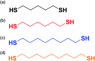 | ||
| Fig. 1 Chemical structures of the solvent additives used (a) 1,5-pentanedithiol (PDT), (b) 1,6-hexanedithiol (HDT), (c) 1,8-octanedithiol (ODT) and (d) 1,9-nonanedithiol (NDT). | ||
| Solvent Additive | Boiling Point/°C at 760 Torr | Vapor Pressure/Pa at 25 °C | |
|---|---|---|---|
| 1,5-pentanedithiol | PDT | 216 | 14.27 |
| 1,6-hexanedithiol | HDT | 242 | 6.85 |
| 1,8-octanedithiol | ODT | 270 | 1.60 |
| 1,9-nananedithiol | NDT | 284 | 0.91 |
Fig. 2 shows the J-V characteristics of the additive-added blends under AM 1.5G irradiation at 100 mW cm−2 and the summary of the device performance is tabulated in Table 2. The statistical variation in the device performance with the different alkanedithiols is shown in Fig. 2(b). The data presented in Fig. 2(b) are collected from 320 devices. Both pristine (NA) and thermally-annealed (TA) devices are also included for comparison. The pristine device shows the lowest PCE (<0.5%) due to its low short circuit current (JSC) and fill factor (FF). Heat treatment at elevated temperature (above the glass transition (Tg) of the polymer) was reported to induce reorganization of both polymer and fullerene phase which leads to improved nanomorphology.14 Therefore, the PCE improves 7-fold to 3.5% in the thermally-annealed device which is a result of both an increase in JSC and FF. In general, the additive incorporation improves the device performance as compared to the NA blend. However, these additive-blended devices exhibit huge variation in PCE ranging from 1 to 3% depending on the alkanedithiol chosen as shown in Fig. 2(b).
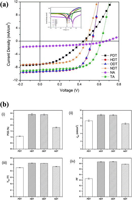 | ||
| Fig. 2 (a) Current density–voltage (J-V) characteristics of P3HT:PC61BM blend films under 100 mW cm−2 AM 1.5G illumination. Inset shows the same J-V characteristics in a logarithmic scale. (b) Statistical distribution of the device performance based on the different blends: (i) PCE, (ii) JSC, (iii) Voc and (iv) FF. | ||
| Conditions | J sc/mA cm−2 | V oc/V | FF | R s (Ω cm2) | R sh (Ω cm2) | PCE (%) |
|---|---|---|---|---|---|---|
| NA | 1.58 | 0.67 | 0.43 | 62.5 | 1127 | 0.46 |
| TA | 8.79 | 0.62 | 0.64 | 3.1 | 475 | 3.49 |
| PDT | 7.14 | 0.44 | 0.37 | 18 | 196 | 1.18 |
| HDT | 9.38 | 0.53 | 0.64 | 2.3 | 627 | 3.16 |
| ODT | 9.28 | 0.52 | 0.64 | 2.6 | 652 | 3.12 |
| NDT | 6.70 | 0.46 | 0.59 | 4.5 | 866 | 1.91 |
From Fig. 2(b), it can be observed that PCE increases as the alkyl chain length increases, with the exception of the NDT device. This trend is expected because as the Tb of additive increases, it takes a longer time for them to evaporate and therefore allows more time for phase separation. The best device is obtained from HDT with JSC of 9.38 mA cm−2, Voc of 0.53 V, FF of 0.64 V and PCE of 3.16%. The high PCE is comparable to that of the annealed device. The significantly enhanced PCE stems from the improvement in Jsc. The relatively high FF of the devices also indicates a low internal resistance in the blend. The trend in Jsc and FF of the devices can be correlated to the series resistance (Rs) of the devices listed in Table 2. The low Voc in additive processed devices is attributed to the upward shift in the HOMO level of P3HT as a result of its aggregation, which has also been observed in both thermally and solvent annealed devices.4,7 On the contrary, when the higher boiling point additive NDT was added into the blend, reductions in Jsc (by 30% as compared to the HDT-added device), Voc, FF and PCE were observed. The increase in Rs also suggests unoptimized blend morphology in the NDT processed blend film. The Vocreduction in the NDT-added device might also be attributed to the aggregation of PC61BM due to its poor interaction with NDT in the blend film which would induce a lower Voc in the OPV devices.33
Solubility of the components
The different extents of PC61BM aggregation can be correlated to the degree of intermolecular interactions between the additive molecules and the active materials, which are in turn dependent on the solubility parameter (δ) and the boiling point (Tb) of the solvents. The solubility parameter, which is often used to estimate the miscibility between organic solvents, is used to estimate the interaction strength. However, the duration of interaction is directly related to the boiling point of the additive. In this discussion, we determine the interaction parameters between the alkanedithiol and fullerene molecules. The interactions between the additive molecules and the host solvent are not considered based on the assumption that the host solvent molecules have evaporated during the initial stage of spin-coating. By using the group theory based on Small, Hoy and van Krevelen's approach,34 the solubility parameters were calculated for PDT, HDT, ODT and NDT giving values of 19.7, 19.2, 18.6 and 18.36 J1/2 cm−3/2 respectively. The δ for PC61BM using the same approach yields a value of 7.8 J1/2 cm−3/2. Two molecules are considered to have good interactions if the solubility parameter difference Δδ between the two molecules is as small as possible.Fig. 3 shows the correlation between the device PCE, the difference in solubility parameter and the boiling point of the additives. It can be observed that the optimum PCE is achieved at an optimal combination of both Tb and solubility parameter. Solvent additives with longer alkyl group and higher Tb favor the interaction with PC61BM molecules, as suggested from the smaller Δδ. Although the difference in solubility parameter between NDT and PC61BM is the smallest (ΔδNDT–PCBM = 10.56), its high Tb causes NDT to stay longer in the blend film during spin-coating. This provides sufficient time for NDT to interact with and then aggregate the fullerene molecules. Conversely, PDT with the lowest Tb gives the largest difference in solubility parameter with PC61BM (ΔδPDT–PCBM = 11.9) suggesting that the poor interaction between the two molecules may enhance the aggregation of PC61BM. The PDT device characteristics as shown in Table 2 are indeed lower than both HDT and ODT devices. The above observations imply that the extent of interaction between the additive and fullerenes depends on the strength and the duration of the interaction. The enhanced interaction can be obtained by choosing a solvent additive with as large a Δδ with either D or A as possible and by selecting an additive with high Tb. By modulating the choice of both δ and Tb of the additive, it is possible to adjust the extent of phase separation when the additive molecules are incorporated into the blend. In our study, the optimized blend morphology is obtained when either HDT or ODT is used which provides moderate degree of interaction with the fullerene molecules.
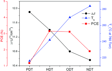 | ||
| Fig. 3 Relationship between boiling point, difference in solubility parameter and device PCE of the different additive systems. | ||
Absorption spectroscopy and grazing incidence X-ray diffraction
Both UV-vis absorption and X-ray diffraction measurements can give an insight to the aggregation and degree of order of the polymer chains. Fig. 4 depicts the UV-vis absorption spectra of the blend films added with the different additives. The inset in Fig. 4 compares the absorption behaviors of the additive-treated blend (PDT) with the untreated blends (pristine (NA) and thermally annealed (TA) blends). From the inset, we could observe that both the absorption profiles of TA and PDT blends have higher intensity and are more red-shifted than the NA blend. PDT blend even possesses a higher intensity than that of the TA blend, although the position of the main absorption peak at ca. 520 nm, which corresponds to a π–π* transition, and the two vibronic “shoulders” at ca. 550 nm and ca. 620 nm, which indicate the inter-chain interaction are very similar. The red-shift in absorption and the more prominent “shoulder” peaks are often correlated to a more extensive P3HT crystallinity in the blend. This indicates that PDT addition to the blend indeed has increased the amount of ordered regions in the blend. On the other hand, there is no significant variation observed from the absorption profiles of the different alkanedithiol blends in the main figure. Nevertheless, comparison across the different additive-added blends shows that PDT has slightly stronger absorption characteristics. The fact that PDT has the most intense absorption is a direct and strong indication that PDT induces P3HT interchain organization. Further proof of this enhanced crystallinity will be provided in the following XRD study.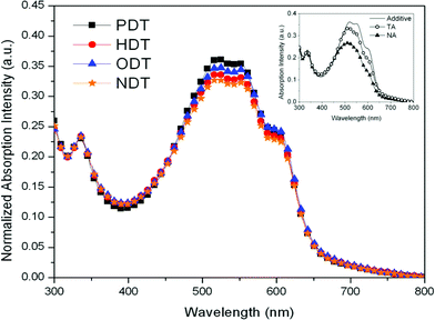 | ||
| Fig. 4 Absorption spectra of P3HT:PC61BM blends with different processing additives. The profiles are normalized at PCBM peak at ca. 330 nm. The inset focuses on the comparison between additive-treated and nontreated blends. | ||
To further quantify the extent of the P3HT crystallization in the different blends, a grazing incidence X-ray diffraction study was carried out on the different films. Fig. 5 shows the X-ray diffractograms of the different P3HT:PC61BM blends. The relative degree of P3HT crystallinity and the domain sizes of the different blend films are obtained by fitting the diffraction patterns of the (100) peaks at 2θ = 5.2° followed by the extraction of the diffraction intensity and the full width half maximum (FWHM). The reflection at (100) corresponds to the spacing between P3HT lamellae.35Fig. 5 shows that all blends processed with solvent additives possess a higher degree of crystallinity than the ones without the additive. Comparison of the area under the curve of the (100) peaks reveals that the P3HT phase in the PDT blend is the most crystalline, at least 25% more than the other blends. The relative FWHM as calculated from the peaks are 0.77, 0.88, 0.90 and 0.91 for PDT, HDT, ODT and NDT blends respectively. By using the Debye–Scherrer relationship, it can be estimated that the P3HT domain size in the PDT processed blend is the largest. The higher degree of crystallinity and the increase in the domain size of P3HT in the PDT blend is not attributed to Tb variation since the low Tb of PDT implies less opportunity for PDT to interact with P3HT after host solvent evaporation. Instead, the increase in domain size should be attributed to the poorer interaction between PDT and P3HT molecules. In addition, the large P3HT domain size also implies that severe P3HT and PC61BM segregation is present in the PDT blend. Finally, this GIXRD data indicates that the increase in both P3HT and PC61BM phase segregation reduces the donor–acceptor interfacial area, which causes a reduction in the exciton dissociation efficiency and hence lowers the device PCE (Fig. 2).
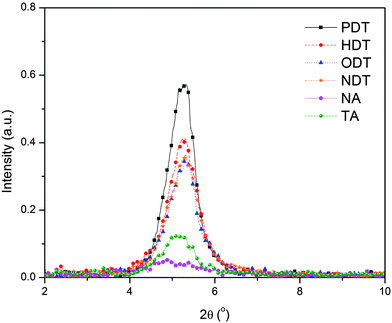 | ||
| Fig. 5 X-Ray diffraction results focusing on the (100) peak which corresponds to the P3HT phase in P3HT:PC61BM bulk heterojunction processed with different additives. | ||
Incident photon-to-current measurement and light intensity-dependent studies
The incident photon-to-current (IPCE) measurements were performed and the spectra for all the devices are shown in Fig. 6. The IPCE results are consistent with the optical absorption of the different P3HT:PC61BM blend films. The spectra of both annealed (TA) and additive-processed blends are more red-shifted than the pristine blend (NA) with the maximum IPCE around 55–65% in the wavelength range of 500–550 nm. Even though IPCE has often been correlated to the trend in Jsc and hence PCE20,22 the Jsc and IPCE trends in this work are not correlated. Fig. 2(b) shows that the Jsc of NDT is lower than that of HDT and ODT, while PDT results in the lowest Jsc. In Fig. 6, the NDT device has a comparable spectrum to those of HDT and ODT, while PDT addition results in the highest IPCE spectrum in spite of its lowest Jsc. The variation from the two measurements is believed to be due to the difference in light intensity used for illumination. Low-intensity monochromatic light illumination, which is significantly lower than the standard 1 sun PCE measurement, was used for IPCE measurement. Photovoltaic behaviors of PV devices may vary under different light intensities due to the change in recombination losses, charge-density dependent mobilities and space-charge effects.36–39 With respect to the quantum efficiency (QE) characteristics, Szmytowski has theoretically derived a set of relationships which show QE decreases as a function of light intensity and further showed that bimolecular recombination increases with increased light intensity.39 Consequently, the deviation in the PCE–IPCE relationships for PDT and NDT devices is suggested to be attributed to reduced bimolecular recombination at low light intensity.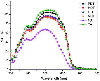 | ||
| Fig. 6 Incident photon-to-current efficiency (IPCE) spectra of the P3HT:PC61BM blend with different processing conditions. Organic photovoltaic devices are exposed to monochromatic light guided with optical cable. | ||
To investigate the loss of photocurrent in the alkanedithiol-added PV devices, the light intensity-dependent study was performed. Fig. 7 shows a double logarithmic diagram of the intensity dependence of Jsc of the devices, as well as the recombination parameters α derived from the power law J ∼ Pα.40 The α values can be correlated to the trend in PCE and this shows that the device performance is influenced by recombination process, whether it is geminate (α = 1) or bimolecular recombination (α = 0.5). The current densities of both HDT and ODT devices possess a close-to-linear dependence on the light intensity, implying the free charges are mainly lost due to geminate recombination. On the other hand, both NDT and PDT devices have lower α indicating an increased contribution of bimolecular recombination. This loss may be correlated to the change in blend morphology where finer phase separation will have less bimolecular recombination loss.38 So far, the deviation between the IPCE and PCE behaviors is explained in terms of the contribution of the bimolecular recombination. In the next sections, we shall look at how the different additives result in morphology variation.
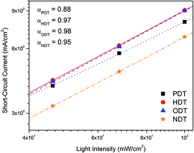 | ||
| Fig. 7 Light intensity dependence of short-circuit current for P3HT:PC61BM devices processed with different additives. The recombination parameters derived from power law by fitting the double-logarithmic relationships are also shown. | ||
Morphology characterization
From previous discussions, we suggested that the low device performance was caused by the unoptimized blend morphology with aggregation of P3HT and/or PC61BM molecules into domains with a non-ideal size for exciton dissociation and transport. To show conclusively that the unoptimized morphology is the reason for the variation in the device behaviors, we investigated the samples using AFM and STXM. AFM operated in the tapping mode was used to verify the extent of phase separation in the blends. Fig. 8 shows the 4 × 4 μm topographical and phase images of the different P3HT:PC61BM blends. The pristine (NA) blend appears to be smooth and featureless with a root-mean-square roughness (σRMS) of 0.9 nm. Thermal treatment of the same blend resulted in a slight increase in the surface roughness (σRMS = 1.4 nm), interconnected fibrillar features are also observed in this blend. The addition of high boiling point solvents such as alkanedithiols tends to enhance the aggregation of the polymer blends resulting in rougher surfaces.18,19 From the AFM study, it is difficult to resolve any significant difference among the additive-added blend films although their features are distinctly different from the non-additive counterparts. Regardless of the additive molecules used, these blends feature irregular domains ranging from 0.1–1 μm in size and the surface roughness of the blends is found to vary from 10–14 nm. In short, although AFM has been often used to resolve the difference between pristine and additive-treated samples, it may not be the most effective method to distinguish the nanomorphology and the phase segregation of the blend films treated with alkanedithiols. On top of this, it was reported that the P3HT-rich phase tends to segregate vertically on top of the PCBM-rich phase in additive-treated blends.18 Hence AFM, which is a surface technique, does not have the capability to provide sufficient information about the phase segregation in the blend films with additives.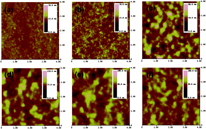 | ||
| Fig. 8 4 × 4 μm scans of tapping mode atomic force microscopy (AFM) height images of the P3HT:PCBM blend processed with different treatments: (a) as-cast (NA); (b) thermal annealing (TA); (c) PDT; (d) HDT; (e) ODT; and (f) NDT. | ||
STXM is a powerful synchrotron-based technique capable of resolving morphology49 and blend composition with nanoscale resolution, and it has been recently applied to investigate the effect of nanomorphology on photovoltaic device characteristics.41–45STXM can provide information on the bulk morphology and is therefore a good complementary technique to AFM in investigating the phase separation in polymer-fullerene blend. In this discussion we will show that this may be related to the increased PC61BM phase aggregation in the blend film upon NDT addition. The degree of phase separation of fullerene component is believed to be unfavorable for a balanced hole-electron transport that results in the low FF in the NDT system. In short, the choice of additive will affect the device performance which can be correlated to the change in blend morphology. Fig. 9 shows the 15 × 15 μm STXM images of the HDT and NDT blends obtained at both E ca. 200 eV and E ca. 285 eV, which are sensitive of sulfur and carbon X-ray absorption edges, respectively. For an image taken at E ca. 200 eV, the darker region corresponds to the sulfur-rich region; while for the image taken at E ca. 285 eV, the darker region corresponds to a carbon-rich region. Due to the varying contrast, we can qualitatively observe the P3HT (sulfur-rich) and PC61BM (carbon-rich) distribution in the sample. It is clear that the contrast difference between the domains/matrix area of the images taken at E ca. 285 eV is more obvious than the contrast difference of those taken at E ca. 200 eV. This implies that the phase segregation of PC61BM is more distinct and the domains are PC61BM-rich. On the other hand, the P3HT distribution in the domains and matrix regions is more uniform as can be seen from the low contrast differences of these two regions. It should also be noted that no further thickness and chemical mappings were done in this study. As revealed from the STXM measurement, P3HT:PC61BM blend processed with NDT tends to have larger “PC61BM-rich” domains (around 2–3 μm) distributed throughout the bulk whereas similar domains are smaller (around 0.5–1 μm in diameter) in the HDT-processed blend. The size difference of these micro-domains plays an important role in the device performance of the blend. The blend with HDT has smaller “PC61BM-rich” domains and does not suffer any loss in photocurrent suggesting that exciton dissociation and charge transport are equally optimized. This observation agrees with previous studies which found that smaller domains reduce the recombination probability and favors efficient exciton dissociation.46,47 In the NDT-processed blend, the larger PC61BM phase separation would promote efficient electron transport but compromise the amount of free charges generated due to the smaller D/A interfacial area. The lower PCE with low Jsc in the NDT system suggests exciton dissociation as the limiting factor rather than charge transport. The poorer performance in the PDT system may be contributed to by a similar factor, i.e. a significantly aggregated PC61BM phase in addition to the more severe P3HT aggregation as revealed from the GIXRD study.
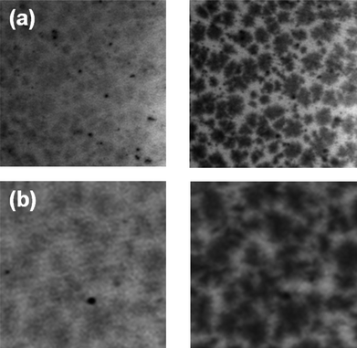 | ||
| Fig. 9 15 × 15 μm scanning transmission X-ray microscopy (STXM) images for P3HT:PC61BM blends processed with: (a) HDT and (b) NDT. The left images are taken at 200 eV and the right images are taken at 285 eV. | ||
In this study we have shown that the selection of the solvent additive is an important factor to obtain the ideal nanomorphology in a thermal-free OPV device. By choosing additive with proper solubility parameter and boiling point, such as HDT and ODT, it may be able to generate optimal phase separation, crucial in improving device performance.
Conclusions
We have systematically investigated the effect of alkanedithiols with different alkyl chain lengths on the photovoltaic behavior of the P3HT:PC61BM BHJ. In our attempt to refine the selection rules of these additive molecules, we found that both the boiling point (Tb) and solubility parameter (δ) of the additives are important parameters which should not be considered independently. Solvent additives with different Tb and δ can be used to modify the degree of intermolecular interaction in order to achieve phase segregation with the ideal domain size for optimal exciton dissociation and minimized bimolecular recombination. More PC61BM aggregation was observed either when PDT was used, due to the poor intermolecular interaction (i.e. high Δδ), or when NDT was used, because of its sufficiently long interaction duration with the active materials due to its high Tb. The blend morphologies with extensive phase separation such as in the PDT and NDT-added blends are unfavorable for exciton dissociation and charge transport. Nonetheless, optimization of blend morphology as in the HDT and ODT systems can lead to the improvement of device PCE to 3.1%. The understanding of the intermolecular interactions between the additive molecules and the blend active components opens up the possibility of a selection of appropriate solvent additive as morphological control agents. This is important for novel semiconducting materials whose morphologies cannot be controlled through conventional annealing treatments.Acknowledgements
This work is supported by the Science and Engineering Research Council, Agency for Science, Technology and Research (A*STAR), Singapore. Björn Bräuer would like to thank the German Research Foundation (DFG) for a postdoctoral fellowship. We thank Tolek Tyliszczak from the Advanced Light Source (ALS) in Berkeley for his help and the US Department of Energy for the financial support of ALS projects.References
- B. C. Thompson and J. M. J. Fréchet, Angew. Chem., Int. Ed., 2008, 47, 58 CrossRef.
- G. Dennler, M. C. Scharber and C. J. Brabec, Adv. Mater., 2009, 21, 1323 CrossRef CAS.
- L.-M. Chen, Z. Hong, G. Li and Y. Yang, Adv. Mater., 2009, 21, 1434 CrossRef CAS.
- W. Ma, C. Yang, X. Gong, K. Lee and A. J. Heeger, Adv. Funct. Mater., 2005, 15, 1617 CrossRef CAS.
- S. Günes, H. Neugebauer and N. S. Sariciftci, Chem. Rev., 2007, 107, 1324 CrossRef.
- J. Peet, J. Y. Kim, N. E. Coates, W. L. Ma, D. Moses, A. J. Heeger and G. C. Bazan, Nat. Mater., 2007, 6, 497 CrossRef CAS.
- G. Li, V. Shrotriya, J. Huang, Y. Yao, T. Moriarty, K. Emery and Y. Yang, Nat. Mater., 2005, 4, 864 CAS.
- H. Hoppe and N. S. Sariciftci, J. Mater. Chem., 2006, 16, 45 RSC.
- A. J. Moulé and K. Meerholz, Adv. Mater., 2008, 20, 240 CrossRef.
- A. J. Moulé and K. Meerholz, Adv. Funct. Mater., 2009, 19, 3028 CrossRef CAS.
- X. Yang, J. Loos, S. C. Veenstra, W. J. H. Verhees, M. M. Wienk, J. M. Kroon, M. A. J. Michels and R. A. J. Janssen, Nano Lett., 2005, 5, 579 CrossRef CAS.
- D. E. Markov, E. Amsterdam, P. W. M. Blom, A. B. Sieval and J. C. Hummelen, J. Phys. Chem. A, 2005, 109, 5266 CrossRef CAS.
- F. Padinger, R. S. Rittberger and N. S. Sariciftci, Adv. Funct. Mater., 2003, 13, 85 CrossRef CAS.
- J. Jo, S.-S. Kim, S.-I. Na, B.-K. Yu and D.-Y. Kim, Adv. Funct. Mater., 2009, 19, 866 CrossRef CAS.
- J. Ouyang and Y. Xia, Sol. Energy Mater. Sol. Cells, 2009, 93, 1592 CrossRef CAS.
- J. K. Lee, W. L. Ma, C. J. Brabec, J. Yuen, J. S. Moon, J. Y. Kim, K. Lee, G. C. Bazan and A. J. Heeger, J. Am. Chem. Soc., 2008, 130, 3619 CrossRef CAS.
- J. Peet, E. Brocker, Y. Xu and G. C. Bazan, Adv. Mater., 2008, 20, 1882 CrossRef CAS.
- Y. Yao, J. Hou, Z. Xu, G. Li and Y. Yang, Adv. Funct. Mater., 2008, 18, 1783 CrossRef CAS.
- A. Pivrikas, P. Stadler, H. Neugebauer and N. S. Sariciftci, Org. Electron., 2008, 9, 775 CrossRef CAS.
- H.-Y. Chen, H. Yang, G. Yang, S. Sista, R. Zadoyan, G. Li and Y. Yang, J. Phys. Chem. C, 2009, 113, 7946 CrossRef CAS.
- J. Peet, A. J. Heeger and G. C. Bazan, Acc. Chem. Res., 2009, 42, 1700 CrossRef CAS.
- Y.-M. Chang and L. Wang, J. Phys. Chem. C, 2008, 112, 17716 CrossRef CAS.
- J. K. Lee, N. E. Coates, S. Cho, N. S. Cho, D. Moses, G. C. Bazan, K. Lee and A. J. Heeger, Appl. Phys. Lett., 2008, 92, 243308 CrossRef.
- Y. Liang, Z. Xu, J. Xia, S.-T. Tsai, Y. Wu, G. Li, C. Ray and L. Yu, Adv. Mater., 2010, 22, E135 CrossRef CAS.
- R. Qin, W. Li, C. Li, C. Du, C. Veit, H.-F. Schleiermacher, M. Andersson, Z. Bo, Z. Liu, O. Inganäs, U. Wuerfel and F. Zhang, J. Am. Chem. Soc., 2009, 131, 14612 CrossRef CAS.
- S. Cho, J. K. Lee, J. S. Moon, J. Yuen, K. Lee and A. J. Heeger, Org. Electron., 2008, 9, 1107 CrossRef CAS.
- N. E. Coates, I.-W. Hwang, J. Peet, G. C. Bazan, D. Moses and A. J. Heeger, Appl. Phys. Lett., 2008, 93, 072105 CrossRef.
- M. Dante, A. Garcia and T.-Q. Nguyen, J. Phys. Chem. C, 2009, 113, 1596 CrossRef CAS.
- J. Peet, N. S. Cho, S. K. Lee and G. C. Bazan, Macromolecules, 2008, 41, 8655 CrossRef CAS.
- M. Morana, M. Wegscheider, A. Bonanni, N. Kopidakis, S. Shaheen, M. Scharber, Z. Zhu, D. Waller, R. Gaudiana and C. Brabec, Adv. Funct. Mater., 2008, 18, 1757 CrossRef CAS.
- C. V. Hoven, X.-D. Dang, R. C. Coffin, J. Peet, T.-Q. Nguyen and G. C. Bazan, Adv. Mater., 2010, 22, E63 CrossRef CAS.
- J. Peet, C. Soci, R. C. Coffin, T. Q. Nguyen, A. Mikhailovsky, D. Moses and G. C. Bazan, Appl. Phys. Lett., 2006, 89, 252105 CrossRef.
- P. A. Troshin, H. Hoppe, J. Renz, M. Egginger, J. Y. Mayorova, A. E. Goryachev, A. S. Peregudov, R. N. lyubovskaya, G. Gobsch, N. S. Sariciftci and V. F. Razumov, Adv. Funct. Mater., 2009, 19, 779 CrossRef CAS.
- D. W. van Krevelen, Properties of Polymers: Their Correlation with Chemical Structure; Their Numerical Estimation and Prediction from Additive Group Contributions, Elsevier Science Publishers, Amsterdam, London, New York, 1990 Search PubMed.
- H. Sirringhaus, P. J. Brown, R. H. Friend, M. M. Nielsen, K. Bechgaard, B. M. W. Langeveld-Voss, A. J. H. Spiering, R. A. J. Janssen, E. W. Meijer, P. Herwig and D. M. de Leeuw, Nature, 1999, 401, 685 CrossRef CAS.
- R. A. Marsh, C. R. McNeill, A. Abrusci, A. R. Campbell and R. H. Friend, Nano Lett., 2008, 8, 1393 CrossRef CAS.
- A. J. Moulé and K. Meerholz, Appl. Phys. B: Lasers Opt., 2008, 92, 209 CrossRef CAS.
- K. Maturovać, S. S. van Bavel, M. M. Wienk, R. A. J. Janssen and M. Kemerink, Nano Lett., 2009, 9, 3032 CrossRef CAS.
- J. Szmytkowski, J. Phys. D: Appl. Phys., 2007, 40, 3352 CrossRef CAS.
- M. Pope and C. E. Swenberg, Electronic Processes in Organic Crystals and Polymers, Oxford University Press Oxford, 1999 Search PubMed.
- C. R. McNeill, B. Watts, L. Thomsen, H. Ade, N. C. Greenham and P. C. Dastoor, Macromolecules, 2007, 40, 3263 CrossRef CAS.
- Christopher R. McNeill, B. Watts, L. Thomsen, Warwick J. Belcher, A. L. D. Kilcoyne, Neil C. Greenham and Paul C. Dastoor, Small, 2006, 2, 1432 CrossRef CAS.
- K. B. Burke, W. J. Belcher, L. Thomsen, B. Watts, C. R. McNeill, H. Ade and P. C. Dastoor, Macromolecules, 2009, 42, 3098 CrossRef CAS.
- C. R. McNeill, B. Watts, S. Swaraj, H. Ade, L. Thomsen, W. Belcher and P. C. Dastoor, Nanotechnology, 2008, 19, 424015 CrossRef.
- B. Watts, W. J. Belcher, L. Thomsen, H. Ade and P. C. Dastoor, Macromolecules, 2009, 42, 8392 CrossRef CAS.
- D. Veldman, O.z. İpek, S. C. J. Meskers, J.r. Sweelssen, M. M. Koetse, S. C. Veenstra, J. M. Kroon, S. S.v. Bavel, J. Loos and R. A. J. Janssen, J. Am. Chem. Soc., 2008, 130, 7721 CrossRef CAS.
- P. E. Keivanidis, T. M. Clarke, S. Lilliu, T. Agostinelli, J. E. Macdonald, J. R. Durrant, D. D. C. Bradley and J. Nelson, J. Phys. Chem. Lett., 2010, 1, 734 Search PubMed.
- A. L. D. Kilcoyne, T. Tyliszczak, W. F. Steele, S. Fakra, P. Hitchcock, K. Franck, E. Anderson, B. Harteneck, E. G. Rightor, G. E. Mitchell, A. P. Hitchcock, L. Yang, T. Warwick and H. J. Ade, J. Synchrotron Radiat., 2003, 10, 125 CrossRef CAS.
- B. Bräuer, A. Virkar, S. Mannsfeld, D. Bernstein, R. Kukreja, K. Chou, T. Tyliszczak, Z. Bao and Y. Acremann, Chem. Mater., 2010, 22, 3693 CrossRef CAS.
| This journal is © The Royal Society of Chemistry 2011 |